Communication

Rapid and Efficient NO2 Sensing Performance of TeO2 Nanowires

1
College of Automation & College of Artificial Intelligence, Nanjing University of Posts and Telecommunications, Nanjing 210023, China
2
School of Integrated Circuit Science and Engineering, Nanjing University of Posts and Telecommunications, Nanjing 210023, China
3
School of Geography and Biological Information, Nanjing University of Posts and Telecommunications, Nanjing 210023, China
*
Author to whom correspondence should be addressed.
These authors contributed equally to this work.
Sensors 2023, 23(22), 9097; https://doi.org/10.3390/s23229097
Submission received: 27 September 2023 / Revised: 2 November 2023 / Accepted: 8 November 2023 / Published: 10 November 2023
(This article belongs to the Section Nanosensors)

Abstract

:
Gas sensors play a pivotal role in environmental monitoring, with NO2 sensors standing out due to their exceptional selectivity and sensitivity. Yet, a prevalent challenge remains: the prolonged recovery time of many sensors, often spanning hundreds of seconds, compromises efficiency and undermines the precision of continuous detection. This paper introduces an efficient NO2 sensor using TeO2 nanowires, offering significantly reduced recovery times. The TeO2 nanowires, prepared through a straightforward thermal oxidation process, exhibit a unique yet smooth surface. The structural characterizations confirm the formation of pure-phase TeO2 after the anneal oxidation. TeO2 nanowires are extremely sensitive to NO2 gas, and the maximum response (defined as the ratio of resistance in the air to that under the target gas) to NO2 (10 ppm) is 1.559. In addition, TeO2 nanowire-based sensors can return to the initial state in about 6–7 s at 100 °C. The high sensitivity can be attributed to the length–diameter rate, which adsorbs more NO2 to facilitate the electron transfer. The fast recovery is due to the smooth surface without pores on TeO2 nanowires, which may release NO2 quickly after stopping the gas supply. The present approach for sensing TeO2 nanowires can be extended to other sensor systems as an efficient, accurate, and low-priced tactic to enhance sensor performance.

1. Introduction

With the worsening of environmental pollution, poisonous gas emissions, the energy crisis, and other problems, the demand for better selectivity, lower power consumption, and higher sensitivity of gas sensors is becoming increasingly urgent. However, toxic gas, like NO2, which can lead to an array of health complications such as nausea, respiratory tract irritation, asthma, asphyxiation, and, in severe cases, death [1], is hazardous. The recovery time of most NO2 sensors is about tens of or hundreds of seconds long, resulting in low efficiency and less accuracy in detection. As a result, a gas sensor nanomaterial needs to be exploited, which possesses a shorter sensing time.
Previously, various materials have been applied for sensing NO2; for example, Choi obtained that ZnO has gas sensitivity to NO2 gas, high selectivity, reasonable stability, and highly responsive sensing properties even in water vapor molecules. However, even if the ZnO is placed in a high-temperature environment, the fastest recovery time of it is still about 500 to 1000 s. The sample in this report was a 2D material with multiple rough holes. We believe this structure-stranded molecules’ movement is not conducive to releasing NO2 and would somewhat slow the recovery speed. Moreover, the selectivity of the gas sensor was reported to be poor [2].
In recent years, gas sensors based on metal oxide semiconductors have been applied mainly to this area because of their excellent performance, high stability, and floor price [3]. Materials with larger surface areas and smaller grain sizes are a priority for achieving high-performance gas sensors [4,5,6]. Therefore, quasi-one-dimensional oxide semiconductor nanomaterials are ideal for gas-sensitive applications due to their large surface-volume ratio and size effects. Mature gas-sensitive materials, such as SnO2 [7,8], ZnO [9], WO3 [10,11], Ga2O3 [12], and In2O3 [13] quasi-one-dimensional nanostructures, compared with relevant thin-film materials, have higher sensitivity, quicker response times, and more significant capability to detect low-concentration gases. However, they also have the disadvantages of poor selectivity, high sensing temperatures [14], and prolonged recovery time.
Previous studies of gas-sensing materials were usually according to n-type semiconductors for sensing investigations [15,16]. Nevertheless, few people pay attention to p-type semiconductors, like tellurium dioxide (TeO2), as gas sensors [17]. TeO2 is a widely used wide-band-gap semiconductor material. Because of its excellent acousto-optic and electro-optic properties [18], active optical devices widely make use of single-crystal TeO2 materials such as deflectors [19], modulators [20], tunable filters [21], hydrogen production [22,23], and potential antifungal agents [24]. When exposed to reducing gases, the outer layer of tellurium dioxide in semiconductor oxides reacts. Electrons trapped by oxygen are relayed to the semiconductor, decreasing the gas sensor’s resistance. Wansik Oum uses carbon-decorated TeO2, which has a more apparent corresponding coefficient at room temperature. A-C-decorated TeO2 nanowires have good selectivity to NO2 gas. The C-layer on the surface of the nanowires facilitates the transfer of holes. Nevertheless, the recovery time at room temperature is as long as 300 to 500 s. TeO2 in the report had a smooth surface and was covered by amorphous carbon (a-C) materials. This approach, however, hinders the release of NO2 molecules, resulting in slower recovery [25].
We believe that nanomaterials with smooth and undulating surfaces can accelerate the release rate of NO2 while expanding the effective surface area. At the same time, a rough or too-smooth surface can absorb more NO2 but will hinder its release rate, and the long recovery time may seriously impede the sensing application of nanowires. In this paper, TeO2 nanowires are oxidized via the natural oxidization of Te nanowires, which show high selectivity and sensitivity to NO2, and ultrafast recovery speed. Sensors based on TeO2 nanowires can revert to their initial state in approximately 6 to 7 s. The proposed gas sensor’s unique advantages include simple manufacturing, floor price, excellent selectivity, and good recovery time, which can be used in actual applications for NO2 sensing.

2. Experimental Details

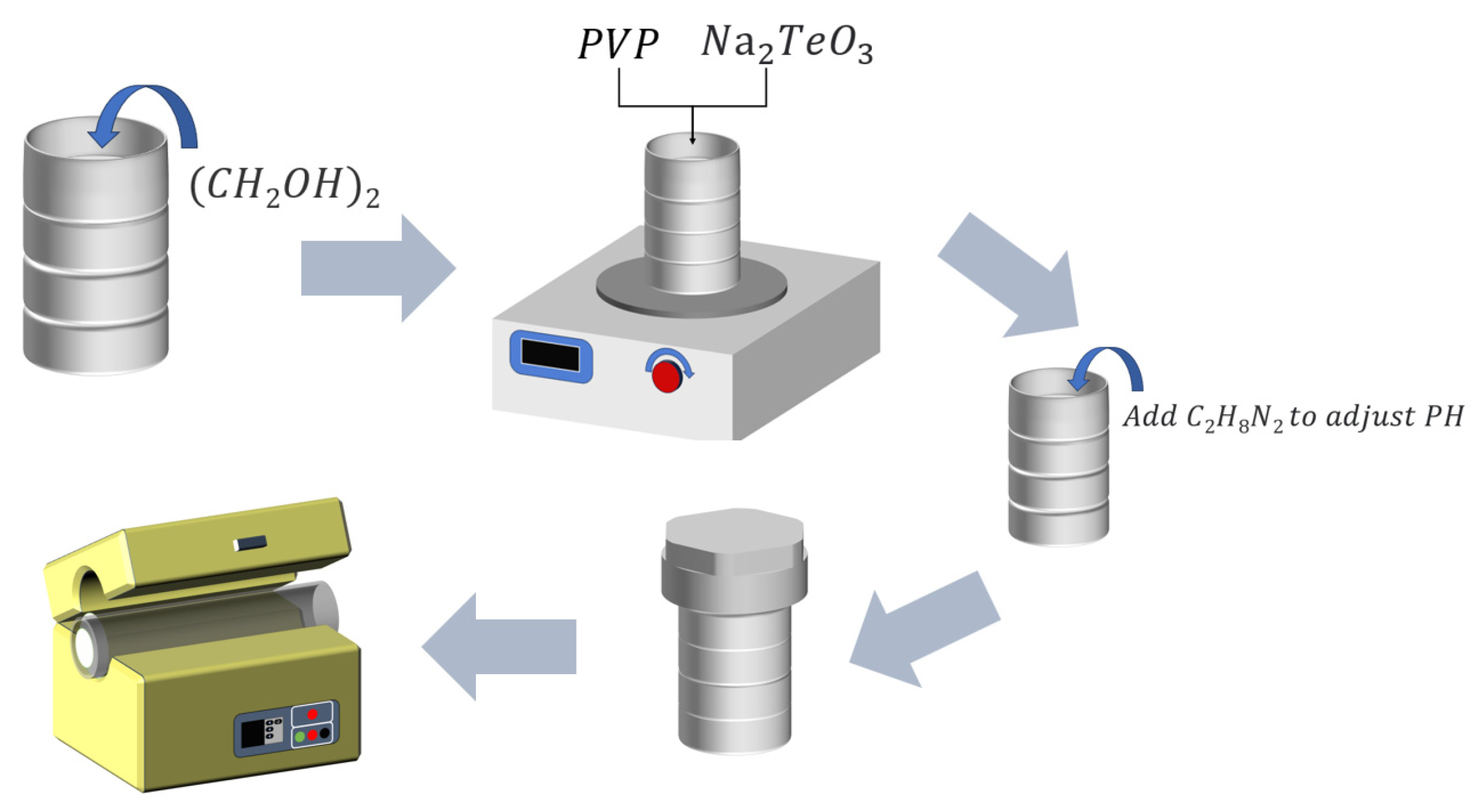
2.1. Sample Preparation

As shown in Figure 1, 25 mL of ethylene glycol solution was put into a polytetrafluoroethylene reaction kettle, followed by a 1.3 g polyvinylpyrrolidone (PVP) addition. The mixture was stirred with a magnetic stirring bar until it became transparent. Then, we added 1 mM of Na2TeO3 and stirred well for 2 h, followed by adding 1 mL of ethylenediamine solution to adjust the pH (the alkaline solution is convenient for replacing Te). The mixture was then placed in an oven at 180 °C for 3.5 h. After the reaction, it was repeatedly suction-filtered with water and ethanol. Then, it dried in a vacuum drying oven at 50 °C for 2 h to finally obtain a bulk product with a silvery-white and metallic luster. We put it into a 2 mL centrifuge tube, followed by adding 1 mL of ethanol, which was put in an ultrasonic machine for a short time and shaken several times to disperse the sample. Finally, it was dropped on a silicon wafer for observation.
To determine the best synthesis requirement for the oxidation of Te NWs to shape TeO2 nanowires, a series of heat treatments were performed at different temperature ranges (200 °C, 250 °C, 300 °C, and 350 °C) for a period of time. Ultimately, Te nanowires were annealed at the optimal temperature of 360 °C for 5.5 h and converted into high-quality nanowires using a high-temperature vacuum tube furnace [26].

2.2. Phase Analysis Method

The crystalline structure of the Te and TeO2 nanowires were characterized via X-ray diffraction (XRD, Bruker D8) using Cu Kα radiation (λ = 0.15406 nm) and further studied via high-resolution transmission electron microscopy (HRTEM JEOL-2100F, Tokyo, Japan). Observation of its morphology was conducted using field-emission-scanning electron microscopy (FE-SEM, JEOL JSM–7401F, Yangzhou, China). Raman spectra were obtained using a modified micro-Raman system (Invia Basic Renishaw, Nanjing, China) using an excitation laser wavelength of 514 nm, linking an Olympus microscope with a CCD detector and a Spex 1740 spectrometer. The transmission spectra were obtained using a UV-visible spectrophotometer (Thermo Scientific Evolution 201, Nanjing, China). A Thermo Scientific Nexsa XPS spectrometer with a monochromatic, micro-focused, low-power Al K-Alpha X-ray source selected photons with a 400 µm X-ray spot size and collected XPS spectra using a dual-focusing hemispherical analyzer with an energy of 50 eV.

2.3. Gas Analysis Method

The gas sensing experiments were conducted on an STP4 intelligent gas sensing analysis system (Nanjing Wisens Co., Ltd., China). To better estimate the performance of gas sensors, a method was adopted by measuring the resistance value of the gas sensors in a specified gas. The sensor’s resistance in the presence of air (Ra) and the target gas under a specified pressure (Rg) were measured, and the response was calculated using R = Ra/Rg. The recovery and response times calculation was based on the duration required to achieve a 90% resistance change when the target gas was introduced and halted separately.

3. Results and Discussion

3.1. Sample Characterization

Figure 2a,b shows Te’s SEM and HRTEM images and the successfully synthesized Te lines of sufficient length. The SEM images are shown in Figure 2a. The solvothermal synthesis products were linear and had good morphology. The externally synthesized Te nanowires do not have apparent roughness on the outer surface; the surface is smooth. The internal structure is uniform without noticeable defects. This indicates that the synthesized Te nanowires possess high-quality characteristics. Nanowires were about 10- to 40-μm-long and about 60 nm in diameter. Figure 2b indicates a high-resolution transmission electron microscopy (HRTEM) image of tellurium nanowires. The interplanar spacing of the tellurium nanowires was 0.59 nm, indicating tellurium growth in the [001] direction.
The XRD pattern of the solvothermal synthesis product is shown in Figure 2c. No impurity peaks were found at the diffraction peak, indicating that our daily standard product tellurium was successfully synthesized via this method.
The Raman spectrum for the tellurium is shown in Figure 2d, with three distinct peaks at 91, 120, and 141 cm−1. The 91 cm−1 mode was caused by chain expansion, while the 120 and 141 cm−1 modes indicated that bond bending and bond stretching was induced, which is consistent with the conclusions of related papers [26].
SEM and HRTEM images of the TeO2 are shown in Figure 3, indicating that a sufficiently long TeO2 image with a diameter of approximately 100–400 nm and a length of above 100–200 μm had been successfully synthesized. The shape was like a tree branch, the gas contact area was large, and the surface was not cracked.
Figure 3c shows the XRD pattern of the obtained product, indicating the formation of a high-quality tetragonal TeO2 crystal phase. All peaks are consistent with high-quality tetragonal TeO2 crystals, with lattice parameters (a = 4.796 A, c = 7.626 A, α = β = γ = 90°) which perfectly match the standard JCPDS data (JCPDS No.11-0693). The essence of highly crystalline TeO2 NWs is reflected in the appearance of sharp peaks. This means that the crystal is highly intact, with high purity and integrity, without significant defects or crystal distortions. This information is crucial for the study of the material’s crystal structure and quality.
Raman spectroscopy can be used to study the molecular vibrations and lattice vibrations of materials, providing information about material properties and phonon dynamics. The Raman spectra of pristine TeO2 nanowires, as shown in Figure 3d, indicated that the peak of 520 cm−1 was identified as the characteristic Raman peak of silicon, possibly originating from the Si substrate. The Raman distinct peak at 307 cm−1 matches the 2TA vibration mode of Si.
On the other side of the shield, the Raman peaks near 823 cm−1 and 229 cm−1 are related to the B1 vibration mode of TeO2, while the peaks near 427 cm−1 are related to the B2 mode. Additionally, the peak at 649 cm−1 is related to the A1 mode, and a relatively sharp peak was observed at 685 cm−1, corresponding to the E mode of TeO2 [27]. The sharp and distinct peaks observed in the Raman spectrum indicate that the TeO2 nanowires grown in the samples are of high quality.
The analysis conducted using X-ray photoelectron spectroscopy (XPS) confirmed that the obtained product is TeO2. The XPS survey of the TeO2 nanowires in Figure 4a displays two prominent peaks corresponding to the Te and O elements. In Figure 4b, the Te 3d region reveals peaks at 587.88 and 577.38 eV for Te 3d3/2 and Te 3d5/2, respectively, indicating the presence of TeO2 formation. Figure 4c displays the association of the peak at 530.6 eV in the O 1s binding energy region with TeO2. We conducted optical absorption spectroscopy tests to investigate the optical properties of the material. In Figure 4d, the optical absorption spectrum of the TeO2 nanowire samples is displayed within a wavelength range of 200–800 nm. Within this absorption spectrum, the maximum absorption peak is observed in the 200–400 nm wavelength range. This implies that TeO2 nanowire samples exhibit significant light absorption within this specific range of wavelengths. However, when the wavelength exceeds this range, the absorption intensity decreases sharply. This suggests that within the visible light and near-ultraviolet range, TeO2 nanowire samples exhibit pronounced light absorption, while the absorption significantly diminishes at longer wavelengths. This absorption spectrum characteristic is vital for understanding the material’s optical properties and potential applications.

3.2. Gas-Sensing Character

The resistance-based gas sensor uses the interactions between the gas and the resistance to detect the target gas. In this sensor, a resistors element is exposed to a gaseous environment. When the target gas is in contact with the resistive element, the target gas will chemically react or adsorb with the surface of the resistive element, resulting in a change in electrical resistance.
Figure 5 displays the curve of the TeO2 gas sensor. This figure shows the transient resistance of the TeO2 nanowires to NO2 gas at 300 °C. It was clear that the p-type properties of the synthesized TeO2 nanowires have been demonstrated through their resistance changes. In Figure 5a, the responses of the TeO2 gas sensor to 6, 10, and 14 ppm of NO2 gas were 1.302, 1.354, and 1.376, separately. These results indicate that the response of the TeO2 gas sensor is highly significant at a given gas concentration. In the presence of the gas, the TeO2 nanowire resistance changes due to the interaction between the nitrogen dioxide and the nanowires. This interaction may be adsorption of gas molecules or chemical reaction with the surface of the nanowire, resulting in altered resistance. The response value of the sensor can be used to determine the presence and concentration of the target gas. As the concentration of nitrogen dioxide gas increases, the response value of the sensor also increases. This indicates that the TeO2 gas sensor has good sensitivity to nitrogen dioxide gas and enables efficient detection at lower gas concentrations
To evaluate the behavior of the TeO2 gas sensor at different temperatures, we conducted an in-depth study of gas sensing at multiple temperatures. Figure 5b shows the transient response and resistance plot of the TeO2 nanowire sensor to NO2 gas at 50, 100, and 150 °C, separately. The sensor responses were 1.559, 1.348, and 1.159, respectively. Therefore, it is concluded that the optimal experimental temperature of TeO2 for NO2 is 50 °C and that the corresponding effect gradually weakened with the temperature increase. At lower temperature, TeO2 nanowires have better nitrogen 2 adsorption capacity and higher sensitivity. When the temperature increases, the interaction of the target gas with the sensor surface may be weakened, thus weakening the response. This may be due to the increased temperature leading to a more intense movement of the gas molecules, which reduces the adsorption capacity or reaction rate of the gas and the sensor surface.
Figure 5c reveals the response and resistance value of the TeO2 nanowire sensor to interference gas at a temperature of 50 °C. The sensor responds to NO2, CO, and acetone at a concentration of 10 ppm 1.376, 1.029, and 1.022, respectively. TeO2 showed outstanding selectivity for NO2. The sensor showed clear selectivity against NO, with the highest response values to NO gas, much higher than the response values for CO and acetone. This suggests that the TeO2 nanowire sensor has higher selectivity and lower interference response to nitrogen 2.
Through the curve in Figure 5d, it can also be seen that the response and the recovery times were very short, which were about 6 s long. Table 1 compares the recovery time in this work to other NO2 gas-sensing materials. Furthermore, as shown in Table 1, we can observe faster recovery times for TeO2 nanowire sensors compared to other semiconducting gas-sensing materials. This means that the sensor is able to recover to the base state from the target gas. This is important for continuous monitoring and real-time detection because a faster recovery time allows the sensor to be ready for the next measurement or detection.
To explore the repeatability of the sensors, we built two sensors using the same materials and manufacturing procedures. The response of the two sensors to NO2 gas was almost the same, irrespective of the concentration in the range of 2–10 ppm, demonstrating its excellent repeatability.

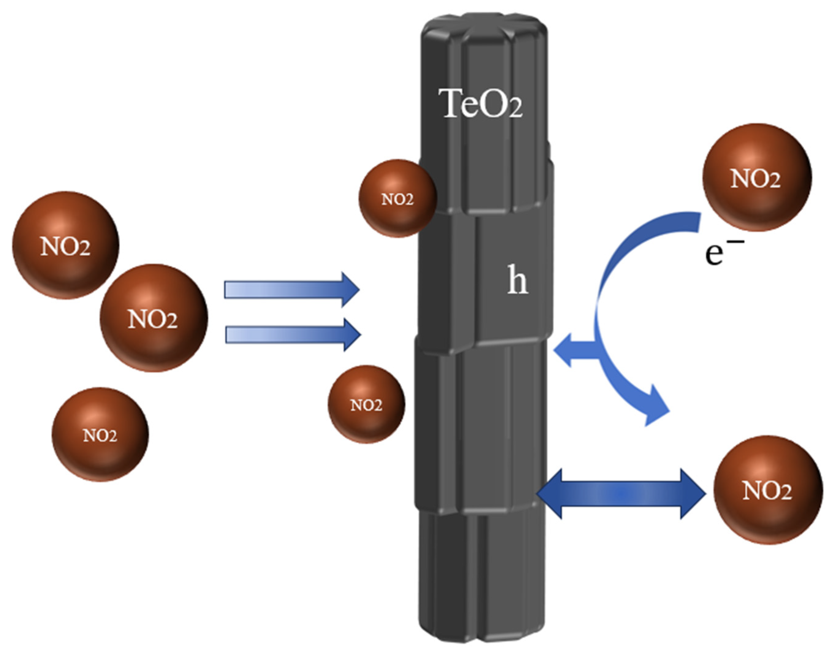
4. Mechanism Analysis

The definite sensing framework of the TeO2 materials for NO2 gas still needs further research. A widely accepted explanation for the gas-sensing mechanism of gas-sensitive oxide is that when semiconductor oxides are exposed to reducing gases, tellurium dioxide outside the semiconductor responds to the reducing gas. The electrons are caught by oxygen and transferred to the semiconductor, thereby reducing the resistance of the gas sensor. As to n-type semiconductors, the resistance is reduced because of the enhancement of the concentration of electrons in the semiconductor. P-type semiconductors’ resistance rises when holes combine with electrons released by surface reactions [33]. When exposed to oxidative gas, the gas species serve as an acceptor, leading to a rise in the resistance of the n-type semiconductor and a reduction in the resistance of the p-type semiconductor. In this study, the sensor’s resistance decreasing under NO2 reveals that TeO2 nanowires exhibit p-type conductivity [34].
Upon exposure to the oxidizing gas NO2, the NO2 molecule is adsorbed on the surface of TeO2 as an acceptor. The NO2 molecule, with an unpaired electron response with the suspension bond on top of TeO2, successfully catches a solitary pair of electrons in the suspension bond and forms a free hole. The mechanism of chemical interaction between NO2 molecules and TeO2 nanowires (Figure 6) can describe the equation [33]:
T e O 2 + N O 2 ( g ) T e O 2 N O 2 a d T e O 2 + N O 2 a d + h .
As a result, the hole concentration as the majority carrier in TeO2 nanowires rises, and the resistance diminishes. The sample presents a wrinkled morphology. The large surface area is the reason for the high sensitivity, as it potentially adsorbs more NO2, facilitating electron transfer. The quick recovery of the TeO2 nanowires results from their smooth, pore-less surface, which likely allows for the rapid release of NO2 once the gas supply is halted.
In conclusion, TeO2 nanowires have a tetragonal phase structure, are sensitive to NO2 gas, and have a typical p-type response. These results demonstrate the possibility of using TeO2 nanowires to manufacture low-power gas sensors.

5. Conclusions

In summary, TeO2 nanowire structures were prepared using a facile thermal oxidation method. The results showed that the TeO2 nanowires had a very fast reaction effect and recovery speed to NO2 gas. Their reaction time was about 10 s, while their recovery time was about 6 to 7 s at the temperature of 100 °C. At 50 °C, the response of TeO2 to NO2 reaches 1.559. The prepared TeO2 sensor realized low power consumption and high efficiency at a low temperature, showing applicability for safe and stable NO2 detection in the industrial field. The present work presents a valuable and potential design for developing NO2 gas sensors with excellent high-speed sensing performance.

Author Contributions

Conceptualization, S.Y.; Methodology, S.Y.; Writing—Original Draft Preparation, Y.S. and K.W.; Writing—Review and Editing, H.L., L.C. and Z.J.; Project Administration, S.Y. All authors have read and agreed to the published version of the manuscript.

Funding

This work is supported by the National Science Foundations of China (No. 62274093, No. 61991431), the Excellent Youth Foundation of Jiangsu Scientific Committee (BK20211538), and the National Basic Research Program of China (2018YFA0209100).

Data Availability Statement

Not available.

Conflicts of Interest

The authors declare no conflict of interest.

References

  1. Pan, Z.; Zhang, Y.; Cheng, Z.; Liang, B.; Zhang, J.; Li, X.; Wang, X.; Liu, D.; Yang, A.; Rong, M.; et al. A high-integration sensor array sensitive to oxynitride mixture. Sens. Actuators B Chem. 2017, 245, 183–188. [Google Scholar] [CrossRef]
  2. Choi, M.S.; Kim, M.Y.; Mirzaei, A.; Kim, H.S.; Kim, S.I.; Baek, S.H.; Chun, D.W.; Jin, C.H.; Lee, K.H. Selective, sensitive, and stable NO2 gas sensor based on porous ZnO nanosheets. Appl. Surf. Sci. 2021, 568, 150910. [Google Scholar] [CrossRef]
  3. Kim, J.H.; Kim, J.Y.; Lee, J.H.; Mirzaei, A.; Kim, H.W.; Hishita, S.; Kim, S.S. Indiumimplantation-induced enhancement of gas sensing behaviors of SnO2 nanowires by the formation of homo-core-shell structure. Sens. Actuators B Chem. 2020, 321, 128475. [Google Scholar] [CrossRef]
  4. Yamazoe, N. Toward innovations of gas sensor technology. Sens. Actuators B Chem. 2005, 108, 2–4. [Google Scholar] [CrossRef]
  5. Eranna, G.; Joshi, B.C.; Runthala, D.P.; Gupta, R.P. Oxide materials for development of integrated gas sensors—A comprehensive reviewCrit. Rev. Solid State Mater. Sci. 2004, 29, 111–188. [Google Scholar]
  6. Yamazoe, N. New approaches for improving semiconductor gas sensors. Sens. Actuators B Chem. 1991, 5, 7–9. [Google Scholar] [CrossRef]
  7. Comini, E.; Faglia, G.; Sberveglieri, G.; Pan, Z.W.; Wang, Z.L. Stable and highly sensitive gas sensors based on semiconducting oxide nanobelts. Appl. Phys. Lett. 2002, 81, 1869–1871. [Google Scholar] [CrossRef]
  8. Comini, E.; Faglia, G.; Sberveglieri, G.; Calestani, D.; Zanotti, L.; Zha, M. Tin oxide nanobelts electrical and sensing properties. Sens. Actuators B Chem. 2005, 111, 2–6. [Google Scholar] [CrossRef]
  9. Wan, Q.; Li, Q.H.; Chen, Y.J.; Wang, T.H.; He, X.L.; Li, J.P.; Lin, C.L. Fabrication and ethanol sensing characteristics of ZnO nanowire gas sensors. Appl. Phys. Lett. 2004, 84, 3654–3656. [Google Scholar] [CrossRef]
  10. Sawicka, K.M.; Prasad, A.K.; Gouma, P.I. Metal oxide nanowires for use in chemical sensing applications. Sens. Lett. 2005, 3, 31–35. [Google Scholar] [CrossRef]
  11. Ponzoni, A.; Comini, E.; Sberveglieri, G.; Zhou, J.; Deng, S.Z.; Xu, N.S.; Ding, Y.; Wang, Z.L. Ultrasensitive and highly selective gas sensors using three-dimensional tungsten oxide nanowire networks. Appl. Phys. Lett. 2006, 88, 203101. [Google Scholar] [CrossRef]
  12. Feng, P.; Xue, X.Y.; Liu, Y.G.; Wan, Q.; Wang, T.H. Achieving fast oxygen response in individual beta-Ga2O3 nanowires by ultraviolet illumination. Appl. Phys. Lett. 2006, 89, 112114. [Google Scholar] [CrossRef]
  13. Li, C.; Zhang, D.H.; Liu, X.L.; Han, S.; Tang, T.; Han, J.; Zhou, C.W. Chemical gating of In2O3 nanowires by organic and biomolecules. Appl. Phys. Lett. 2003, 83, 4014–4016. [Google Scholar] [CrossRef]
  14. Raut, B.T.; Godse, P.R.; Pawar, S.G.; Chougule, M.A.; Bandgar, D.K.; Patil, V.B. Novel method for fabrication of polyaniline-CdS sensor for H2S gas detection. Measurement 2012, 45, 94–100. [Google Scholar] [CrossRef]
  15. Sonker, R.K.; Sabhajeet, S.R.; Singh, S.; Yadav, B.C. Synthesis of ZnO nanopetals and its application as NO2 gas sensor. Mater. Lett. 2015, 152, 189–191. [Google Scholar] [CrossRef]
  16. Ma, H.; Yu, L.; Yuan, X.; Li, Y.; Li, C.; Yin, M.; Fan, X. Room temperature photoelectric NO2 gas sensor based on direct growth of walnut-like In2O3 nanostructures. J. Alloys Compd. 2019, 782, 1121–1126. [Google Scholar] [CrossRef]
  17. Jiang, Z.Y.; Xie, Z.X.; Zhang, X.H.; Xie, S.Y.; Huang, R.B.; Zheng, L.S. Inorg. Synthesis of silver nanotubes by electroless deposition in porous anodic aluminium oxide templates. Chem. Commun. 2004, 9, 1106–1107. [Google Scholar]
  18. Mebougna, L.D.; Stephen, U.E.; Ifechukwude, O.O.; Dominique, E.J.; Anwar, H.; Ralph, B.J. Analysis of Te and TeO2 on CdZnTe Nuclear Detectors Treated with Hydrogen Bromide and Ammonium-Based Solutions. J. Mater. Sci. Chem. Eng. 2017, 5, 9–18. [Google Scholar]
  19. Warner, A.W.; White, D.L.; Bonner, W.A. Acousto-optic light deflectors using optical activity in paratellurite. J. Appl. Phys. 1972, 43, 4489–4495. [Google Scholar] [CrossRef]
  20. Antonov, S.N. Acoustooptic nonpolar light controlling devices and polarization modulators based on paratellurite crystals. Tech. Phys. 2004, 49, 1329–1334. [Google Scholar] [CrossRef]
  21. Gupta, N.; Voloshinov, V. Hyperspectral imaging performance of a TeO2 acousto-optic tunable filter in the ultraviolet region. Opt. Lett. 2005, 30, 985–987. [Google Scholar] [CrossRef] [PubMed]
  22. Rao, V.N.; Sairam, P.K.; Kim, M.-D.; Rezakazemi, M.; Aminabhavi, T.M.; Ahn, C.W.; Yang, J.-M. CdS/TiO2 nano hybrid heterostructured materials for superior hydrogen production and gas sensor applications. J. Environ. Manag. 2023, 340, 117895. [Google Scholar]
  23. Rao, V.N.; Ravi, P.; Sathish, M.; Cheralathan, K.K.; Neppolian, B.; Kumari, M.M.; Shankar, M.V. Manifestation of enhanced and durable photocatalytic H2 production using hierarchically structured Pt@Co3O4/TiO2 ternary nanocomposite. Ceram. Int. 2021, 47, 10226–103235. [Google Scholar]
  24. El-Sayyad, G.S.; Mosallam, F.M.; El-Sayed, S.S.; El-Batal, A.I. Facile Biosynthesis of Tellurium Dioxide Nanoparticles by Streptomyces cyaneus Melanin Pigment and Gamma Radiation for Repressing Some Aspergillus Pathogens and Bacterial Wound Cultures. J. Clust. Sci. 2020, 31, 147–159. [Google Scholar] [CrossRef]
  25. Oum, W.; Mirzaei, A.; Hussain, T.; Bang, J.H.; Ha, S.; Shin, K.Y.; Yu, D.J.; Kang, S.; Kaewmaraya, T.; Kim, S.S.; et al. Room temperature NO2 sensing performance of a-C-decorated TeO2 nanowires. Sens. Actuators: B Chem. 2022, 363, 131853. [Google Scholar] [CrossRef]
  26. Zhu, H.L.; Chen, J.H.; Fan, L.; Liu, H.; Wei, Q.C.; Hu, M.D.; Kong, L.J.; Zhang, J.W.; Yan, S.C. Photoelectric properties of tellurium nanowires by a green thermal solvothermal method. Mater. Express 2022, 12, 511–517. [Google Scholar] [CrossRef]
  27. Kim, S.S.; Park, J.Y.; Choi, S.W.; Na, H.G.; Yang, J.C.; Kwak, D.S.; Nam, H.J.; Hwangbo, C.K.; Kim, H.W. Drastic change in shape of tetragonal TeO2 nanowires and their application to transparent chemical gas sensors. Appl. Surf. Sci. 2011, 258, 510–516. [Google Scholar] [CrossRef]
  28. Zhao, H.; Ge, W.Y.; Tian, Y.; Wang, P.T.; Li, X.; Liu, Z.F. Pr2Sn2O7/NiO heterojunction for ultra-fast and low operating temperature to NO2 gas sensing. Sens. Actuators A Phys. 2023, 349, 114100. [Google Scholar] [CrossRef]
  29. Behera, B.; Chandra, S. Synthesis of WO3 nanorods by thermal oxidation technique for NO2 gas sensing application. Mater. Sci. Semicond. Process. 2018, 86, 79–84. [Google Scholar] [CrossRef]
  30. D’Urso, L.; Compagnini, G.; Puglisi, O. sp/sp2 bonding ratio in sp rich amorphous carbon thin films. Carbon 2006, 44, 2093–2096. [Google Scholar] [CrossRef]
  31. Choi, M.S.; Na, H.G.; Bang, J.H.; Mirzaei, A.; Han, S.; Lee, H.Y.; Kim, S.S.; Kim, H.W.; Jin, C. SnO2 nanowires decorated by insulating amorphous carbon layers for improved room-temperature NO2 sensing. Sens. Actuators B Chem. 2021, 326, 128801. [Google Scholar] [CrossRef]
  32. Han, T.H.; Bak, S.Y.; Kim, S.; Lee, S.H.; Han, Y.J.; Yi, M. Decoration of CuO NWs Gas Sensor with ZnO NPs for Improving NO2 Sensing Characteristics. Sensors 2021, 21, 2103. [Google Scholar] [CrossRef] [PubMed]
  33. Liu, Z.F.; Yamazaki, T.; Shen, Y.; Kikuta, T.; Nakatani, N.; Kawabata, T. Room temperature gas sensing of p-type TeO2 nanowires. Appl. Phys. Lett. 2007, 90, 173119. [Google Scholar] [CrossRef]
  34. Shen, Y.B.; Wei, D.Z.; Ma, J.W.; Zhang, B.Q. Preparation and room-temperature NO2 sensing properties of TeO2 nanowires. J. Northeast. Univ. 2014, 35, 1019–1022. [Google Scholar]
Figure 1. Scheme of the sample preparation process.
Sensors 23 09097 g001
Figure 2. SEM and HRTEM analysis of Te nanowires. (a,b) XRD and Raman spectra of Te nanowires (c,d).
Sensors 23 09097 g002
Figure 3. SEM and HRTEM analysis of TeO2 nanowires. (a,b) XRD and Raman spectra of TeO2 nanowires (c,d).
Sensors 23 09097 g003
Figure 4. XPS spectra taken from the TeO2 nanowires. (ac) and UV-vis absorption spectrum of TeO2 nanowires (d).
Sensors 23 09097 g004
Figure 5. Gas-sensing character in different temperatures, different concentrations, and different gases.
Sensors 23 09097 g005
Figure 6. The mechanism of chemical interaction.
Sensors 23 09097 g006
Table 1. Comparison of NO2 gas sensing properties of different sensors.
Sensing MaterialsGasConcentrationResponseResponse TimeRecovery TimeReference
TeO2 nanowiresNO210 ppm1.610 s6 sThis work
Pr2Sn2O7/NiONO260 ppm7.622 s53 s[28]
WO3 nanorodsNO250 ppm2.0296 s81 s[29]
CoFe2O4NO2100 ppm11015 s18 s[30]
a-C-decorated SnO2NO210 ppm13800 s3000 s[31]
ZnO NPs-decorated CuO NWsNO2100 ppm4570 s150 s[32]
Disclaimer/Publisher’s Note: The statements, opinions and data contained in all publications are solely those of the individual author(s) and contributor(s) and not of MDPI and/or the editor(s). MDPI and/or the editor(s) disclaim responsibility for any injury to people or property resulting from any ideas, methods, instructions or products referred to in the content.

