Abstract
The purpose of this communication is to present the modeling of an Artificial Neural Network (ANN) for a differential Complementary Metal Oxide Semiconductor (CMOS) Low-Noise Amplifier (LNA) designed for wireless applications. For satellite transponder applications employing differential LNAs, various techniques, such as gain boosting, linearity improvement, and body bias, have been individually documented in the literature. The proposed LNA combines all three of these techniques differentially, aiming to achieve a high gain, a low noise figure, excellent linearity, and reduced power consumption. Under simulation conditions at 5 GHz using Cadence, the proposed LNA demonstrates a high gain (S21) of 29.5 dB and a low noise figure (NF) of 1.2 dB, with a reduced supply voltage of only 0.9 V. Additionally, it exhibits a reflection coefficient (S11) of less than −10 dB, a power dissipation (Pdc) of 19.3 mW, and a third-order input intercept point (IIP3) of 0.2 dBm. The performance results of the proposed LNA, combining all three techniques, outperform those of LNAs employing only two of the above techniques. The proposed LNA is modeled using PatternNet BR, and the simulation results closely align with the results of the developed ANN. In comparison to the Cadence simulation method, the proposed approach also offers accurate circuit solutions.
1. Introduction
Significant progress has been made in the realm of wireless communication systems thanks to the development of fully integrated Complementary Metal Oxide Semiconductor (CMOS) receiver front-ends. In satellite communication systems, a satellite transponder comprises a series of interconnected elements that establish a communication link between the transmitting and receiving antennas. Among these elements are the Band-Pass Filter (BPF), Low-Noise Amplifier (LNA), mixer, and power amplifier. The LNA serves as a fundamental component and plays a pivotal role as the initial block in satellite transponders. It is widely recognized that designing this first block poses a considerable challenge, as its performance profoundly influences the subsequent stages in terms of both the selectivity and sensitivity of the receiver.
To meet the high sensitivity demands, pioneering studies are documented in References [1,2,3,4,5,6,7,8,9,10,11,12,13,14,15,16,17,18,19,20,21,22,23,24,25,26,27,28,29,30,31,32,33,34,35,36]. For instance, Tae-Sung Kim et al. presented an LNA operating at 2 GHz in [1], employing post-linearization techniques with 0.18 µm CMOS technology. However, the performance of the receiver is constrained by the noise factor primarily influenced by the LNA. Hence, achieving a high sensitivity necessitates an LNA with a substantial gain, minimal noise figure, and low power consumption. Given the LNA discussed in [1], the implementation of the cascode topology for LNA design is detailed in [2]. This topology offers significant advantages, including a high gain, a low noise figure, a broader bandwidth, low power consumption, excellent reverse isolation, and stability. However, it is worth noting that the reported LNA is susceptible to parasitic inductance.
The widely recognized differential topology is discussed in [3,4,5,6,7,8,9,10]. The primary advantage of this configuration lies in its ability to reject common-mode noise and its reduced sensitivity to substrate and supply noise. This topology is also well suited for connection to a double-balanced mixer [3], which is typically the subsequent component in the receiver chain. Furthermore, this topology demonstrates the lowest noise figure among the reported designs [4], along with an impressive third-order input intercept point and a 1 dB compression point. It is worth noting, however, that the power consumption is slightly higher than in other reported topologies.
It is essential to emphasize that, since satellites rely on solar cells, achieving optimal performance with low power consumption is imperative to conserve battery life, particularly under very low supply voltages. Given this perspective and the aim of minimizing power usage, various techniques have been explored in the current state of the art. The current-reuse (CR) technique, as documented in [11,12], enables the sharing of the DC current among transistors, thereby reducing power consumption without compromising gain. However, it is important to note that this technique is the most advantageous for applications requiring higher voltage. Conversely, the complementary current-reuse technique, as described in [13], is well-suited for achieving low power while also catering to applications with lower voltage requirements. This approach involves the use of complementary transistors that distribute the current between the input and output stages.
Significantly, the adoption of this technique has implications for gain values. Additionally, the sub-threshold biasing technique, as documented in [14,15,16], has been employed to achieve exceedingly low power consumption (in the µW range). In this method, the MOS transistor operates in the weak inversion region, which necessitates the use of oversized transistors to enhance gain. Currently, wireless devices are being scaled down to achieve miniaturization, thanks to advancements in CMOS technology. Consequently, a low-voltage supply technique is discussed in References [17,18], primarily catering to applications that require less than 1V to operate. However, it is important to note that the use of this technique leads to reduced linearity. Furthermore, the forward body biasing (FBB) technique, detailed in [19,20], merits consideration. While this technique does contribute to a lower threshold voltage without compromising the gain, noise figure, and supply voltage, it is worth acknowledging that maintaining linearity remains a challenging task for researchers and LNA designers.
It is important to acknowledge that the primary source of nonlinearity in an MOS transistor resides in the transconductance available at the input stage. To attain superior linearity, various techniques for improving linearity, as discussed in [21], are also explored. One such approach is the utilization of an auxiliary path, commonly known as the feedforward technique, as described in [22]. This technique is employed to nullify the third-order harmonic at the primary output, which is crucial for achieving enhanced LNA performance. However, it comes at the cost of increased power dissipation and a reduction in gain. In [23], a low-impedance LC trap network is implemented to resonate the LNA in conjunction with the nonlinear signals at the input, effectively canceling them out. Notably, this technique is well-suited for MOSFET transistors when operating outside the strong inversion region.
In [24], an optimal biasing technique is applied at the input side to generate a current or voltage with the aim of mitigating the third-order nonlinearity component (gm3). However, it is important to note that this approach is sensitive to variations in bias. However, the injection of a second-order inter-modulation (IM2) technique, as introduced in [25], proves to be effective in suppressing third-order inter-modulation distortion (IM3) without the need for an auxiliary path. This results in improved linearity without compromising noise, gain, and power consumption. Nonetheless, it may lead to a differential output from the main path and a potential degradation of IIP2.The multiple-gated transistor technique, detailed in [26,27,28,29], involves the use of two transistors operating in both the strong and weak inversion regions.
In this context, the negative peak of the second-order nonlinear term, which contributes to the IM3 of the main transistor, is offset by the positive peak of the auxiliary transistor. However, this approach still encounters second-order distortion combined with harmonic feedback. An alternative method is the modified derivative superposition (DS) technique, as detailed in References [30,31,32,33], employing two transistors akin to those in [26] and two source inductors. This circuit allows for the direct tuning of third-order inter-modulation distortion from the input stage, albeit at the expense of reduced gain and noise performance. The IMD sinker technique, presented in [34], utilizes an NMOS diode connected in parallel to a resistor–capacitor (RC) circuit. Notably, this technique can partially mitigate IMD3 at the input without impacting the gain and noise figure. Lastly, the dual capacitive cross-coupling (CCC) technique, as reported in [35], combines active and passive CCC to enhance loop gain and linearity. However, due to the larger passive CCC, there is a slight degradation in the input matching bandwidth.
Upon a thorough investigation of the recently reported state-of-the-art advancements, it becomes evident that designing an LNA to attain superior performance, including a high gain, low power consumption, a minimal noise figure, space efficiency, and cost-effectiveness, presents a set of formidable challenges for both researchers and LNA designers. This challenge arises from the fact that satellite transponders receive weak signals with inherent noise, caused by weather conditions and interference from Earth stations. Consequently, there is a pressing need to bolster these feeble signals with a combination of a high gain, exceptionally low noise, reduced nonlinearity, and low power consumption to prepare them for further processing. Such objectives are made achievable through the proposed LNA, which leverages a combination of techniques, including current reuse for gain improvement, body biasing for low power consumption, and capacitor cross-coupling for enhancing linearity in the C band, tailored specifically for satellite transponders.
Meeting the desired requirements in LNA design for RF frequencies is a highly challenging task, primarily due to the numerous non-ideal factors encountered. This challenge is compounded by the use of electromagnetic solvers, such as Cadence, ADS, and HFSS, which rely on intricate analytical and mathematical models [37]. An integral part of the design process involves repetitive trial-and-error experiments, demanding a significant investment of time, extensive memory resources, and specialized equipment. The complexity further intensifies when numerous simulations must be repeated for various circuit parameters to optimize the RF performance of the LNA. Therefore, there is a need for a more efficient technique that consumes fewer resources and possesses the capability to model LNAs comprehensively, approximating all design parameters. Artificial Neural Networks (ANNs) stand out as a modeling technique with the capacity to learn from data, approximate unseen data, and model nonlinear parameters [38]. In this work, we propose the optimization of LNA parameters for various CMOS LNAs, including a single-ended LNA, a differential LNA, and a current-reuse LNA, utilizing MLPANN. However, it is essential to note that only two output parameters, the gain and noise figure (NF), are considered in this study.
ANN is employed through both a direct and an inverse approach to model the interdependence of performance parameters and circuit parameters. In the direct approach, ANN is employed to model LNA output performance parameters with respect to input circuit parameters. Conversely, in the inverse approach, ANN is utilized to derive circuit parameters based on the output performance parameters. It is worth noting that the recent literature has explored the application of ANN in modeling LNAs.
In [39], an ANN model was introduced to address LNA impedance matching using the Smith chart. However, a complete ANN model for the entire LNA is still pending development. Another ANN model related to LNA was presented in [40], offering a comparison of accuracy and scalability among various metamodeling methods for the challenging task of modeling an entire LNA RF circuit block. This study employed the Bayesian regularization (BR) algorithm. Nevertheless, there is room for improvement in the selection of orders for the rational function, and further theoretical investigation of SVM is required to understand the significant disparity with ANN. In [41], the modeling of CMOS LNA was achieved using the Adaptive Neuro-Fuzzy Inference System (ANFIS), demonstrating significantly lower errors than models developed using MLP and RBF. A different approach was described in [42], which outlined a method for RF LNA circuit synthesis determining parameter values through a set of ANNs aided by a Genetic Algorithm (GA). It is worth noting that GA required a relatively high number of generations. In [43], the modeling of an LNA was proposed using the Levenberg–Marquardt (LM) algorithm with a limited set of circuit parameters, such as frequency (f), drain-to-source voltage (Vds), drain-to-source current (Ids), and temperature (T). However, matching networks were not part of the model. Another approach was suggested in [44], focusing on solving highly nonlinear design problems for LNAs and Reflect Array Antennas (RAs) using ANN in conjunction with metaheuristic search algorithms. The results indicated successful minimization of the cost function, validated through 3D EM simulators for microwave circuits. In [45], an LNA was modeled using the LM algorithm, employing frequency (f), drain-to-source voltage (Vds), drain-to-source current (Ids), and temperature (T) as input parameters. Nevertheless, the modeling of matching networks was not included. From the review of the available literature, it is evident that both LM and BR algorithms have been applied for LNA modeling and synthesis. In [46], the proposal centered on surrogate modeling for a tunable LNA spanning a range from 2 to 3 GHz. Three- and six-dimensional surrogate models were constructed to illustrate the impact of bond wires on various LNA design metrics. Building upon these prior developments, this work endeavors to predict the different parameters of CMOS LNAs based on collected simulation data.
The objective of this work is to model a CMOS LNA using the Bayesian regularization algorithm, known for its robustness and resistance to overtraining and over-fitting. This work primarily focuses on the ANN modeling of a CMOS differential LNA using a direct approach. This paper presents the ANN modeling of a differential LNA using the BR algorithm, which incorporates techniques like current reuse (CR) for gain enhancement, capacitor cross-coupling (CCC) for improving linearity, and body biasing (BB) for low power consumption. The performance results of the proposed LNA, which combines all three techniques, surpass those of previously reported LNAs. Furthermore, the neural network modeling results closely align with the simulation results obtained from Cadence. The novelty of this work lies in the integration of various techniques to achieve optimized performance in multiple parameters, including gain, the noise figure (NF), power dissipation, and linearity, simultaneously with computer-aided modeling through ANN.
This paper is organized as follows: Section 2 discusses the CMOS differential LNA and its impact on LNA gain and linearity due to the proposed techniques. Section 3 covers the neural network model, Section 4 outlines the ANN modeling of the proposed LNA, Section 5 provides a brief overview of the results and discussion, and, finally, Section 6 concludes the paper.
2. CMOS Differential LNA
A schematic of the proposed CMOS differential LNA designed for C-band operation is illustrated in Figure 1. As evident in Figure 1, the proposed LNA comprises three stages: the input and output matching network, the interstage series resonance network, and buffers. The inductors (Ls and Lg1) in the common-source (CS) stage are meticulously designed to achieve input impedance matching and ensure low-noise performance within the C band. The aspect ratios of MOS transistors, namely, M1 and M2, are chosen to achieve appropriate input and output matching. To guarantee the correct operation of the transistors, a biasing circuit is devised to establish the proper DC operating point. This involves configuring the bias current and voltage levels to maintain the transistors within their active region while minimizing power consumption. In LNAs, noise analysis and optimization are of paramount importance. To conduct a comprehensive noise analysis, techniques such as noise matching and impedance matching are employed to minimize the noise figure effectively.
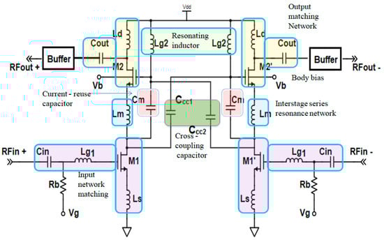
Figure 1.
Schematic of proposed differential LNA.
The interstage series resonance inductor (Lm) serves to eliminate the impact of parasitic capacitance between the common-source (CS) transistor M1 and the cascode transistor M2, thereby enhancing power transfer efficiency. The current-reuse capacitor (Cm) plays a crucial role in augmenting the transconductance (gm2) of the cascode device by enabling the sharing of the input current with the output device.
The cascode transistor operates in a common-gate (CG) configuration, specifically designed to mitigate the impact of parasitic gate–drain capacitance in the common-source (CS) stage. This configuration serves to increase the output impedance and enhance input/output isolation. The inclusion of a drain inductor (Ld) and an output capacitor (Cout) in the cascode stage is carefully engineered to achieve the desired output matching.
To strike a balance between bandwidth and gain, several aspects are addressed, including the transistor sizes, input/output matching networks, the addition of a buffer at the output side, and the incorporation of feedback components. These measures are meticulously executed to attain the desired gain and bandwidth characteristics while ensuring system stability.
To enhance linearity, cross-coupling capacitors CCC1 and CCC2 are incorporated. These capacitors resonate with the gate inductor (Lg2), effectively canceling out the nonlinearity associated with the common-source (CS) transistor (M1).
To further optimize performance, body biasing is employed by connecting the supply voltage (Vb) to the bulk terminal of cascode transistor M2. This adjustment reduces the threshold of M2, preventing it from entering the weak inversion region and, consequently, reducing power consumption, especially at lower supply voltages.
The designed LNA underwent extensive simulations using EDA tools to validate its performance within the C band.
2.1. Small-Signal Equivalent of the Proposed Differential LNA
Figure 2 depicts the small-signal equivalent model of the proposed differential LNA. This model serves as the basis for the study of gain, linearity, and power optimization. Additionally, when viewed as a two-port network, it provides insight into the input and output impedance characteristics.
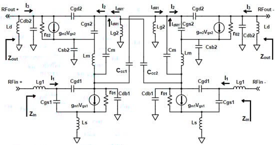
Figure 2.
Small-signal equivalent circuit of proposed LNA.
2.1.1. Gain Improvement Using Current-Reuse Technique
Gain improvement is assessed by analyzing the overall current gain of the proposed LNA. This gain is determined using the small-signal equivalent circuit illustrated in Figure 3.
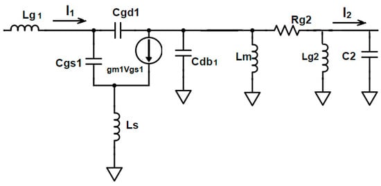
Figure 3.
Small-signal equivalent of input CS stage.
The overall current gain (AI) of the proposed differential LNA can be calculated from the current gain of M1 (I2/I1) and M2 (I3/I2):
The MOS transistors (M1 and M2) are operated in the saturation region with a large voltage headroom to achieve a high gain at the cost of power dissipation. Here, the current-reuse technique is used to boost the current gain of the proposed LNA with low power via the presence of ‘Cm’.
In Figure 3, the current gain of CS transistor M1 is given by
where
Lm is the interstage matching inductor; Lg2 is the gate inductor of M2;
Cdb1 is the drain-to-bulk capacitance of M1;
Rg2 is the gate resistance of M2;
C2 = .
This is the equivalent capacitance composed of interstage capacitance Cm, the gate-to-source capacitance of M2, Cgs2, and cross-coupling capacitor CCC2 obtained from the small-signal equivalent circuit shown in Figure 2 and Figure 4.
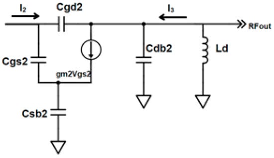
Figure 4.
Small-signal equivalent of cascode stage.
In Figure 4, The current gain of cascode transistor M2 is given by
The current gain (AI) of the differential cascode LNA with gm boosting is achieved from the individual current gain of CS and cascode LNA.
On substituting Equation (2) and (3) in Equation (1), the current gain is
From the current gain expression of AI in Equation (4), it is clear that the gain is boosted twice by the presence of the product of transconductances (gm1 andgm2). Thus, the current gain is improved using the current-reuse capacitor (Cm) under the same DC current with low power.
2.1.2. LNA Linearity Improvement Using Capacitor Cross-Coupling Technique
The CCC technique [35] enhances the linearity of LNA while reducing the gate–drain capacitance of the input common-source (CS) transistor, M1. To achieve a higher IIP3 (third-order input intercept point), it is imperative to minimize gm3, the nonlinear coefficient of M1.
In our proposed approach, to enhance IIP3, we utilize cross-coupling capacitors, CCC1 and CCC2, as illustrated in Figure 1, to mitigate the nonlinear effect of gm3. The gate inductor, Lg2, which is connected to the gate of the cascode transistor, resonates with the cross-coupled capacitors, effectively eliminating the nonlinearity and noise contribution of the cascode stage.
The impact of CCC, which improves the linearity, can be studied using a variation inthe drain current Id of the MOS device given by the Taylor series as
where
Id = gm1vgs + gm2vgs2 + gm3vgs3
gm1 is the main transconductance of the MOSFET;
gm2 is the second-order nonlinear coefficient;
gm3 is the third-order nonlinear coefficient.
The coefficients gm1, gm2, and gm3 are given by
From the above given Equation (6), it is evident that the MOS device exhibits nonlinear behavior.
The IIP3 of the nonlinear device is given by
From Equation (5), the drain currents flowing through M1 and M1′ are given by
where VgsM2 is the gate-to-source voltage of M2 given by
IdM1 = gm1M1vgsM1 + gm2M1vgsM2 + gm3M1vgsM13
IdM1′ = gm1M1′vgsM2 + gm2M1′vgsM22 + gm3M1′vgsM23
VgsM2 = a1vgsM1 + a22 vgsM12 + a32 vgsM13
The resulting current, I2,is given by
I2 = IdM1 + IdM1′
≈(gm1M1 + a1 gm1M1′) vgsM1 + (gm2M1 + a12 gm2M1′) vgsM12 + (gm3M1 + a13 gm3M1′) vgsM13
I2 ≈ gm1M1 + a1 gm1M1′
In Equation (12), it is important to note that gm3M1 and gm3M1′ are negative when operating in the strong inversion region for NMOS transistors. Coefficient a1, representing the impedance when looking at the gate of M2, is a frequency-dependent parameter and is inherently negative according to basic circuit theory [36]. The coefficient of the third term in Equation (12) is offset by adjusting the gate bias of M2 and by resonating the gate inductor Lg2 with the cross-coupling capacitors (CCC1 and CCC2).
Consequently, the resulting current, as given in Equation (13), demonstrates that the nonlinearity components related to gm3 are effectively canceled at M1, allowing the primary transconductance to be directed toward M2.
2.1.3. Transconductance Improvement with Low-Power Body Biasing Technique
Typically, the body of an MOS transistor operates in the weak inversion region. Through the utilization of the forward body biasing technique, the MOS transistor’s body is biased to transition into the strong inversion region. This transition effectively reduces the threshold voltage (VTH) of the device, subsequently leading to a decrease in power consumption. This reduction in the threshold voltage significantly enhances the transconductance (gm), as demonstrated in Equation (14). The following equations describe the variation in gm with VTH:
where
VTH0 is the threshold voltage without the bulk-source voltage.VBS = 0.
Γ is a process-dependent body effect parameter.
is the substrate Fermi potential with typical values of 0.3−0.4V1/2.
n is the substrate factor, whose value depends on the process and varies from 1 to 2.
UT is defined as kT/q, the thermal voltage.
As inferred from the above Equation (14), gm varies exponentially with respect to VTH. Biasing the body of the M2 transistor reduces the threshold voltage and increases transconductance gm2. With the increase in gm2, gain is also proportionally enhanced, as discussed in Equation (4), with a low power consumption.
2.2. Impedance Calculation at Input and Output
Using the small-signal equivalent circuit shown in Figure 2, the input impedance of the proposed differential LNA is given by
where
gm1 is the transconductance of M1; Cgs1 is the parasitic gate-to-source capacitance of gainM1; and Lg1 and Ls are the gate and source inductances.
Input matching is achieved by equating the real part of Equation (16) to source impedance (Rs = 50 Ω) and the imaginary part to zero to obtain the values of the source and gate inductors.
The output frequency (f0) of the proposed LNA can be calculated using
The impedance seen at the output is given by
where
Ld is the drain inductor;
Cdb2 is the drain-to-bulk capacitance of M2.
3. Development of ANN Model
Neural networks are information processing systems designed with inspiration from the cognitive capabilities of the human brain. These networks abstractly generalize and learn from data, drawing upon their capacity to interpret patterns. An ANN model is capable of estimating various amplifier parameters based on simulation results, offering an alternative approach to traditional simulation tools.
Neural Network Model for the Proposed CMOS Differential LNA
The proposed LNA is meticulously designed, incorporating current-reuse, body biasing, and capacitor coupling techniques to achieve optimized gain, a low power consumption, improved linearity, and reduced noise. The key performance parameters, including S-parameters and the noise figure (NF), exhibit proportional variations with temperature across different frequencies. Consequently, both temperature and frequency are considered as input variables. The output parameters, S21 and NF, serve as the output variables in the modeling of the proposed LNA, as depicted in Figure 5.
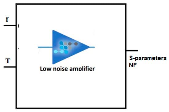
Figure 5.
Parameters considered for neural network modeling of the proposed LNA.
A flowchart for the modeling of the LNA using ANN is illustrated in Figure 6. The proposed LNA is simulated through Cadence, and performance parameters are obtained for various combinations of temperature and frequency. For each set of circuit parameters, the S-parameters and noise figure (NF) are determined, and the corresponding input dataset is generated.In line with the Pareto principle, the developed dataset is partitioned, with 80% allocated for training and the remaining 20% for testing and validation purposes. The ANN is then trained using different numbers of hidden neurons across various neural networks and algorithms. The model’s performance is subsequently validated based on the accuracy achieved through the best test statistics.
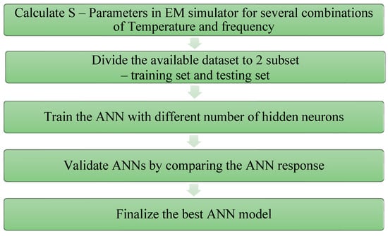
Figure 6.
Flowchart of ANN modeling of the proposed LNA.
An MLPNN model is developed for the proposed LNA, as shown in Figure 7, for the S-parameters and noise figure (NF).
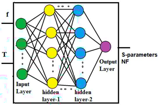
Figure 7.
Neural network model developed for the proposed LNA.
Each ANN is equipped with input neurons that correspond to specific circuit parameters, as well as an output neuron that corresponds to the parameter being modeled. Once the ANN is trained, the desired parameter can be readily calculated based on its response. The model’s accuracy is validated by comparing the ANN’s response with the simulation results.
Specialized versions of feedforward networks, such as PatternNet, FitNet, and Cascade ForwardNet, are available and suitable for various types of input-to-output mapping. Consequently, these networks are chosen to explore the different ANN types while examining the impact of varying the number of hidden layers (NHL) on output accuracy. These neural networks are trained using various algorithms, as listed in Table 1.

Table 1.
Different neural network algorithms.
Bayesian regularization is proposed for modeling this LNA. Typically, the dataset is partitioned into three subsets: training, testing, and validation. The training set error steadily decreases as the training progresses, while the validation set error initially reaches a minimum and then increases as the training continues. This phenomenon can lead to a less predictive model, and it is commonly referred to as overtraining. To overcome this issue, Bayes’ theorem is incorporated into the regularization scheme.
The cost function or sum squared error in the data to be minimized is given as
where
Nd is the number of rows in the input vector X;
Nw is the number of weights;
Xi is the input vector;
Yi is the output vector.
Given the initial values of hyperparameters α and , the cost function S(w) is minimized with respect to weights w.
4. Results and Discussion
The proposed differential LNA was designed and simulated using 180 nm CMOS technology, operating at a frequency of 5 GHz, as depicted in Figure 8. The simulation was carried out within the Cadence Spectre environment. Square spiral inductors and capacitors from the technology library available in Cadence Spectre were utilized. For signal lines, Metal 6 was employed to ensure high conductivity, while input and output lines were implemented using Metal 4 to achieve good impedance matching. Intermediate connections were established using Metal 1 and Metal 2. To enhance signal transmission, the gain path of the proposed LNA was widened to reduce resistance effectively. The component values for the proposed LNA are provided in Table 2. The physical footprint of the proposed LNA occupies a silicon area measuring 0.8 × 0.6 mm2. A process corner analysis was conducted at various temperatures:Typical-Typical (TT, 27 °C), Fast-Fast (FF, 0 °C), and Slow-Slow (SS, 80 °C).
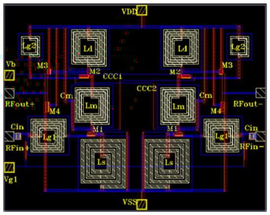
Figure 8.
Layout of proposed differential LNA.
Table 2.
Component values of the proposed LNA.
4.1. Effect of Body Biasing and Current-Reuse Technique on LNA Gain
Figure 9 illustrates the gain improvement (S21) as the bulk voltage (Vb) is varied from −0.3 V to 0.3 V. Notably, it is observed that the gain of the proposed LNA reaches 29.5 dB at the bulk voltage of Vb = −0.3 V. Furthermore, it can be inferred that the gain within the frequency range of 4.9 GHz to 5 GHz measures 29 dB, highlighting its exceptional performance in comparison to previously reported designs [6,8].
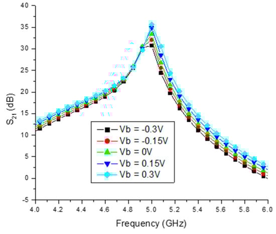
Figure 9.
Body bias (Vb) vs. gain (S21) of differential LNA.
The current-reuse (CR) technique is applied using the middle capacitor, Cm. As Cm is varied from 100 fF to 500 fF, the gain demonstrates an improvement, increasing from 28.8 dB to 33.2 dB, as depicted in Figure 10. It is evident in the figure that the maximum gain is achieved when Cm equals 200 fF at the desired frequency of 5 GHz. Consequently, the gain is enhanced twofold through the combined use of the body biasing (BB) and CR techniques, in accordance with Equation (14).
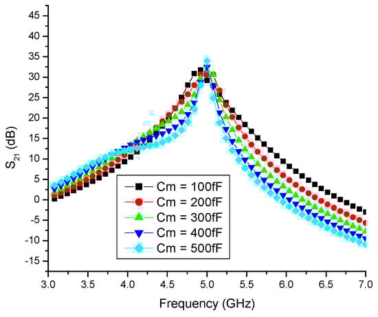
Figure 10.
Current-reuse capacitor (Cm) vs. gain (S21)of differential LNA.
4.2. Effect of Capacitor Cross-Coupling on LNA Linearity
The linearity of the LNA is assessed through the third-order input intercept point (IIP3). In receiver LNAs, it is expected that the IIP3 should exceed −10 dBm. The IIP3 of the proposed LNA is determined through simulation using a two-tone signal with a 100 MHz spacing. As depicted in Figure 11, the proposed LNA achieves an IIP3 of 0.2 dBm with capacitor cross-coupling and −13.3 dBm without capacitor cross-coupling. Consequently, the utilization of the CCC technique results in a significant improvement of 13 dBm.
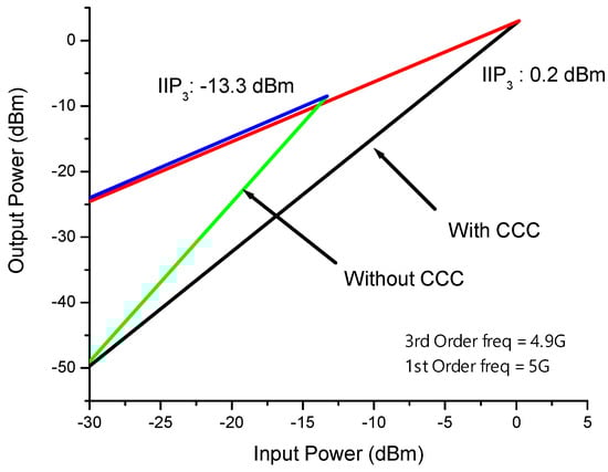
Figure 11.
IIP3 of proposed LNA.
4.3. Simulation Results at Different Process Corners
Figure 12 presents the simulation results of the differential LNA under different process corners. Notably, it is observed that the proposed differential LNA delivers superior performance at the Fast corner (0 °C) when compared to the Typical (27 °C) and Slow corners (80 °C). The gain of the proposed LNA under different corners is illustrated in Figure 12a. It is evident that the gain exceeds 25 dB within the operational bandwidth (4.8–5.2 GHz) and reaches 30 dB at the desired frequency. Furthermore, it is noteworthy that the gain remains consistent between the Typical and Fast corners.
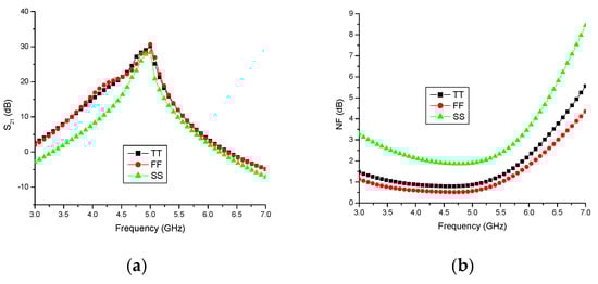
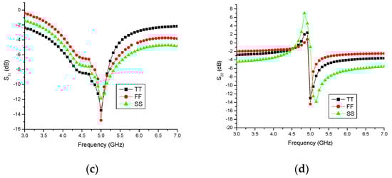
Figure 12.
Simulation results at different process corners: (a) gain (S21), dB; (b) noise figure (NF), dB; (c) input return loss (S11), dB; and (d) output return loss (S22), dB.
The noise figure (NF) of the LNA must be below 3 dB within the desired frequency range. Figure 12b depicts the NF at various corners, revealing an NF of 1.2 dB at the Typical corner, 0.7 dB at the Fast corner, and 1.95 dB at the Slow corner for the desired frequency. These results signify that the noise performance is excellent at the Fast corner.
In terms of the input return loss (S11), it is imperative that it remains below −10 dB at the required frequency of operation. Figure 12c shows that S11 measures−13.3 dB at the Typical corner, −14.5 dB at the Fast corner, and −12.1 dB at the Slow corner within the desired frequency range. This indicates that S11 is particularly strong at the Fast corner when compared to the SS and TT corners.
Similarly, the output return loss (S22) should also be less than −10 dB at the required frequency of operation. As illustrated in Figure 12d, S22 is −13.1 dB at the Typical corner, −14.8 dB at the Fast corner, and −11.3 dB at the Slow corner within the desired frequency range. Additionally, the results suggest that the output return loss is nearly consistent between the Typical and Fast corners.
The performance parameters such as gain, NF, input and output return loss, and power dissipation at various process corners are analyzed and tabulated in Table 3.
Table 3.
Performance of the proposed LNA in normal, best, and worst cases at 5 GHz.
4.4. Performance Comparison of Proposed LNA with Existing State of Art
The performance of the proposed LNA is compared to that of several previously reported differential LNAs designed for wireless applications, and the results are summarized in Table 4. The proposed LNA achieves a gain of 29.5 dB, a noise figure of 1.2 dB, and an IIP3 of 0.2 dBm, all while operating at a reduced supply voltage of 0.9 V. These results outperform the reported works [6,7,8].
Table 4.
Performance summary with existing state of the art LNAs.
It is noteworthy that the proposed LNA exhibits a Figure of Merit (FoM) of 24.26, which is notably higher than in all the other reported works. The advantages brought by the proposed design techniques, such as the body-biased differential architecture combined with current reuse and capacitor cross-coupling, are evident, especially in achieving a highly linear and low-power solution.
The Figure of Merit (FoM) is calculated using Equation (24):
4.5. Performance Comparison with Different NN Models
This section can be divided into two parts. Figure 10 illustrates the impact of temperature on the S-parameters and noise figure (NF) for the frequency obtained from the Cadence simulations. ANN models were constructed for the CMOS differential LNA with 2 input neurons, 25 hidden neurons, and 2 output neurons. These models were trained using 750 datasets, employing 13 different neural network algorithms to identify high efficiency and performance rates. The performance rate varied across the different neural networks, and the best-performing neural network was subsequently analyzed.
Table 5 presents a performance comparison of the various neural networks developed for the proposed CMOS differential LNA. ANN training was carried out using different neural networks while keeping the number of hidden layers constant. It was observed that PatternNet, FitNet, and CascadeForwardNet consistently achieved accuracy levels exceeding 99% when utilizing 25 hidden neurons in the BR algorithm.
Table 5.
Percentage accuracy obtained with different neural networks for the proposed LNA.
Table 6 displays the Mean Relative Error (MRE) and Root Mean Square Error (RMSE) for various algorithms implemented with PatternNet. Based on the results obtained, the PatternNet-BR algorithm exhibits a lower MRE, making it the preferred choice for our LNA modeling.
Table 6.
MRE and RMSE for different algorithms of PatternNet.
Table 7 presents the accuracy achieved using the BR algorithm with different neural networks and various numbers of hidden layers, including 5, 10, 25, and 30 neurons. The results indicate that an accuracy of over 99% was consistently achieved with the neural networks with 25 to 30 neurons for the modeling of this LNA.
Table 7.
Accuracy obtained for BR algorithm with different numbers of hidden neurons.
4.6. Performance Comparison between Cadence Simulation and Developed ANN Results
To account for temperature variations ranging from 0 °C to 80 °C, the LNA parameters are compared between the results from the Cadence simulations and those from ANN.
Table 8 and Table 9 provide sample training and testing data, along with the results obtained from the Cadence simulations and ANN modeling. These tables illustrate that the S-parameters and NF values for the proposed LNA are nearly identical to the results obtained through the ANN modeling. Each sample number corresponds to a specific frequency (in GHz) for a given temperature (in degrees).
Table 8.
Sample training data and the results obtained from Cadence and ANN.
Table 9.
Sample testing data and the results obtained from Cadence and ANN.
Figure 13 presents a comparison between the Cadence simulations and the results generated through the ANN modeling for the CMOS differential LNA parameters. The observation indicates that the results for the proposed LNA are almost identical.
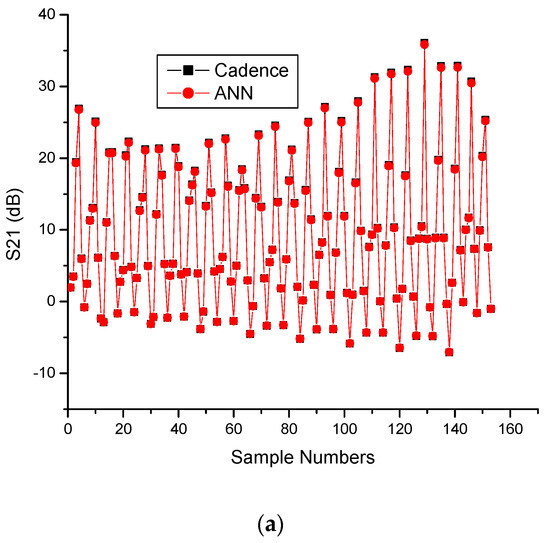
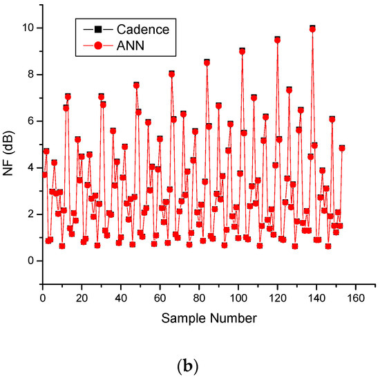
Figure 13.
CMOS differential LNA results obtained using Cadence and ANN: (a) S21, (b) NF.
5. Performance Comparison with the Existing State of Art
Table 10 provides a performance comparison with the existing state of the art. It is evident that the proposed LNAs are modeled using the MLPNN–BR algorithm, which proves to be more robust than the standard back-propagation method. This algorithm also demonstrates the ability to uncover potentially complex relationships, even when the data are limited; requires less formal statistical training; reduces or eliminates the need for extensive cross-validation; and prevents over-fitting. This comparison is made against the reported works [37,38,44,45,46].
Table 10.
Performance comparison with the existing state of the art.
6. Conclusions
This paper introduces Artificial Neural Network (ANN) modeling of a proposed LNA, which is a CMOS differential LNA designed to enhance gain, linearity, and power efficiency. The adaptation of the capacitor cross-coupling technique involves the use of cross-coupling capacitors alongside the gate inductor of the cascode device to resonate the nonlinear component found in the CS stage while allowing the main transconductance to reach the output. Gain is increased through the implementation of the CR and BB techniques, all while maintaining a low power consumption. The proposed LNA achieves remarkable results with a 29.5 dB gain, a 1.2 dB NF, and an IIP3 of 0.2 dBm, all with a reduced supply voltage of 0.9 V.
It is evident that this LNA exhibits a high gain, a low NF, and excellent linearity at the desired frequency, even with a reduced supply voltage. The modeling of the proposed LNA using PatternNet BR reveals that the simulation results closely match those of the developed ANN. When compared with the Cadence simulation method, the proposed technique can also provide precise circuit solutions. While simulation or measurement data may be used for modeling, the proposed method’s advantages are more pronounced, especially in cases where equivalent circuits for simulation are unavailable or when measurements are costly.
Author Contributions
Conceptualization, B.S. and J.K.; methodology, V.T. and V.B.; software, B.S.; validation, V.B. and U.M.P.; formal analysis, B.S.; investigation, B.S.; writing—original draft preparation, B.S., V.T. and V.B.; writing—review and editing, U.M.P. and J.K.; visualization, V.T.; supervision, J.K. All authors have read and agreed to the published version of the manuscript.
Funding
This research received no external funding.
Data Availability Statement
All data are included within manuscript.
Acknowledgments
The authors would like to thank The Management, The Principal and Head of the Department of ECE, Mangayarkarasi College of Engineering who gives their full support for our work.
Conflicts of Interest
The authors declare no conflict of interest.
References
- Kim, T.-S.; Kim, B.-S. Post-Linearization of Cascode CMOS Low Noise Amplifier Using Folded PMOS IMD Sinker. IEEE Microw. Wirel. Compon. Lett. 2006, 16, 182–184. [Google Scholar]
- Lee, T.H. The Design of CMOS Radio Frequency Integrated Circuits; Cambridge University Press: Cambridge, UK, 2000. [Google Scholar]
- Woo, S.; Kim, W.; Lee, C.H.; Kim, H.; Laskar, J. A Wideband Low-Power CMOS LNA With Positive–Negative Feedback forNoise, Gain, and Linearity Optimization. IEEE Trans. Microw. Theory Tech. 2012, 60, 3169–3178. [Google Scholar] [CrossRef]
- Alam, S.K.; DeGroat, J. A 2 GHz variable gain low noise amplifier in 0.18-μm CMOS. Analog Integr. Circ. Sig. Process. 2008, 56, 37–42. [Google Scholar] [CrossRef]
- Fan, X.; Zhang, H.; Sánchez-Sinencio, E. A Noise Reduction and Linearity Improvement Technique for a Differential Cascode LNA. IEEE J. Solid-State Circuits 2008, 43, 588–599. [Google Scholar] [CrossRef]
- Cen, M.; Song, S. A Differential Cascode Low Noise Amplifier Based on a Positive Feedback Gain Enhancement Technique. J. Mach. Mach. Commun. 2015, 1, 229–244. [Google Scholar] [CrossRef]
- Kalamani, C. Design of Differential LNA and Double Balanced Mixer using 180nm CMOS Technology. Microprocess. Microsyst. 2019, 71, 102850. [Google Scholar] [CrossRef]
- Wang, W.; Wang, C. Capacitor Cross-Coupled Fully differential CMOS Folded Cascode LNAs with Ultra Low Power Consumption. Wirel. Pers. Commun. 2014, 78, 45–55. [Google Scholar] [CrossRef]
- Muhamad, M.; Soin, N.; Ramiah, H.; Noh, N.M.; Chong, W.K. Design of CMOS differential LNA at 2.4 GHz. In Proceedings of the 2013 IEEE International Conference of Electron Devices and Solid-State Circuits, Hong Kong, China, 3–5 June 2013. [Google Scholar]
- Kumar, M.G.L.; Regulagadda, S.S.; Das, J.K.; Dutta, A. Design of Current Reuse based Differential Merged LNA-Mixer (DMLNAM) and Two-stage Dual Band LNA with two Gain modes in 65 nm technology. In Proceedings of the 2015 IEEE Asia Pacific Conference on Postgraduate Research in Microelectronics and Electronics, Hyderabad, India, 27–29 November 2015; pp. 98–103. [Google Scholar]
- Kargaran, E.; Mafinejad, Y.; Mafinezhad, K.; Nabovati, H. A new gm boosting current reuse folded cascode LNA. IEICE Electron. Express 2013, 10, 20130264. [Google Scholar] [CrossRef]
- Shankar, S.U.; Dhas, M.D.K. Design and Performance Measure of 5.4 GHZ CMOS Low Noise Amplifier using Current ReuseTechnique in 0.18μmTechnology. Procedia Comput. Sci. 2015, 47, 135–143. [Google Scholar] [CrossRef][Green Version]
- Dai, R.; Zheng, Y.; He, J.; Liu, G.; Kong, W.; Zou, S. A 0.5-V novel complementary current-reused CMOSLNAfor 2.4 GHz medical application. J. Microelectron. 2016, 55, 64–69. [Google Scholar] [CrossRef]
- Chang, C.-H.; Onabajo, M. Analysis and Demonstration of an IIP3 Improvement Technique for Low-Power RF Low-Noise Amplifiers. IEEE Trans. Circuits Syst. I Regul. Pap. 2018, 65, 859–869. [Google Scholar] [CrossRef]
- Liu, H.J.; Zhang, Z.F. An Ultra-Low Power CMOS LNA for WPAN Applications. IEEE Microw. Wirel. Compon. Lett. 2017, 27, 174–176. [Google Scholar] [CrossRef]
- Fiorelli, R.; Silveira, F.; Peralias, E. MOST moderate weak inversion region as the optimum design zone for CMOS 2.4-GHz CS-LNAs. IEEE Trans. Microw. Theory Tech. 2014, 62, 556–566. [Google Scholar] [CrossRef]
- Li, C.-H.; Liu, Y.-L.; Kuo, C.-N. A 0.6-V 0.33-mW 5.5-GHz receiver front-end using resonator coupling technique. IEEE Trans. Microw. Theory Tech. 2011, 59, 1629–1638. [Google Scholar] [CrossRef]
- Lai, M.-T.; Tsao, H.-W. Ultra-Low Power Cascaded CMOS LNA With Positive Feedback and Bias Optimization. IEEE Trans. Microw. Theory Tech. 2013, 61, 1934–1945. [Google Scholar] [CrossRef]
- Singh, V.; Arya, S.K.; Kumar, M. A 0.7V, Ultra-Wideband Common Gate LNA with Feedback BodyBias Topology for Wireless Applications. J. Low Power Electron. Appl. 2018, 8, 42. [Google Scholar] [CrossRef]
- Wang, T.-P. Minimized Device Junction Leakage Current at Forward-Bias Body and Applications for Low-Voltage Quadruple-Stacked Common-Gate Amplifier. IEEE Trans. Electron Devices 2014, 61, 1231–1236. [Google Scholar] [CrossRef]
- Zhang, H.; Sánchez-Sinencio, E. Linearization Techniques for CMOS Low Noise Amplifiers: A Tutorial. IEEE Trans. Circuits Syst. I Regul. Pap. 2011, 58, 22–36. [Google Scholar] [CrossRef]
- Kargaran, E.; Mafinejad, Y.; Mafinezhad, K.; Nabovati, H. Highly Linear Folded Cascode LNA. IEICE Electron. Express 2013, 10, 20130557. [Google Scholar] [CrossRef]
- Aparin, V.; Larson, L.E. Linearization of monolithic LNAs using low-frequency low-impedance input termination. In Proceedings of the 29th European Solid-State Circuits Conference, Estoril, Portugal, 16–18 September 2003; pp. 137–140. [Google Scholar]
- Aparin, V.; Brown, G.; Larson, L.E. Linearization of CMOS LNAs via optimum gate biasing. In Proceedings of the 2004 IEEE International Symposium on Circuits and Systems, Vancouver, BC, Canada, 23–26 May 2004; pp. 748–751. [Google Scholar]
- Lou, S.; Luong, H.C. AlinearizationtechniqueforRFreceiverfront-endusingsecond-orderintermodulationinjection. IEEE J. Solid-State Circuits 2008, 43, 2404–2412. [Google Scholar] [CrossRef]
- Jin, T.H.; Kim, T.W. A 5.5-mW +9.4-dBm IIP3 1.8dB NF CMOS LNA Employing Multiple Gated Transistors with Capacitance Desensitization. IEEE Trans. Microw. Theory Tech. 2010, 58, 2529–2537. [Google Scholar] [CrossRef]
- Kim, Y.M.; Han, H.; Kim, T.W. A 0.6-V +4dBm IIP3 LC folded cascode CMOS LNA with gm linearization. IEEE Trans. Circuits Syst. II Express Briefs 2013, 60, 122–126. [Google Scholar]
- Salim, Z.Z.M.; Muhamad, M.; Hussin, H.; Ahmad, N. CMOS LNA Linearization Employing Multiple Gated Transistors. In Proceedings of the 2019 IEEE International Conference on Telecommunication Systems, Services, and Applications (TSSA), Bali, Indonesia, 3–4 October 2019. [Google Scholar]
- Ma, L.; Wang, Z.-G.; Xu, J.; Amin, N.M. A High Linearity Wideband Common-Gate LNA with Differential Active Inductor. IEEE Trans. Circuits Syst. II Express Briefs 2017, 64, 402–406. [Google Scholar] [CrossRef]
- Kumaravel, S.; Kukde, A.; Venkataramani, B.; Raja, R. A high linearity and high gain Folded Cascode LNA for narrow band receiver applications. Microelectron. J. 2016, 54, 101–108. [Google Scholar] [CrossRef]
- Tarighat, A.P.; Yargholi, M. A CMOS low noise amplifier with employing noise cancellation and modified derivative superposition technique. Microelectron. J. 2016, 54, 116–125. [Google Scholar] [CrossRef]
- Raja, R.; Venkataramani, B.; Kishore, K.H. A 1-V 2.4 GHz Low-Power CMOS LNA Using Gain-Boosting and Derivative Superposition Techniques for WSN. Wirel. Pers. Commun. 2017, 96, 383–402. [Google Scholar] [CrossRef]
- Rafati, M.; Qasemi, S.R.; Amiri, P. A 0.65V, linearized cascade UWB LNA by application of modified derivative superpositiontechnique in 130nm CMOS technology. Analog Integr. Circuits Signal Process. 2019, 99, 693–706. [Google Scholar] [CrossRef]
- Chang, C.-P.; Chien, W.-C.; Su, C.-C.; Wang, Y.-H.; Chen, J.-H. Linearity improvement of cascode CMOS LNA using a diode connected NMOS transistor with a parallel RC circuit. Prog. Electromagn. Res. C 2010, 17, 29–38. [Google Scholar] [CrossRef]
- Guo, B.; Chen, J.; Jin, H. A linearized common-gate low-noise amplifier using active cross-coupled feedback technique. Analog Integr. Circuits Signal Process. 2016, 89, 239–248. [Google Scholar] [CrossRef]
- Wu, Y.; Kim, H.; Jonsson, F.; Ismail, M.; Olsson, H. Nonlinearity Analysis of a Short Channel CMOS Circuit for RFIC Applications. In VLSI: Systems on a Chip; IFIP International Federation for Information Processing; Silveira, L.M., Devadas, S., Reis, R., Eds.; Springer: Boston, MA, USA, 1999; Volume 34, pp. 61–68. [Google Scholar]
- Sorkhabi, S.E.; Mosavi, M.R.; Rafei, M. Low Noise amplifier synthesis using multidimensional MLP neural network. IETE J. Res. 2018, 64, 374–386. [Google Scholar] [CrossRef]
- Kumar, S.; Kumari, S. Design of low power, high gain LNA for WCDMA range and parameters extraction using Artificial Neural Network (ANN). In Proceedings of the 2015 IEEE Power, Communication and Information Technology Conference (PCITC), Bhubaneswar, India, 15–17 October 2015. [Google Scholar] [CrossRef]
- Güneş, F.; Çağlar, M.F. A Novel Neural Smith Chart for use in Microwave circuitry. Int. J. RF Microw. Comput. Eng. 2008, 19, 218–229. [Google Scholar] [CrossRef]
- Gorissen, D.; De Tommasi, L.; Crombecq, K.; Dhaene, T. Sequential modeling of a low noise amplifier with neural networks and active learning. Neural Comput. Appl. 2009, 18, 485–494. [Google Scholar] [CrossRef]
- Karimi, G.; Sedaghat, S.B.; Banitalebi, R. Designing and modeling of ultra-low voltage and ultra-low power LNA using ANN and ANFIS for Bluetooth applications. Neurocomputing 2013, 120, 504–508. [Google Scholar] [CrossRef]
- Dumesnil, E.; Nabki, F.; Boukadoum, M. RF-LNA circuit synthesis using an array of artificial neural networks with Constrained Inputs. In Proceedings of the 2015 IEEE International Symposiumon Circuits and Systems (ISCAS), Lisbon, Portugal, 24–27 May 2015; pp. 573–576. [Google Scholar] [CrossRef]
- Singh, S.; Chopra, P.K. Artificial Neural Network approach for LNA design of GPS receiver. Opt. Mem. Neural Netw. 2016, 25, 236–242. [Google Scholar] [CrossRef]
- Güneş, F.; Demirel, S.; Nesil, S. Design optimization of LNAs and reflect array antennas using the full-wave simulation-based artificial intelligence models with the novel metaheuristic algorithms. In Simulation-Driven Modeling and Optimization; Springer Proceedings in Mathematics & Statistics; Koziel, S., Leifsson, L., Yang, X.S., Eds.; Springer: Cham, Switzerland, 2016; Volume 153. [Google Scholar] [CrossRef]
- Payala, A.; Anand, R. Modelling of navigation based LNA parameters using neural network technique. Opt. Mem. Neural Netw. 2017, 26, 192–198. [Google Scholar] [CrossRef]
- Xhafa, X.; Yelten, M.B. Design of a tunable LNA and its variability analysis through surrogate modeling. Int. J. Numer. Model. Electron. Netw. Devices Fields 2020, 33, e2724. [Google Scholar] [CrossRef]


Disclaimer/Publisher’s Note: The statements, opinions and data contained in all publications are solely those of the individual author(s) and contributor(s) and not of MDPI and/or the editor(s). MDPI and/or the editor(s) disclaim responsibility for any injury to people or property resulting from any ideas, methods, instructions or products referred to in the content. |
© 2023 by the authors. Licensee MDPI, Basel, Switzerland. This article is an open access article distributed under the terms and conditions of the Creative Commons Attribution (CC BY) license (https://creativecommons.org/licenses/by/4.0/).