Abstract
In this work, a new versatile voltage- and transconductance-mode analog filter is proposed. The filter, without requiring resistors, employs three differential-difference transconductance amplifiers (DDTAs) and two grounded capacitors, which is suitable for integrated circuit implementation. Unlike previous works, the proposed filter topology provides: (1) high-input and low-output impedances for a voltage-mode (VM) analog filter, that is desirable in a cascade method of realizing higher order filters, and (2) high-input and high-output impedances for a transconductance-mode (TM) analog filter without any circuit modification. Moreover, a quadrature oscillator is obtained by simply adding a feedback connection. Both VM and TM filters provide five standard filtering responses such as low-pass, high-pass, band-pass, band-stop and all-pass responses into single topology. The natural frequency and the condition of oscillation can be electronically controlled. The circuit operates with 0.5 V supply voltage. It was designed and simulated in the Cadence program using 0.18 µm CMOS technology from TSMC.
1. Introduction
The differential difference amplifiers (DDA) are versatile analog building blocks that offer two differential input ports, high-input impedance, and low-output impedance [1,2,3]. If an ideal DDA (infinite open-loop gain) operates in negative feedback configuration, it can work as summing and subtracting amplifier with unity gain. This ability has been used to increase the performance of new devices such as a differential difference current conveyor (DDCC) [4], differential difference current conveyor transconductance amplifier (DDCCTA) [5], or differential difference transconductance amplifier (DDTA) [6]. The properties of DDCC are similar to those of the conventional second-generation current conveyor (CCII) [7] except the input port that offers arithmetic operation. Thus, DDCC-based filters require resistors and its natural frequency cannot be tuned electronically, for example, see [8,9,10,11,12]. To obtain electronic tuning ability, the DDTA has been presented. The DDTA is a cascade connection of DDA and a transconductance amplifier (TA), as shown in Figure 1a, and its electrical symbol is shown in Figure 1b. Compared with DDCCTA, DDTA is more compact. The DDTA provides addition and subtraction of the voltages Vy1, Vy2, Vy3 at the w-terminal, namely, Vw = Vy1 − Vy2 + Vy3. This terminal usually provides low-impedance level (results from negative feedback of DDA), which is suitable for output terminals of voltage-mode circuits. The o-terminal provides output current which is the product of the differential voltage Vw-Vy4 and the transconductance gm, i.e., Io = gm(Vw-Vy4). Thus, an electronic tuning ability of DDTA can be obtained by tuning . The ideal characteristics of DDTA in Figure 1a can be described by
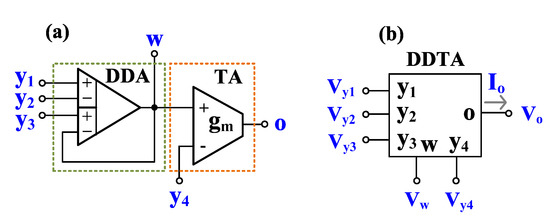
Figure 1.
DDTA, (a) possible realization of DDTA, (b) electrical symbol.
There are many applications of DDTA in the open literature, such as analog filters [13,14,15,16,17,18]. The universal filter in [13] uses DDTA with ±2 V supply and 1.66 mW power consumption. The analog wave filter in [14] uses DDTA with ±1.8 V supply and 21.59 μW power consumption. The mixed-mode universal filter in [15] uses DDTA with 1.2 V supply and 66 μW power consumption. The sub-volt universal filters in [16,17] use DDTAs with 0.5 V supply and 205.5 nW [16] and 277 nW [17] power consumption. Finally, the sub-voltage universal filter in [18] use DDTA with a 0.3 V supply and 357.4 nW power consumption.
Universal analog filters can be applied in telecommunication, electronic, and control systems, performing such functions as rejection of out-of-band noise, attenuation of the unwanted frequency components from the applied signal, realization of the active crossover network, or reduction of noise in a process measurement signal [19,20,21]. Moreover, they can be used to realize high-order filters [22]. In most applications of universal analog filters, voltage-mode analog filters with high-input and low-output impedances are required to avoid additional buffers or loading effects. There are universal analog filters with high-input and low-output impedances available in literature, using alternative active elements such as DDCCs [11,23], fully differential second-generation current conveyors (FDCCII) [24], current-feedback amplifiers (CFA) [25,26,27], universal voltage conveyors (UVC) [28], voltage differencing differential difference amplifier (VDDDA) [29]. However, analog filters based on these active devices in [11,23,24,25,26,27,28] require passive resistors and do not offer electronic tuning ability. The analog filters based on VDDDAs [29] provide an electronic tuning ability, but only voltage-mode filters and seven transfer functions are proposed.
This work proposes a versatile analog filter based on low-voltage differential difference transconductance amplifiers with enhanced performance. The proposed filter topology offers high-input and low-output impedances which is convenient for voltage-mode circuits, as well as many transfer functions of low-pass (LP), high-pass (HP), band-pass (BP), band-stop (BS) and all-pass (AP) filters into same topology. In addition, using the same versatile topology, transconductance-mode filters and a quadrature oscillator can be obtained. TM version provides LP, HP, BP, BS, and AP characteristics with high-input and high-output impedance, that is required of TM circuits. The natural frequency of the filters and the condition of oscillation for oscillator can be electronically controlled. The proposed DDTA and its applications operate with 0.5 V supply and are designed and simulated in the Cadence program using the 0.18 µm CMOS process from TSMC.
2. Proposed Circuit
2.1. 0.5 V DDTA
The CMOS structure of the proposed DDTA is shown in Figure 2. It consists of two main blocks, a differential-difference current conveyor realized with DDA operating in a negative-feedback configuration and TA [16]. The differential-difference amplifier is realized using a non-tailed differential pair M1-M2 [30], which is well suited for low-voltage circuits. However, the input transistors of this pair were replaced by multiple-input bulk-driven transistors (BD MI-MOST), shown in Figure 3. The multiple-input bulk-driven transistors are realized with an additional capacitive voltage divider, consisting of the capacitors CB, shunted by anti-parallel connections of the transistors ML. Note, that ML operate with VGS = 0, thus realizing a very large resistance RLARGE. Their purpose is to provide proper biasing of the input terminals for DC. For frequencies much larger than 1/RLARGECB, the resulting impedance of the RLERGECB connections is dominated by capacitors, and the AC voltage at the bulk terminals of the multiple input transistors can be expressed as:
where, neglecting the impact of the MOS transistors, seen from their bulk terminals, the voltage gain of the input capacitive divider, from i-th input βi, in general case can be expressed as:
where n is the number of inputs. In the proposed design n = 2 and all capacitors CB are equal to each other, then βi = 1/2, for i = 1,2. Denoting the non-inverting and inverting input voltages of the input differential pair as Vi+ and Vi-, respectively, the differential voltage at the bulk terminals of the input non-tailed pair M1A and M1B can be expressed as:
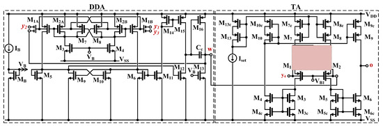
Figure 2.
The CMOS structure of the 0.5 V DDTA.
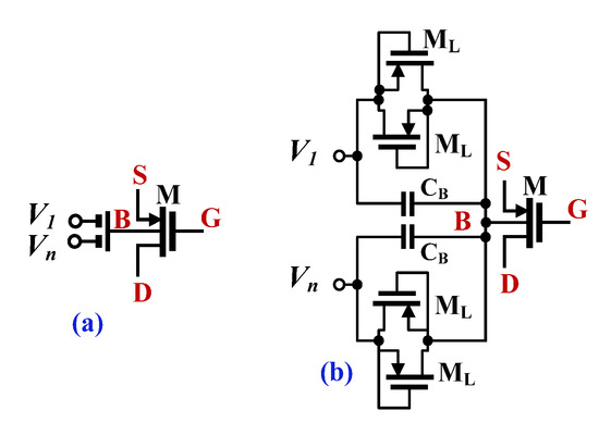
Figure 3.
The symbol of bulk-driven MI-MOST (a) and the CMOS realization (b).
Thus, the AC differential voltage of the “internal” differential pair is a sum of the input differential voltages applied to the capacitive inputs. In such a way, a differential-difference amplifier is realized, using only one transistor structure of the input pair, thus saving the dissipation power and decreasing complexity of the input stage.
Overall, the DDA used in the first block of the proposed DDTA can be seen as a two-stage amplifier, where the first stage can be considered as a current mirror OTA, based on the multiple-input pair, while the second stage, M13-M16, is a typical class-A common source amplifier. The capacitor CC is used for frequency compensation. The two-stage architecture allows increasing the open-loop voltage gain and consequently the accuracy of the realized circuit function. The voltage gain is further increased thanks to the partial-positive feedback (PPF) circuit, realized using two sub-circuits M7-M8 and M9-M10. Each of the cross-coupled pairs of transistors generates negative resistances, thus partially increasing the resulting resistances at the gate/drain nodes of the transistors M2A,B and M5,6 respectively, and consequently increasing the voltage gain of the DDA. However, PPF leads to increased sensitivity of the circuit to transistor mismatch, that can lead to stability problems. This sensitivity, like the voltage gain, increases with the amount of positive feedback, i.e., when the ratio of transconductances gm7,8/gm2A,B (gm9,10/gm5,6) increases towards unity. Therefore, there is a tradeoff between the achieved improvement of the voltage gain and the circuit sensitivity to transistor mismatch. As it was shown in [16], applying two PPF circuits with weaker positive feedback, leads to the same improvement of the voltage gain, with less sensitivity, than applying one PPF circuit providing the same improvement of the gain. Therefore, in the circuit of Figure 2 two PPF circuits have been applied, one connected directly to the input transistors and the second, applied to the load of the input pair.
The open-loop low-frequency voltage gain of the DDA, from one differential input, with the second input grounded for AC signals, can be expressed as [16]:
where Ao is the DC open-loop voltage gain of the DDA without PPF circuits, calculated from the bulk terminals of M1, and given as:
The coefficients m1 and m2 can be expressed as:
The coefficients m1 and m2 can be considered as the ratios of negative to positive conductances in “bottom” and “upper” PPF. In general case, the coefficients can range from zero (lack of positive feedback) to unity (100% positive feedback). The overall voltage gain increases to infinity, as m1 or m2 tends to unity, i.e., as the amount of positive feedback increases. Thanks to the application of two PPFs in the proposed design with m1 = m2 = 0.5, a sufficient increase of the voltage gain (12 dB), with acceptable circuit sensitivity to transistor mismatch was achieved.
The second block of the DDTA in Figure 2 is a transconductance amplifier. In the proposed design, a BD source-degenerative (SD) differential pair, with triode region BD transistors M11 and M12 has been applied, which allows increasing the linear range of the TA by about 3 times, as compared with the conventional BD pair used in [16]. Even better linearity could be achieved using a non-tailed pair with a linear resistor [18,31], but such a solution is not very suitable for transconductors operating in nS range, since it would require very large resistors, not practical in silicon realizations.
For the TA in Figure 2, operating in a weak-inversion region, optimum linearity is achieved if the following condition is satisfied:
where W and L are the transistor channel width and length, respectively. Note, that the above condition is the same as for the gate-driven counterpart of the circuit [32]. For this optimum case, with unity-gain current mirrors, the circuit transconductance gm can be expressed as:
where η = gmb1,2/gm1,2 is the bulk to gate transconductance ratio at the operating point for the input transistors M1 and M2, np is the subthreshold slope factor for p-channel MOS transistors and UT is the thermal potential. As it can be concluded from (11), the circuit transconductance is proportional to the biasing current Iset, thus it can be easily regulated using this current.
2.2. Versatile Analog Filter
The proposed versatile analog filter is shown in Figure 4. The circuit employs only three DDTAs and two grounded capacitors. It should be noted that the output voltages Vo1, Vo2, and Vo3 are defined at the low-impedance w-terminals while the input voltages Vin1 to Vin7 are fed to the high-impedance y-terminals of the DDTA.
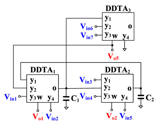
Figure 4.
Proposed voltage-mode analog filter.
Using (1), (2) and nodal analysis, the output voltages of the circuit in Figure 4 can be expressed by
The filtering responses can be obtained by appropriately applying the input signals and choosing the output voltages and the variant filtering responses are shown in Table 1. It should be noted that the VM analog filter provides 34 filtering responses of LP, HP, BP, BS, and AP filters, all of them in both, inverting and non-inverting versions.

Table 1.
Obtaining variant filtering function of voltage-mode analog filter.
Considering denominator of (12)–(14), the natural frequency (ωo) and the quality factor (Q) are given by
The parameter ωo can be controlled electronically by gm1 = gm2 and, in this case, the parameter Q is given by C1/C2.
The VM analog filter in Figure 4 can also operate as transconductance-mode (TM) analog filter, as shown in Figure 5. The output current of the TM filter is the output current of the o-terminal of DDTA3 while the input voltages are same as for the VM filter. The output current of the TM filter is given by
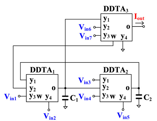
Figure 5.
Modified transconductance-mode analog filter.
The filtering responses can be obtained by appropriately applying the input signals. The variant filtering responses are listed in Table 2. It should be noted that the TM filter provides 11 transfer functions of LP, HP, BP, BS, and AP filters and all filtering responses provide both inverting and non-inverting transfer functions.
Table 2.
Obtaining variant filtering function of transconductance-mode analog filter.
The proposed VM analog filter can be modified to work as a quadrature oscillator as shown in Figure 6. The VM transfer function of a BP filter Vo1/Vin3 is used, with a gain given by
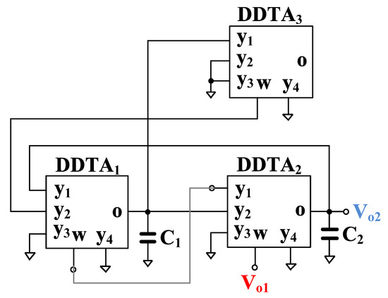
Figure 6.
Modified quadrature oscillator.
Assuming Vo1/Vin3 = 1, the characteristic equation of the oscillator is
assuming further gm1 = gm2, the condition of oscillation is given by
The frequency of oscillation is expressed as
Note, that the frequency of oscillation ωo can be electronically controlled via gm1 and gm2.
Considering nodes Vo1 and Vo2 in Figure 6, we see, that DDTA2 and C2 form a lossless integrator with a transfer function given by
At ω = ωo, the phase and magnitude are given respectively by ∅ = π/2 and |gm2/C2|.
Non-idealities analysis
In non-ideal case, the main equations describing the characteristics of DDTA can be expressed as:
where βk1, βk2, βk3 denote the non-ideal voltage gains from y1, y2 and y3 terminals, respectively, to the w-terminal of the k-th DDTA (βk1 = βk2 = βk3 = 1 in ideal case), gmnk is the frequency-dependent transconductance of the k-th DDTA. At the frequency near the cut-off frequency, gmnk can be approximated by [33]
where μk = 1⁄ωgk, and ωgk denotes the first pole of the k-th DDTA.
Using (23), the output voltages Vo1, Vo2, and Vo3 of the VM analog filter can be rewritten as
Furthermore, the output current Iout of the TM analog filter can be rewritten as
Using (25), the denominators of (26)–(29) can be expressed by
From (30), the parasitic effects from DDTA can be ignored if the following conditions are met
The non-ideal parameters ωo and Q can be expressed as
From the BP function (26), with Vo1/Vin3 = 1, the non-ideal characteristic equation of the oscillator can be expressed by
The condition of oscillations and the frequency of oscillations are:
3. Simulation Results
The circuit was designed and simulated in the Cadence environment using the 0.18 µm CMOS technology form TSMC. The transistors aspect ratios are in Table 3. The voltage supply VDD = 0.5 V and the bias voltage VB1 = −60 mV. For Iset = 5 nA, the total power consumption of the DDTA was 215.5 nW (DDA = 203 nW and TA = 12.5 nW). It is worth mentioning that the DC level on the bulk terminal of the differential pair depends on the DC level of the input signals and on the shunt resistors ML that form a resistor voltage divider [34]. The simulated current of the bulk terminal of the differential pair is less than 0.8% of the input currents in the wholly input range, and hence the current of the bulk terminal could be neglected compared to the inputs one [34]. The value of this input capacitor CB was optimized, based on previous post-layout simulation, to be 0.5 pF, in order to reduce the impact of the parasitic capacitance of the MOS transistor on the circuit performance from one side and to avoid extra increase in chip area from the other side [34,35]. The performance of the MI-MOST was confirmed experimentally in [34,35].
Table 3.
Transistor aspect ratio of the DDTA.
Figure 7 shows the transconductance characteristics versus input voltage of the TA with the proposed SD and without SD that was presented in [16] for Iset = 5 nA. While the transconductance varies by about 10% over the nominal value for the input voltage range of ±40 mV for TA without SD, it is up to ±160 mV for the proposed TA with the SD. Note the improved linearity, obtained thanks to the SD technique.
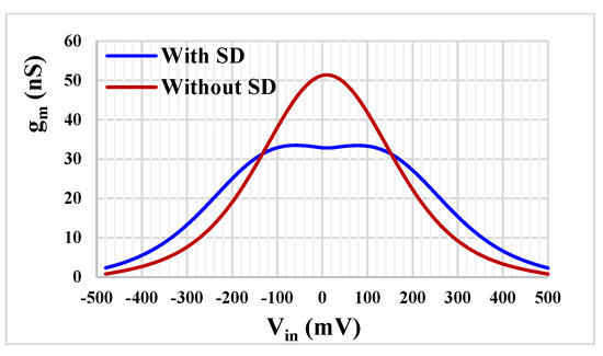
Figure 7.
The transconductance characteristics of the TA with and without SD technique.
The frequency characteristics for the proposed VM filter from Figure 4 are shown in Figure 8. The value of the capacitors were C1 = C2 = 20 pF and the setting current Iset = 5 nA. The −3 dB cut-off frequency for the LP filter was 323.3 Hz.
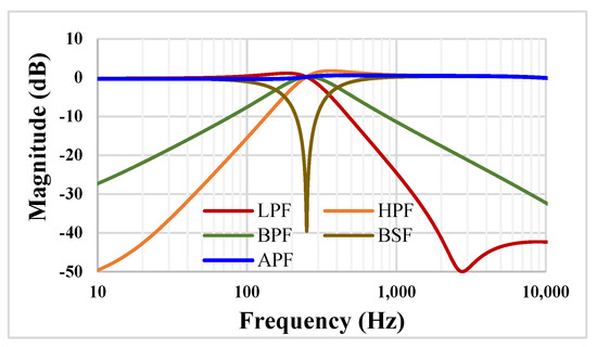
Figure 8.
The frequency characteristics of the VM filter.
The tuning capability for the selected LP and BP filters are shown in Figure 9. With Iset = 2.5 nA, 5 nA, 10 nA, 20 nA the −3 dB frequency of the LPF was 162 Hz, 323.3 Hz, 650.2 Hz and 1.333 kHz, respectively. This, for example, covers a wide spectrum of biosignal filtering applications.
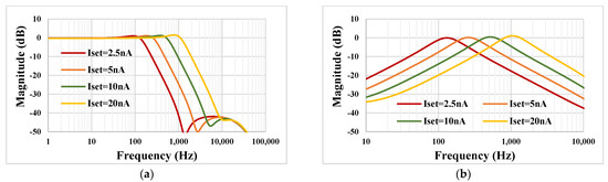
Figure 9.
The simulated frequency characteristics showing the tuning capability of the LP (a) and BP filters (b).
The simulated frequency characteristic of the LP (a) and BP (b) filters with process, voltage, and temperature (PVT) corners are shown in Figure 10. The process corners were fast–fast, fast–slow, slow–fast and slow–slow, the temperature corners were −10 °C and 70 °C, and the voltage supply corners were ±10%VDD. The variation of these characteristics is in acceptable range.
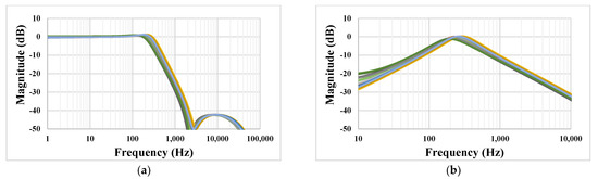
Figure 10.
The simulated frequency characteristic of the LP (a) and BP (b) filters with PVT corners.
The histograms of the −3 dB cut-off frequency and low frequency gain of the LP filter with Monte Carlo (MC) process and mismatch analysis are shown in Figure 11a and Figure 11b, respectively. For the −3 dB cut-off frequency, the mean value was 323.86 Hz and the standard deviation 17.95 Hz, while the mean value of the gain was 432 mdB with a standard deviation of 150.5 mdB. Note that, thanks to the electronic tuning ability of the DDTA, any possible deviation of the filter parameters could be readjusted by the setting current Iset.
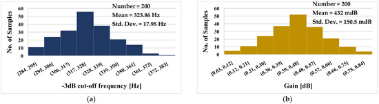
Figure 11.
The histogram of the −3 dB cut-off frequency (a) and low frequency gain (b) of the LPF with 200 MC runs.
The transient response of the LP filter with applied input sine wave signal 100 mVpp @ 10 Hz is shown in Figure 12. The total harmonic distortion (THD) was 0.8%. The output noise of the LPF is shown in Figure 13. The integrated noise value was 108 µV, that results in a dynamic range of 53.2 dB for 1% THD.
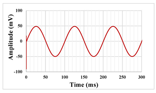
Figure 12.
The transient response of the LP filter.
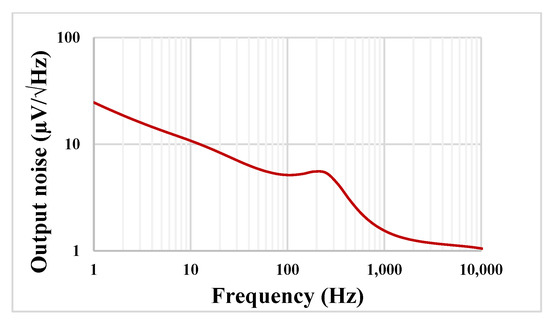
Figure 13.
The output noise the LP filter.
The frequency characteristics for the TM filter from Figure 5 are shown in Figure 14 for same condition as for the VM filter i.e., C1 = C2 = 20 pF and Iset = 5 nA. The low frequency current gain of the LP filter was −150 dB, which corresponds to a transconductance 31.6 nS, and the −3 dB for the LPF was 323.3 Hz.
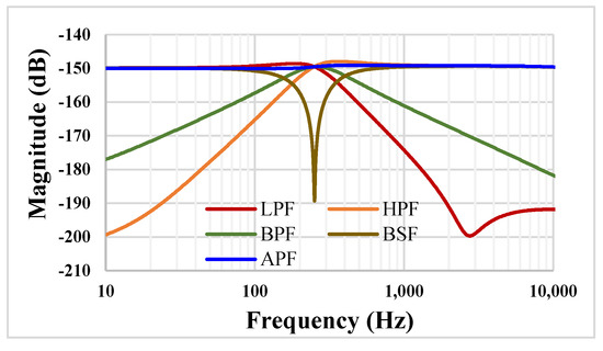
Figure 14.
The frequency characteristics of the TM filter.
The quadrature oscillator in Figure 6 was also simulated with Iset = 5 nA and capacitor values C1 = C2 = 20 pF. Figure 15 shows the starting oscillation (a) and the steady state (b), respectively. The frequency is 253 Hz and the THD was around 1%.
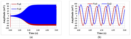
Figure 15.
The starting oscillation (a) and the steady state (b).
Finally, Table 4 provides the performance comparison of this work with others recently published works [11,15,16,18]. This universal filter offers high-input and low-output impedances of VM filter and high-input and high-output impedances of TM filter. Compared with [11,15,16,18], the proposed filters offer 34 transfer functions of VM filter and 11 transfer functions of TIM filters. Compared with [11], the proposed filter provides electronic tuning ability of natural frequency and low-power consumption. Compared with the DDTA-based analog filters in [15,16,17,18], the proposed filter offers the advantages such as low-output impedances which is required for VM circuits, both non-inverting and inverting transfer functions of LP, HP, BP, BS, and AP filters, and maximum VM transfer functions.
Table 4.
Performance comparison of this work with those of recently published.
4. Conclusions
This paper presents a voltage-, transconductance-mode analog filter and quadrature oscillator based on low-voltage low-power DDTA. These applications require three DDTAs and two grounded capacitors, which is suitable for integrated circuit implementation. Both VM and TM filters provide five standard filtering responses, namely, low-pass, high-pass, band-pass, band-stop and all-pass responses into single topology. The natural frequency of these filter responses and the condition of oscillation can be electronically controlled. The provided simulation including Monte Carlo and PVT corners confirm the advantages and stability of the proposed applications.
Author Contributions
Conceptualization, T.K., F.K. and M.K.; methodology, F.K.; software, F.K. and D.A.; validation, F.K. and T.K. and D.A.; formal analysis, T.K., M.K. and F.K., investigation, F.K. and M.K.; resources, F.K. and M.K.; writing—original draft preparation, F.K., T.K. and M.K.; writing—review and editing, F.K. and T.K.; visualization, F.K., T.K. and M.K.; supervision, F.K.; project administration, F.K.; funding acquisition, F.K. and D.A. All authors have read and agreed to the published version of the manuscript.
Funding
This work was supported by the University of Defence within the Organization Development Project VAROPS and by the Slovak Research and Development Agency under APVV-19-0392 contract, and also by VEGA 1/0760/21 grant.
Conflicts of Interest
The authors declare no conflict of interest.
References
- Sackinger, E.; Guggenbuhl, W. A versatile building block: The CMOS differential difference amplifier. IEEE J. Solid-State Circuits 1987, 22, 287–294. [Google Scholar] [CrossRef]
- Huang, S.-C.; Ismail, M.; Zarabadi, S.R. A wide range differential difference amplifier: A basic block for analog signal processing in MOS technology. IEEE Trans. Circuits Syst. II Express Briefs 1993, 40, 289–301. [Google Scholar] [CrossRef]
- Duque-Carrillo, J.; Torelli, G.; Perez-Aloe, R.; Valverde, J.; Maloberti, F. Fully differential basic building blocks based on fully differential difference amplifiers with unity-gain difference feedback. IEEE Trans. Circuits Syst. I Regul. Pap. 1995, 42, 190–192. [Google Scholar] [CrossRef]
- Chiu, W.; Liu, S.-I.; Tsao, H.-W.; Chen, J.-J. CMOS differential difference current conveyors and their applications. IEE Proc. Circuits Devices Syst. 1996, 143, 91–96. [Google Scholar] [CrossRef]
- Pandey, N.; Paul, S.K. Differential difference current conveyor transconductance amplifier: A new analog building block for signal processing. J. Electr. Comput. Eng. 2011, 2011, 1–10. [Google Scholar] [CrossRef]
- Kumngern, M. DDTA and DDCCTA: New active elements for analog signal processing. In Proceedings of the 2012 IEEE International Conference on Electronics Design, Systems and Applications (ICEDSA), Kuala Lumpur, Malaysia, 5–6 November 2012; pp. 141–145. [Google Scholar] [CrossRef]
- Sedra, A.; Smith, K. A second-generation current conveyor and its applications. IEEE Trans. Circuit Theory 1970, 17, 132–134. [Google Scholar] [CrossRef]
- Kumngern, M.; Khateb, F.; Dejhan, K.; Phasukkit, P.; Tungjitkusolmun, S. Voltage-mode multifunction biquadratic filters using new ultra-low-power differential difference current conveyors. Radioengineering 2013, 22, 448–457. [Google Scholar]
- Lee, C.-N. Independently tunable plus-type DDCC-based voltage-mode universal biquad filter with MISO and SIMO types. Microelectron. J. 2017, 67, 71–81. [Google Scholar] [CrossRef]
- Abaci, A.; Yuce, E. Single DDCC− based simulated floating inductors and their applications. IET Circuits, Devices Syst. 2020, 14, 796–804. [Google Scholar] [CrossRef]
- Unuk, T.; Yuce, E. Supplementary DDCC+ based universal filter with grounded passive elements. AEU Int. J. Electron. Commun. 2021, 132, 153652. [Google Scholar] [CrossRef]
- Orman, K.; Yesil, A.; Babacan, Y. DDCC-based meminductor circuit with hard and smooth switching behaviors and its circuit implementation. Microelectron. J. 2022, 125, 105462. [Google Scholar] [CrossRef]
- Kumngern, M. CMOS differential difference voltage follower transconductance amplifier. In Proceedings of the 2015 IEEE International Circuits and Systems Symposium (ICSyS), Langkawi, Malaysia, 2–4 September 2015; pp. 133–136. [Google Scholar] [CrossRef]
- Rana, P.; Ranjan, A. Odd- and even-order electronically controlled wave active filter employing differential difference trans-conductance amplifier (DDTA). Int. J. Electron. 2021, 108, 1623–1651. [Google Scholar] [CrossRef]
- Kumngern, M.; Suksaibul, P.; Khateb, F.; Kulej, T. 1.2 V differential difference transconductance amplifier and its application in mixed-mode universal filter. Sensors 2022, 22, 3535. [Google Scholar] [CrossRef] [PubMed]
- Khateb, F.; Kumngern, M.; Kulej, T.; Biolek, D. 0.5 V differential difference transconductance amplifier and its application in voltage-mode universal filter. IEEE Access 2022, 10, 43209–43220. [Google Scholar] [CrossRef]
- Kumngern, M.; Suksaibul, P.; Khateb, F.; Kulej, T. Electronically tunable universal filter and quadrature oscillator using low-voltage differential difference transconductance amplifiers. IEEE Access 2022, 10, 68965–68980. [Google Scholar] [CrossRef]
- Khateb, F.; Kumngern, M.; Kulej, T.; Biolek, D. 0.3-volt rail-to-rail DDTA and its application in a universal filter and quadrature oscillator. Sensors 2022, 22, 2655. [Google Scholar] [CrossRef]
- Horowitz, P.; Hill, W. The Art of Electronics; Cambridge University Press: Cambridge, UK, 2015. [Google Scholar]
- Gift, S.J.G. Electronic Circuit Design and Application; Springer Nature Switzerland AG: Cham, Switzerland, 2021. [Google Scholar]
- Tietze, U.; Schenk, C.; Gamm, E. Electronic Circuits: Handbook for Design and Application; Springer: Berlin/Heidelberg, Germany, 2008. [Google Scholar]
- Schaumann, R.; Ghausi, M.S.; Laker, K.R. Design of Analog Filters, Passive, Active RC, and Switched Capacitor; Prentice Hall: Hoboken, NJ, USA, 1990. [Google Scholar]
- Chiu, W.-Y.; Horng, J.-W. High-input and low-output impedance voltage-mode universal biquadratic filter using DDCCs. IEEE Trans. Circuits Syst. II Express Briefs 2007, 54, 649–652. [Google Scholar] [CrossRef]
- Chen, H.-P.; Liao, Y.-Z. High-input and low-output impedance voltage-mode universal biquadratic filter using FDCCIIs. In Proceedings of the 2008 9th International Conference on Solid-State and Integrated-Circuit Technology, Beijing, China, 20–23 October 2008; pp. 1794–1798. [Google Scholar] [CrossRef]
- Liu, S.I. High input impedance filters with low component spread using current-feedback amplifiers. Electron. Lett. 1995, 31, 1042–1043. [Google Scholar] [CrossRef]
- Abuelma’atti, M.T.; Al-Zaher, H.A. New universal filter with one input and five outputs using current-feedbackamplifiers. Analog. Integr. Circuits Signal Process. 1998, 16, 239–244. [Google Scholar] [CrossRef]
- Wang, S.-F.; Chen, H.-P.; Ku, Y.; Li, Y.-F. High-input impedance voltage-mode multifunction filter. Appl. Sci. 2021, 11, 387. [Google Scholar] [CrossRef]
- Koton, J.; Herencsár, N.; Vrba, K. KHN-equivalent voltage-mode filters using universal voltage conveyors. AEU Int. J. Electron. Commun. 2011, 65, 154–160. [Google Scholar] [CrossRef]
- Sangyaem, S.; Siripongdee, S.; Jaikla, W.; Khateb, F. Five-inputs single-output voltage mode universal filter with high input and low output impedance using VDDDAs. Optik 2017, 128, 14–25. [Google Scholar] [CrossRef]
- Kulej, T. 0.5-V bulk-driven CMOS operational amplifier. IET Circuits Devices Syst. 2013, 7, 352–360. [Google Scholar] [CrossRef]
- Kulej, T.; Khateb, F.; Arbet, D.; Stopjakova, V. A 0.3-V high linear rail-to-rail bulk-driven OTA in 0.13 µm CMOS. IEEE Trans. Circuits Syst. II Express Briefs 2022, 69, 2046–2050. [Google Scholar] [CrossRef]
- Furth, P.; Andreou, A. Linearised differential transconductors in subthreshold CMOS. Electron. Lett. 1995, 31, 545–547. [Google Scholar] [CrossRef]
- Tsukutani, T.; Higashimura, M.; Takahashi, N.; Sumi, Y.; Fukui, Y. Versatile voltage-mode active-only biquad with lossless and lossy integrator loop. Int. J. Electron. 2001, 88, 1093–1101. [Google Scholar] [CrossRef]
- Khateb, F.; Kulej, T.; Kumngern, M.; Psychalinos, C. Multiple-input bulk-driven MOS transistor for low-voltage low-frequency applications. Circuits Syst. Signal Process. 2018, 38, 2829–2845. [Google Scholar] [CrossRef]
- Khateb, F.; Kulej, T.; Akbari, M.; Tang, K.-T. A 0.5-V multiple-input bulk-driven OTA in 0.18-μm CMOS. IEEE Trans. Very Large Scale Integr. (VLSI) Syst. 2022, 30, 1739–1747. [Google Scholar] [CrossRef]


Disclaimer/Publisher’s Note: The statements, opinions and data contained in all publications are solely those of the individual author(s) and contributor(s) and not of MDPI and/or the editor(s). MDPI and/or the editor(s) disclaim responsibility for any injury to people or property resulting from any ideas, methods, instructions or products referred to in the content. |
© 2023 by the authors. Licensee MDPI, Basel, Switzerland. This article is an open access article distributed under the terms and conditions of the Creative Commons Attribution (CC BY) license (https://creativecommons.org/licenses/by/4.0/).