
Enhanced Channel Calibration for the Image Sensor of the TuMag Instrument

 ,
,
Abstract
:1. Introduction
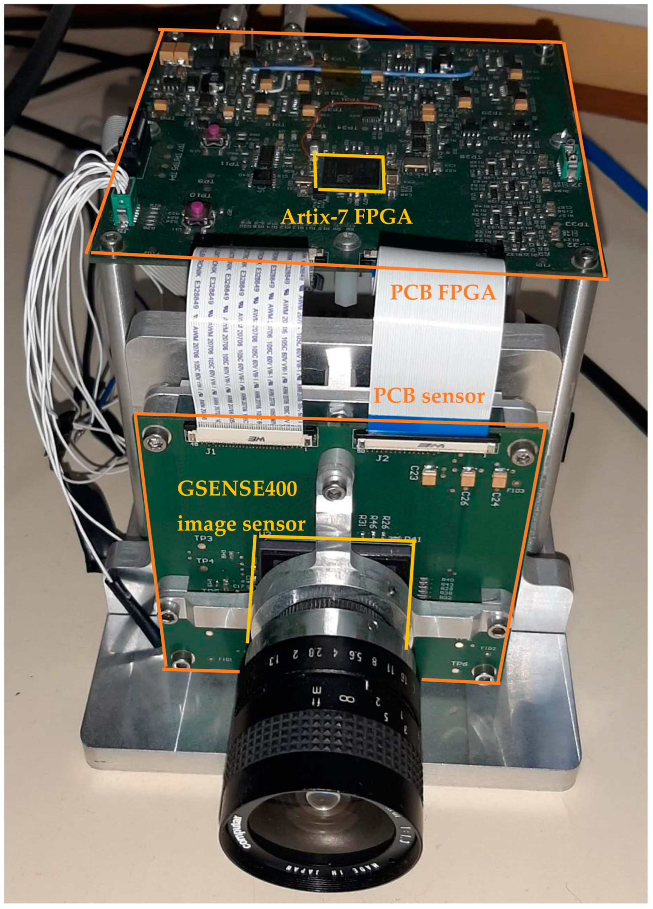
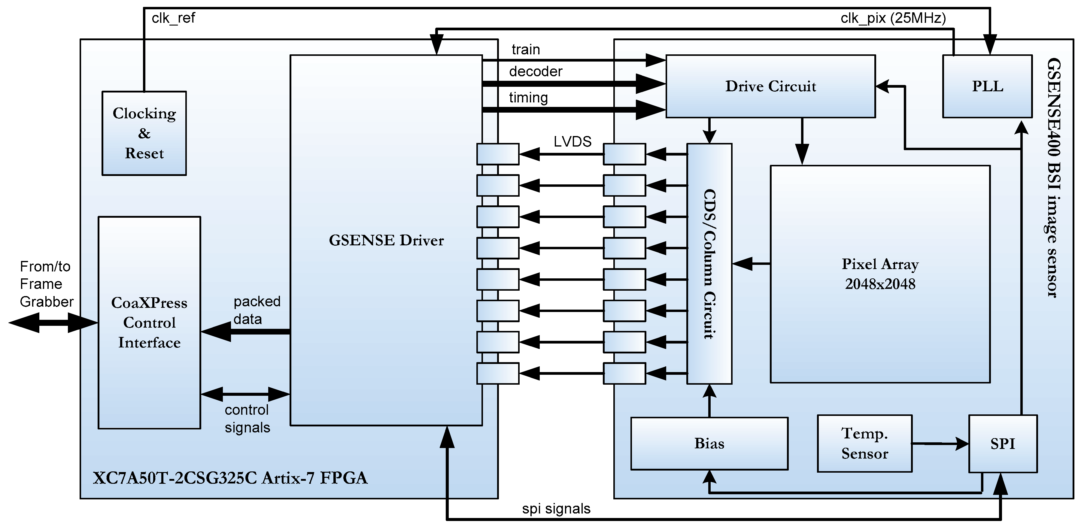
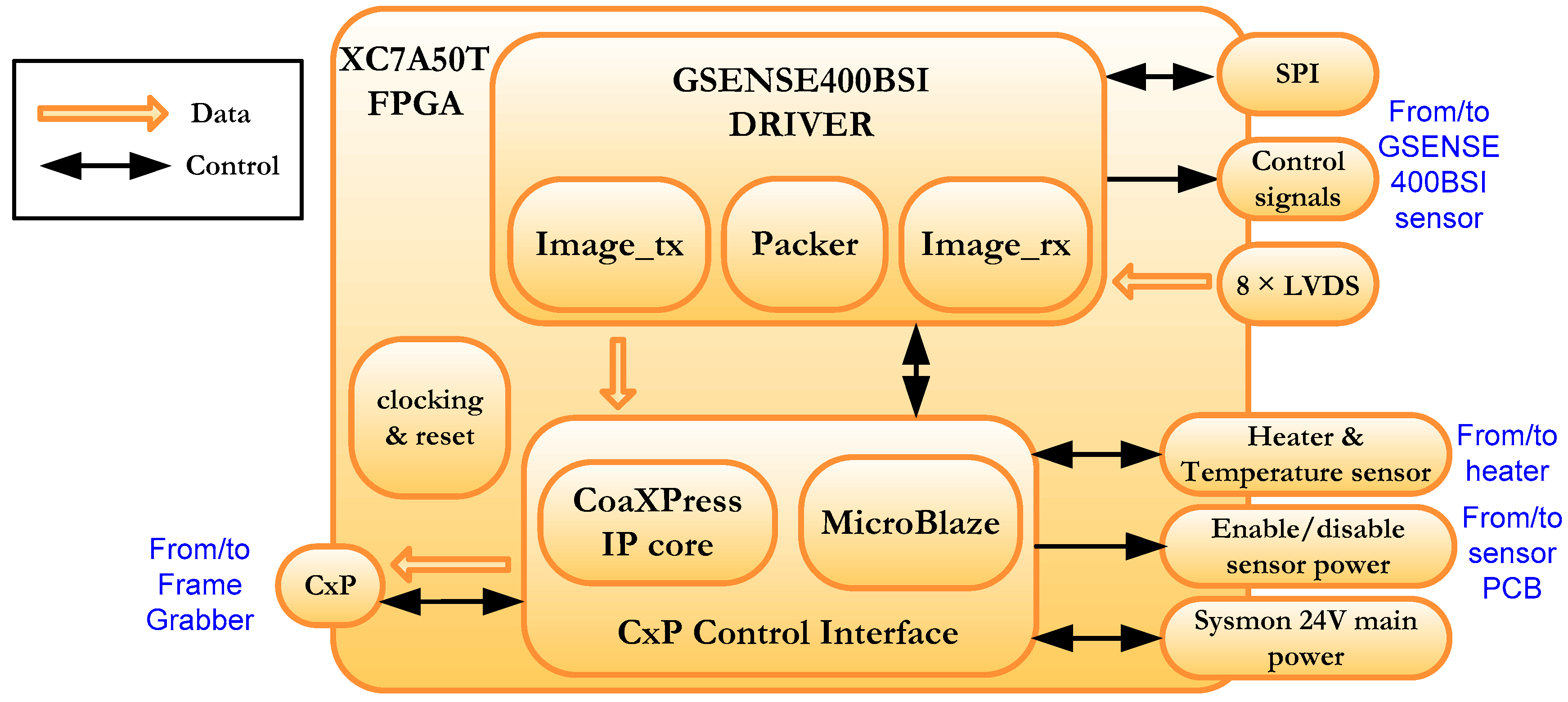
2. The TuMag Camera
3. TuMag Camera Firmware Overview
- Configuration of the sensor, through the SPI interface;
- Generation of the control signals necessary to grab images from the sensor, such as the 19 control signals and the row address signal (decoder and timing signals in Figure 1);
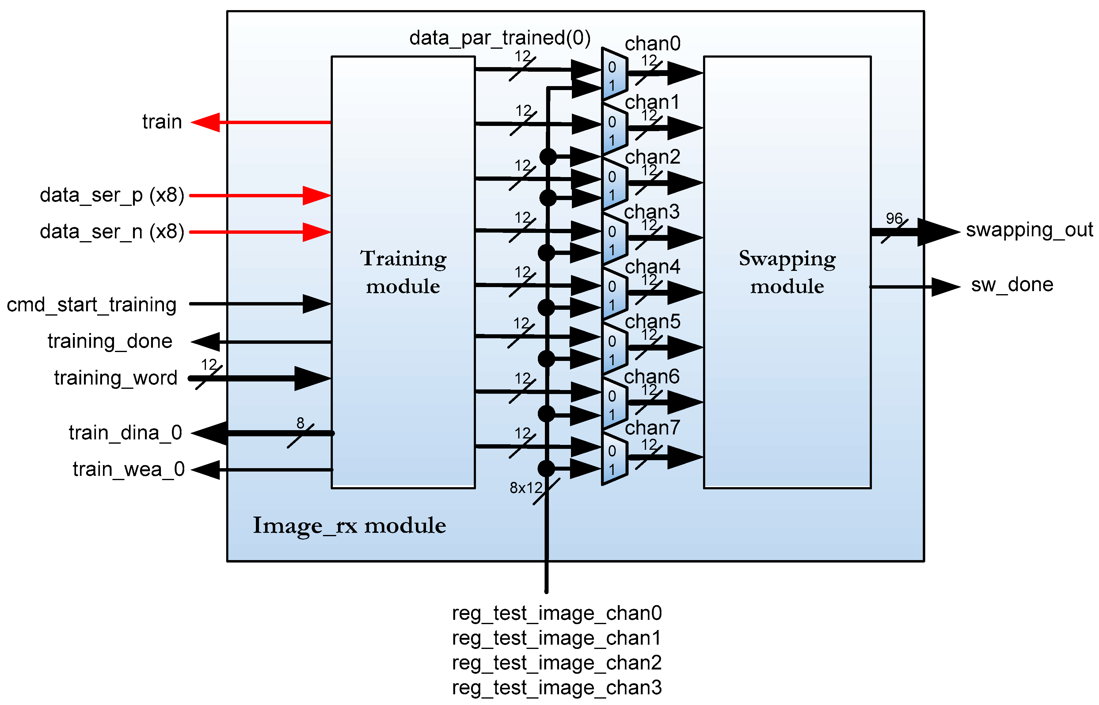
- Implementation of the image receiving interface (rx), based on 8 LVDS serial data channels from the camera that are converted to 8–12-bit parallel channels;
- Channels calibration task;
- Generation of the signals to arrange the received image;
- Image ordering and packing;
- Implementation of the image transmitting interface (tx) to CxP Control Interface.
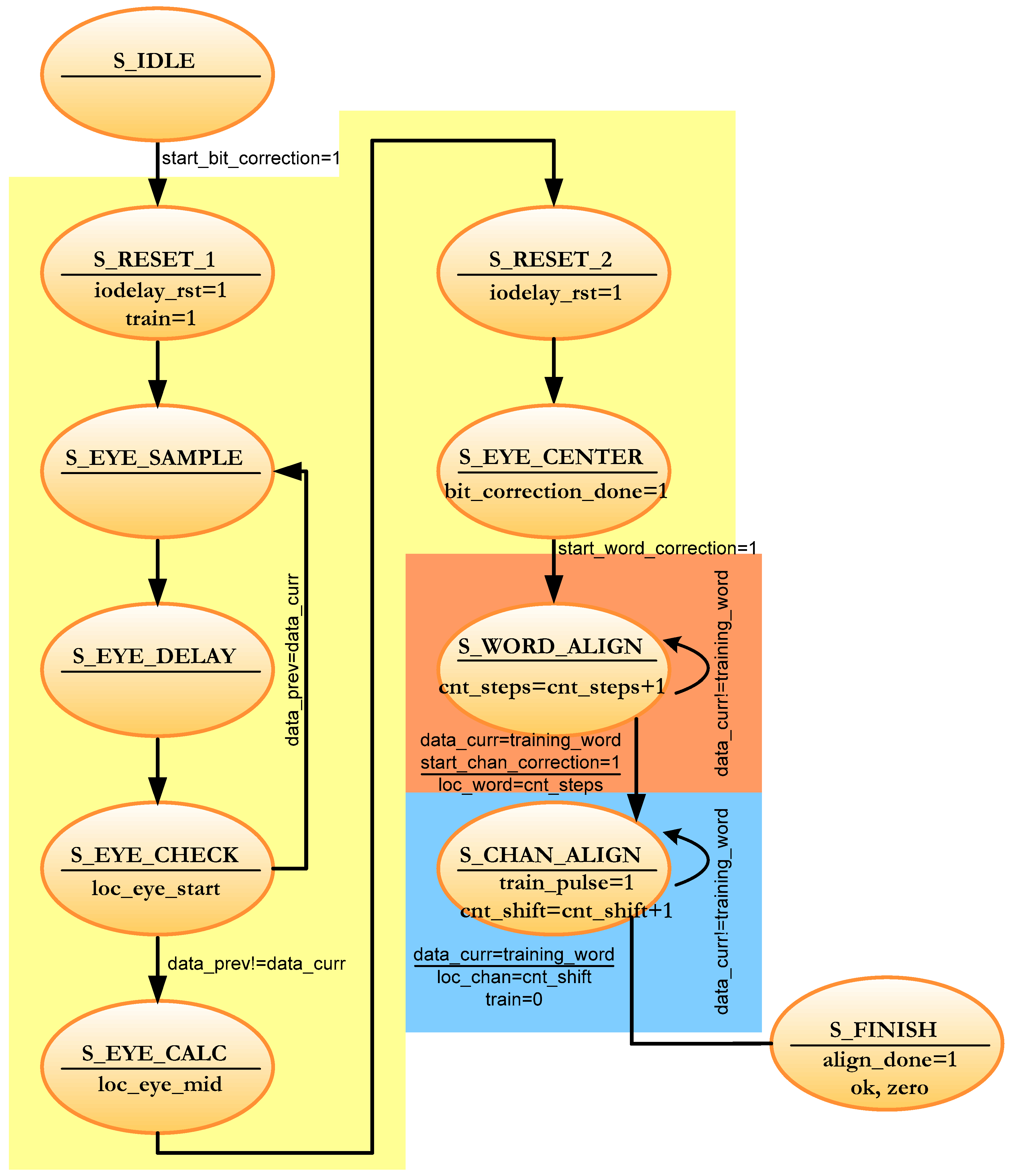
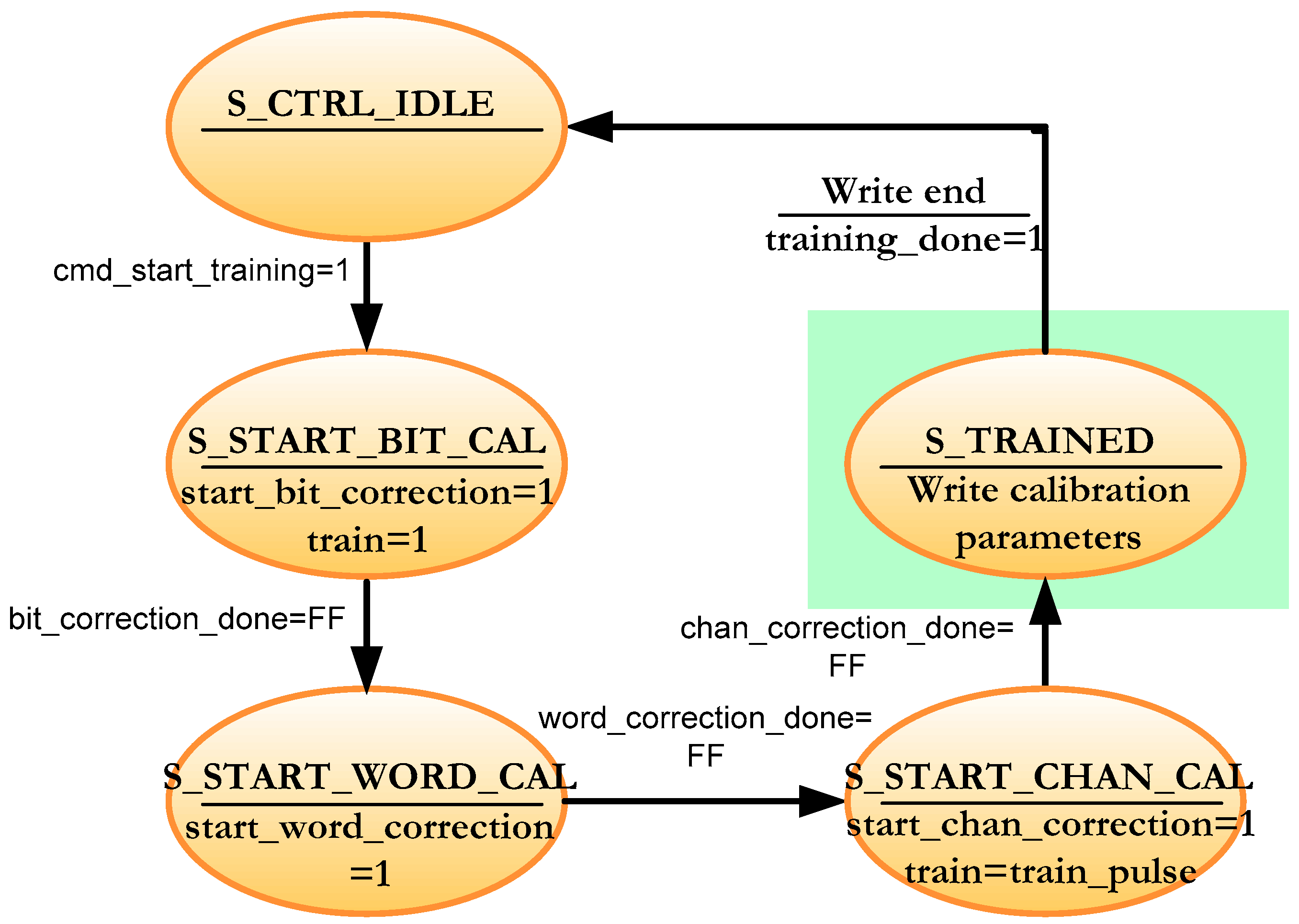
4. Channel Calibration
4.1. Migration of the Calibration Algorithm to Artix-7 FPGA
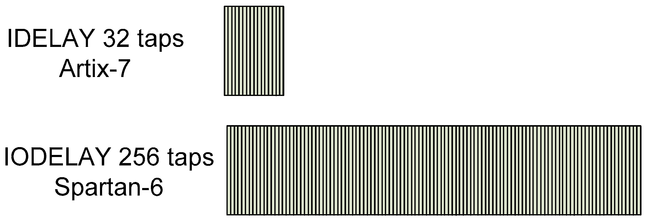
- Migration from Spartan-6 components to Artix-7 ad hoc components: substitution of IODELAY by IDELAY2, substitution of IDDR2 by IDDR. The 7-series devices have dedicated registers in the ILOGIC blocks to implement input double-data-rate (DDR) registers. This component is similar to the IDDR2 component of the Spartan-6 FPGA and direct replacement is possible [46,48]. However, the IDELAYE2 component of the Artix-7 FPGA differs greatly from its equivalent component of the Spartan-6 and direct replacement is not possible. The 6-series IODELAY component has a 256 tap-delay but the 7-series IDELAY2 has only 32 tap-delay [49]. Figure 9 depicts a comparison between both components;
- This time, the data capture mechanism is dependent on the IODELAY2 component instead IDELAY. The 6-series IODELAY component has a 256 tap-delay but the 7-series IDELAY2 has only a 32 tap-delay of nominally 78 ps and the minimum capture frequency = 78 × 31 = 2418 ps = 415 Mb/s. The frequency of the design is lower (300 Mb/s) and it could result in no edges at all being found. So, the previous algorithm using Spartan-6 FPGA has been modified to consider this situation;
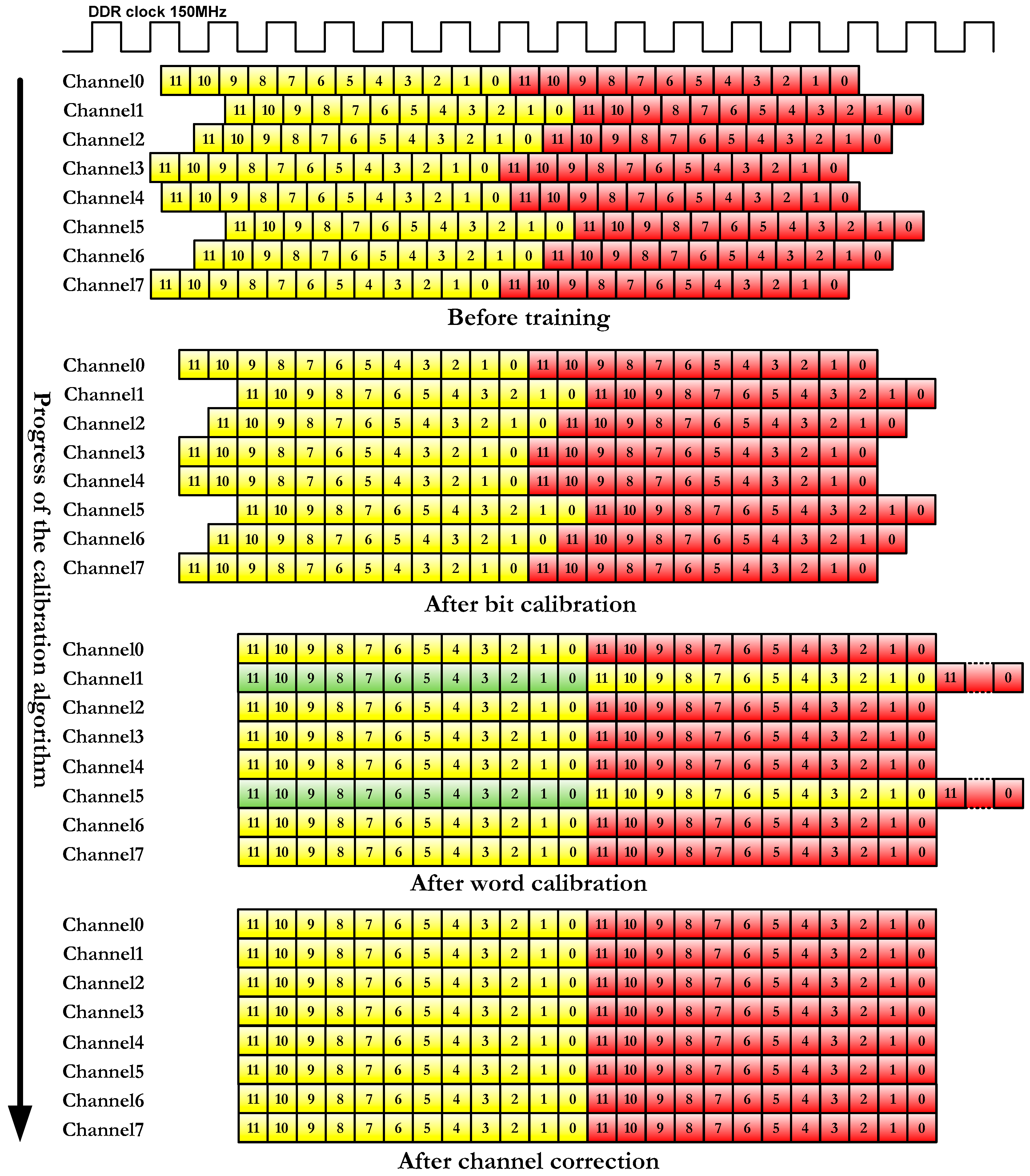
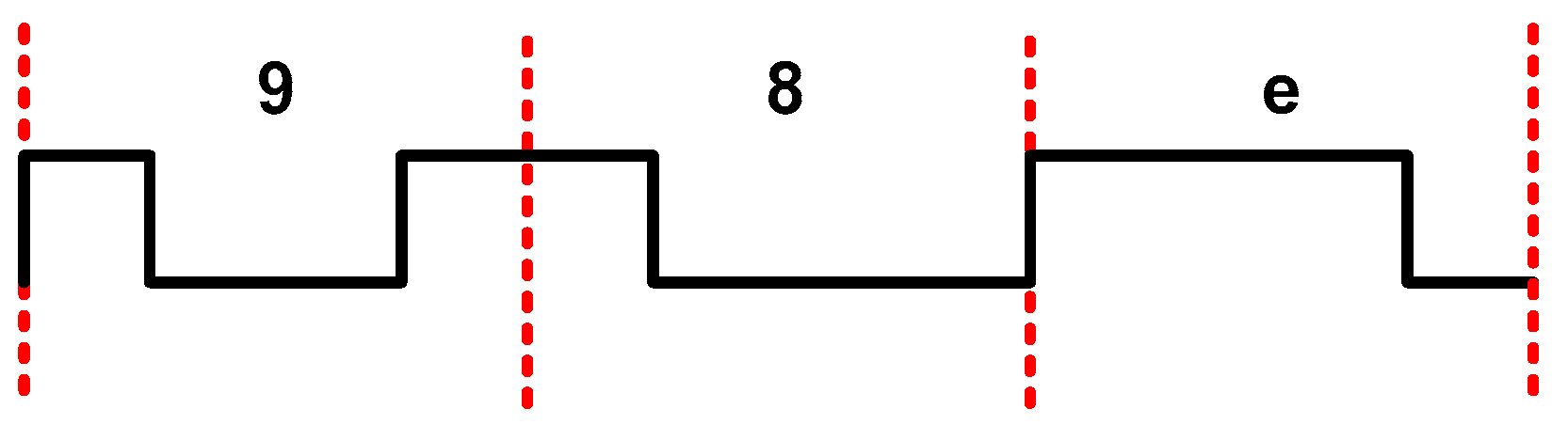
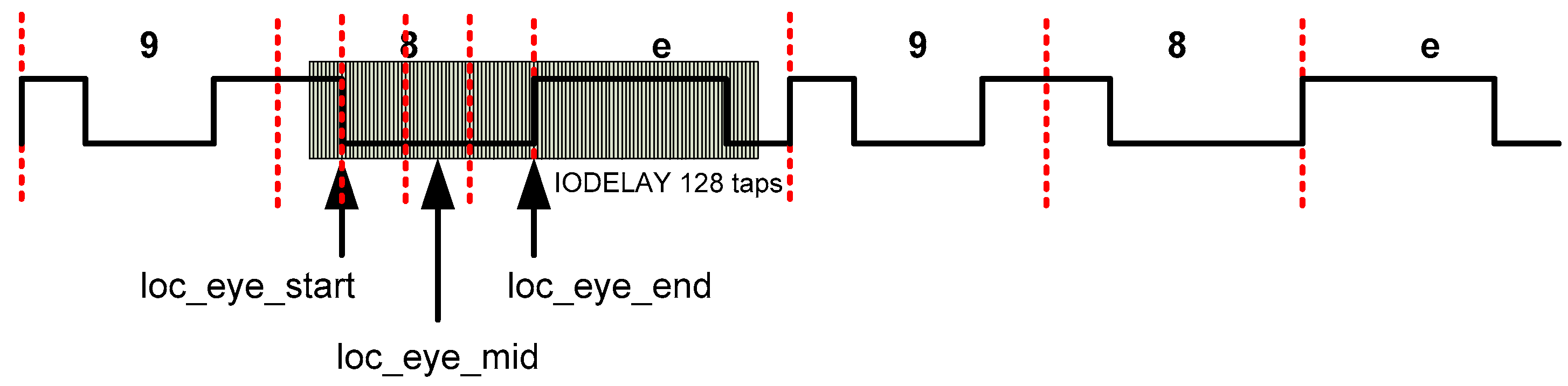
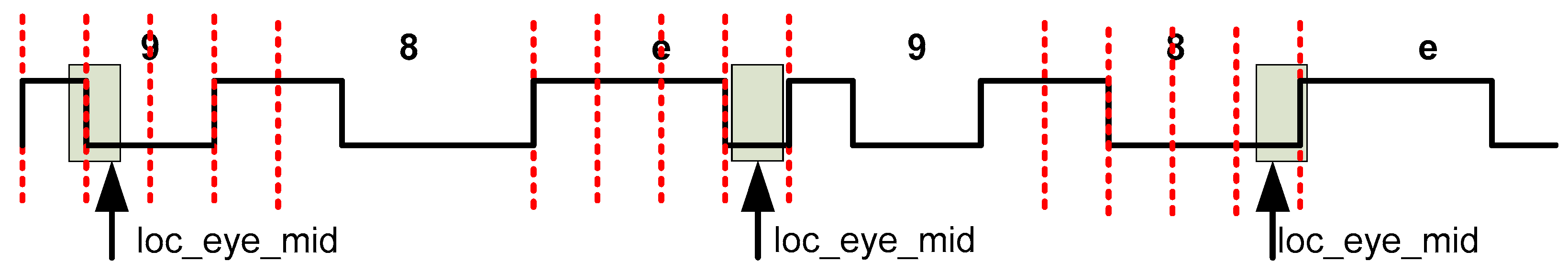
- The bit calibration for Spartan-6 searches 2 edges but the modification for Artix-7 FPGA searches only one edge. If an edge is found in the delay line, then the final delay is statically set to be this value, ±16 taps. If no edge is found, the delay line is set to be 16 taps. In either case, the delay is set to be at least 16 taps away from the edge of the eye, which is acceptable at these lower bit rates [41]. Figure 10 depicts the 3 possible situations in the edge detection mechanism. At left, the edge is detected with taps less than 16 (for example 3), so 16 is added (set to sample a number of taps equal to 19). In the center, no edge is detected, so sampling is set at 16 taps. On the right, the edge is detected with a tap greater than 16 (for example, 20), so 16 is subtracted (sampling with 4 taps).
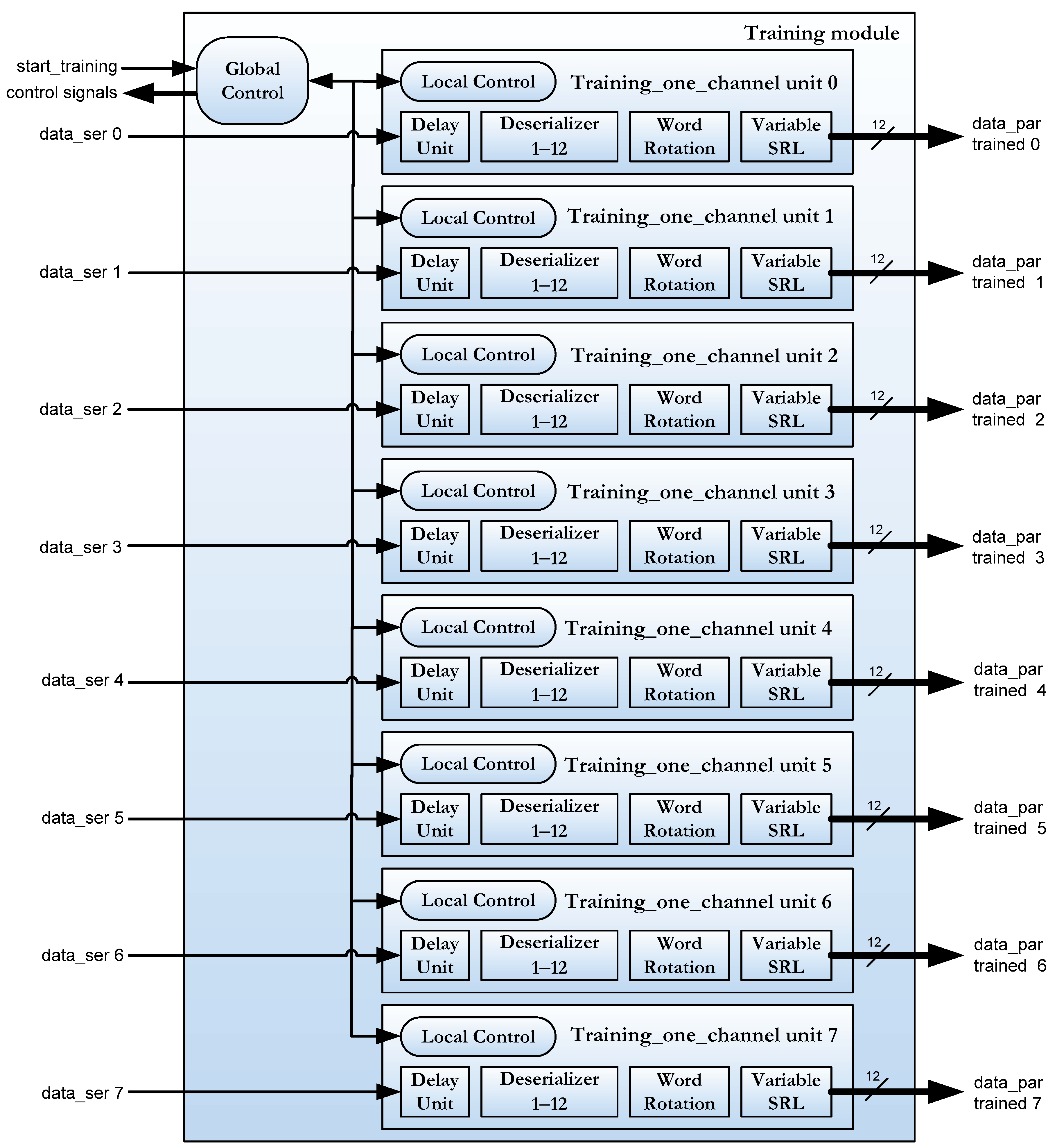
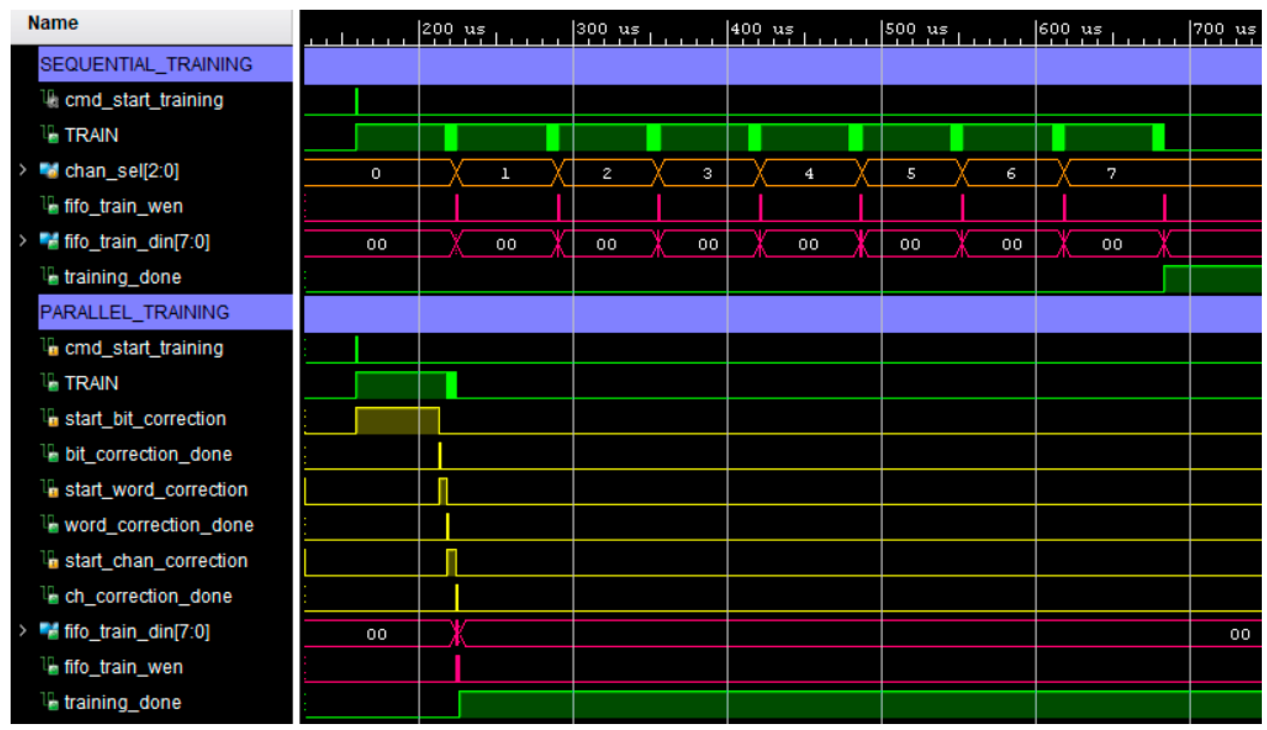
4.2. FPGA Concurrent Channel Calibration
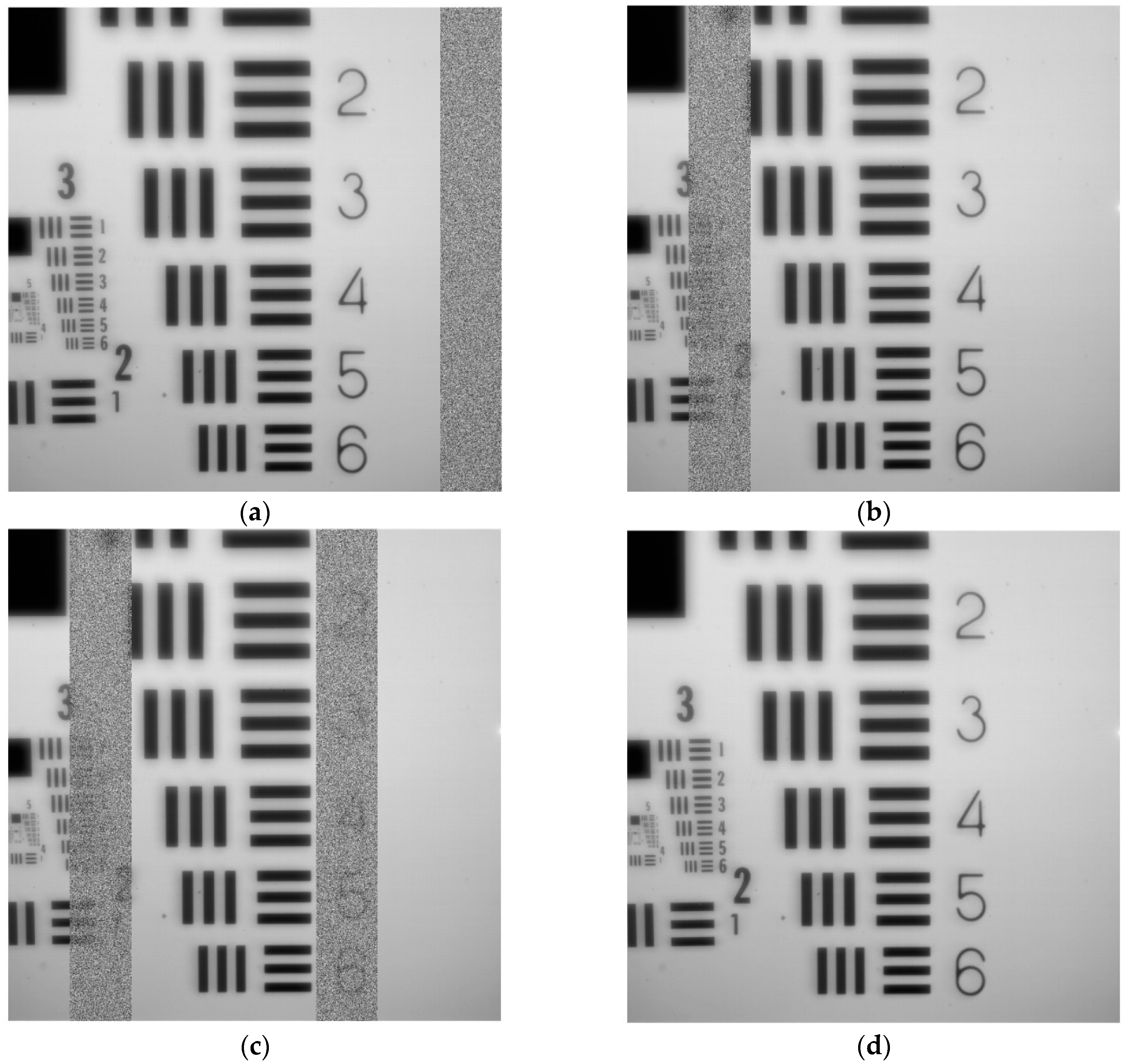
5. Results
6. Conclusions
Author Contributions
Funding
Institutional Review Board Statement
Informed Consent Statement
Data Availability Statement
Conflicts of Interest
References
- Quintero Noda, C.; Katsukawa, Y.; Shimizu, T.; Kubo, M.; Oba, T.; Ichimoto, K. Sunrise-3: Science target and mission capabilities for understanding the solar atmosphere. In Proceedings of the 19th Space Science Symposium, Sagamihara, Japan, 9 January 2019. [Google Scholar]
- Gandorfer, A.; Solanki, S.K.; Woch, J.; Pillet, V.M.; Herrero, A.A.; Appourchaux, T. The Solar Orbiter Mission and its Polarimetric and Helioseismic Imager (SO/PHI). J. Phys. Conf. Ser. 2011, 271, 8. [Google Scholar] [CrossRef]
- Pillet, V.M.; Del Toro Iniesta, J.C.; Álvarez-Herrero, A.; Domingo, V.; Bonet, J.A.; Fernández, L.G.; Jiménez, A.L.; Pastor, C.; Blesa, J.G.; Mellado, P.; et al. The Imaging Magnetograph eXperiment (IMaX) for the Sunrise Balloon-Borne Observatory. Sol. Phys. 2011, 268, 57–102. [Google Scholar]
- Barthol, P. The Sunrise Balloon-Borne Stratospheric Solar Observatory, 1st ed.; Springer: New York, NY, USA, 2011; pp. 1–123. [Google Scholar]
- Barthol, P.; Gandorfer, A.; Solanki, S.K.; Schüssler, M.; Chares, B.; Curdt, W.; Deutsch, W.; Feller, A.; Germerott, D.; Grauf, B.; et al. The Sunrise Mission. Sol. Phys. 2011, 268, 1–34. [Google Scholar] [CrossRef] [Green Version]
- Solanki, S.K.; Barthol, P.; Danilovic, S.; Feller, A.; Gandorfer, A.; Hirzberger, J.; Riethmüller, T.L.; Schüssler, M.; Bonet, J.A.; Pillet, V.M.; et al. Sunrise: Instrument, Mission, Data, and First Results. Astrophys. J. Lett. 2010, 723, L127–L133. [Google Scholar] [CrossRef]
- Solanki, S.K.; Riethmüller, T.L.; Barthol, P.; Danilovic, S.; Deutsch, W.; Doerr, H.P.; Feller, A.; Gandorfer, A.; Germerott, D.; Gizon, L.; et al. The Second Flight of SUNRISE Balloon-borne Solar Observatory: Overview of Instrument Updates, the Flight, the Data, and First Results. Astrophys. J. Suppl. Ser. 2017, 229, 16. [Google Scholar] [CrossRef] [Green Version]
- Kaithakkal, A.J.; Riethmüller, T.L.; Solanki, S.K.; Lagg, A.; Barthol, P.; Gandorfer, A.; Gizon, L.; Hirzberger, J.; Rodríguez, J.B.; Iniesta, J.D.T.; et al. Moving Magnetic Features Around a Pore. Astrophys. J. Suppl. Ser. 2017, 229, 13. [Google Scholar] [CrossRef] [Green Version]
- Centeno, R.; Rodríguez, J.B.; Iniesta, J.D.T.; Solanki, S.K.; Barthol, P.; Gandorfer, A.; Gizon, L.; Hirzberger, J.; Riethmüller, T.L.; van Noort, M.; et al. A Tale of Two Emergences: SUNRISE II Observations of Emergence Sites in a Solar Active Region. Astrophys. J. Suppl. Ser. 2017, 229, 3. [Google Scholar] [CrossRef] [Green Version]
- Requerey, I.S.; Iniesta, J.C.D.T.; Rubio, L.R.B.; Bonet, J.A.; Pillet, V.M.; Solanki, S.K.; Schmidt, W. The History of a Quiet-Sun Magnetic Element Revealed by IMaX/SUNRISE. Astrophys. J. Suppl. Ser. 2014, 789, 12. [Google Scholar] [CrossRef] [Green Version]
- Requerey, I.S.; Cobo, B.R.; Iniesta, J.D.T.; Suárez, D.O.; Rodríguez, J.B.; Solanki, S.K.; Barthol, P.; Gandorfer, A.; Gizon, L.; Hirzberger, J.; et al. Spectropolarimetric Evidence for a Siphon Flow along an Emerging Magnetic Flux Tube. Astrophys. J. Suppl. Ser. 2017, 229, 5. [Google Scholar] [CrossRef] [Green Version]
- Berkefeld, T.; Schmidt, W.; Soltau, D.; Bell, A.; Doerr, H.P.; Feger, B.; Friedlein, R.; Gerber, K.; Heidecke, F.; Kentischer, T.; et al. The Wave-Front Correction System for the Sunrise Balloon-Borne Solar Observatory. Sol. Phys. 2011, 268, 103–123. [Google Scholar] [CrossRef] [Green Version]
- Riethmüller, T.L.; Solanki, S.K.; Barthol, P.; Gandorfer, A.; Gizon, L.; Hirzberger, J.; Van Noort, M.; Rodríguez, J.B.; Iniesta, J.D.T.; Suárez, D.O.; et al. A New MHD-assisted Stokes Inversion Technique. Astrophys. J. Suppl. Ser. 2017, 229, 14. [Google Scholar] [CrossRef] [Green Version]
- Orozco Suárez, D.; Bellot Rubio, L.R.; del Toro Iniesta, J.C.; Tsuneta, S.; Lites, B.W.; Ichimoto, K.; Katsukawa, Y.; Nagata, S.; Shimizu, T.; Shine, R.A.; et al. Quiet-Sun Internetwork Magnetic Fields from the Inversion of Hinode Measurements. Astrophys. J. 2007, 670, L61–L64. [Google Scholar] [CrossRef] [Green Version]
- Castelló, E.M.; Valido, M.R.; Expósito, D.H.; Cobo, B.R.; Balaguer, M.; Suárez, D.O.; Jiménez, A.L. IMAX+ camera prototype as a teaching resource for calibration and image processing using FPGA devices. In Proceedings of the 2020 XIV Technologies Applied to Electronics Teaching Conference (TAEE), Porto, Portugal, 8–10 July 2020. [Google Scholar]
- Katsukawa, Y.; del Toro Iniesta, J.C.; Solanki, S.K.; Kubo, M.; Hara, H.; Shimizu, T.; Oba, T.; Kawabata, Y.; Tsuzuki, T.; Uraguchi, F.; et al. Sunrise Chromospheric Infrared SpectroPolarimeter (SCIP) for sunrise III: System design and capability, in Ground-based and Airborne Instrumentation for Astronomy VIII. In Proceedings of the SPIE Astronomical Telescopes + Instrumentation, Online, 14–18 December 2020. [Google Scholar] [CrossRef]
- Feller, A.; Gandorfer, A.; Iglesias, F.A.; Lagg, A.; Riethmüller, T.L.; Solanki, S.K.; Katsukawa, Y.; Kubo, M. The SUNRISE UV Spectropolarimeter and Imager for SUNRISE III. In Proceedings of the SPIE 11447, Ground-Based and Airborne Instrumentation for Astronomy VIII, Online, 14–18 December 2020. [Google Scholar] [CrossRef]
- Toshihiro, T.; Katsukawa, Y.; Uraguchi, F.; Hara, H.; Kubo, M.; Nodomi, Y.; Suematsu, Y.; Kawabata, Y.; Shimizu, T.; Gandorfer, A.; et al. Sunrise Chromospheric Infrared spectroPolarimeter (SCIP) for SUNRISE III: Optical design and performance. In Proceedings of the SPIE 11447, Ground-Based and Airborne Instrumentation for Astronomy VIII, Online, 14–18 December 2020. [Google Scholar] [CrossRef]
- Kubo, M.; Shimizu, T.; Katsukawa, Y.; Kawabata, Y.; Anan, T.; Ichimoto, K.; Shinoda, K.; Tamura, T.; Nodomi, Y.; Nakayama, S.; et al. Sunrise Chromospheric Infrared spectroPolarimeter (SCIP) for SUNRISE III: Polarization Modulation unit. In Proceedings of the SPIE 11447, Ground-Based and Airborne Instrumentation for Astronomy VIII, Online, 14–18 December 2020. [Google Scholar] [CrossRef]
- Uraguchi, F.; Tsuzuki, T.; Katsukawa, Y.; Hara, H.; Iwamura, S.; Kubo, M.; Nodomi, Y.; Suematsu, Y.; Kawabata, Y.; Shimizu, T. Sunrise Chromospheric Infrared spectroPolarimeter (SCIP) for SUNRISE III: Opto-mechanical analysis and design. In Proceedings of the SPIE 11447, Ground-Based and Airborne Instrumentation for Astronomy VIII, Online, 14–18 December 2020. [Google Scholar] [CrossRef]
- Gpixel. GSENSE400 4 Megapixels Scientific CMOS Image Sensor. Datasheet V1.5; Gpixel Inc.: Changchum, China, 2017. [Google Scholar]
- Xilinx Inc. 7 Series FPGAs Data Sheet: Overview. Product Specification. DS180 (v2.6.1). 2020. Available online: https://www.xilinx.com/support/documentation/data_sheets/ds180_7Series_Overview.pdf (accessed on 22 November 2021).
- Tang, X.; Liu, G.; Qian, Y.; Cheng, H.; Qiao, K. A Handheld High-Resolution Low-Light Camera. In Proceedings of the SPIE 11023, Fifth Symposium on Novel Optoelectronic Detection Technology and Application, Xi’an, China, 12 March 2019; Volume 110230X. [Google Scholar] [CrossRef]
- Xilinx Inc. Spartan-6 Family Overview. Product Specification. DS160 (v2.0). 2011. Available online: https://www.xilinx.com/support/documentation/data_sheets/ds160.pdf (accessed on 22 November 2021).
- Xilinx Inc. Artix-7 FPGAs Data Sheet: DC and AC Switching Characteristics. Product Specification. DS181 (v1.26). 2021. Available online: https://www.xilinx.com/support/documentation/data_sheets/ds181_Artix_7_Data_Sheet.pdf (accessed on 22 November 2021).
- Xilinx Inc. Spartan-6 Libraries Guide for HDL Designs. User Guide. UG615 (v14.7). 2013. Available online: https://www.xilinx.com/support/documentation/sw_manuals/xilinx14_7/spartan6_hdl.pdf (accessed on 22 November 2021).
- Xilinx Inc. Xilinx 7 Series FPGA and Zynq-7000 All Programmable SoC Libraries Guide for HDL Designs. User Guide. UG768 (v14.7). 2013. Available online: https://www.xilinx.com/support/documentation/sw_manuals/xilinx14_7/7series_hdl.pdf (accessed on 22 November 2021).
- Heng, Z.; Qing-jun, M.; Shu-rong, W. High speed CMOS imaging electronics system for ultraviolet remote sensing instrument. Opt. Precis. Eng. 2018, 26, 471–479. [Google Scholar] [CrossRef]
- Ma, C.; Liu, Y.; Li, J.; Zhou, Q.; Chang, Y.; Wang, X. A 4MP high-dynamic-range, low-noise CMOS image sensor. In Proceedings of the SPIE 9403, Image Sensors and Imaging Systems 2015, San Francisco, CA, USA, 13 March 2015; Volume 940305. [Google Scholar] [CrossRef]
- Wang, F.; Dai, M.; Sun, Q.; Ai, L. Design and implementation of CMOS-based low-light level night-vision imaging system. In Proceedings of the SPIE 11763, Seventh Symposium on Novel Photoelectronic Detection Technology and Applications, San Francisco, CA, USA, 12 March 2021; Volume 117635O. [Google Scholar] [CrossRef]
- Magdaleno, E.; Rodríguez, M.; Rodríguez-Ramos, J.M. An Efficient Pipeline Wavefront Phase Recovery for the CAFADIS Camera for Extremely Large Telescopes. Sensors 2010, 10, 1–15. [Google Scholar] [CrossRef] [PubMed]
- Magdaleno, E.; Lüke, J.P.; Rodríguez, M.; Rodríguez-Ramos, J.M. Design of Belief Propagation Based on FPGA for the Multistereo CAFADIS Camera. Sensors 2010, 10, 9194–9210. [Google Scholar] [CrossRef] [PubMed] [Green Version]
- Pérez, J.; Magdaleno, E.; Pérez, F.; Rodríguez, M.; Hernández, D.; Corrales, J. Super-Resolution in Plenoptic Cameras Using FPGAs. Sensors 2014, 14, 8669–8685. [Google Scholar] [CrossRef] [PubMed] [Green Version]
- Rodríguez, M.; Magdaleno, E.; Pérez, F.; García, C. Automated Software Acceleration in Programmable Logic for an Efficient NFFT Algorithm Implementation: A Case Study. Sensors 2017, 17, 694. [Google Scholar] [CrossRef] [Green Version]
- Alvear, A.; Finger, R.; Fuentes, R.; Sapunar, R.; Geelen, T.; Curotto, F.; Rodríguez, R.; Monasterio, D.; Reyes, N.; Mena, P.; et al. FPGA-based digital signal processing for the next generation radio astronomy instruments: Ultra-pure sideband separation and polarization detection, in Millimeter, Submillimeter, and Far-Infrared Detectors and Instrumentation for Astronomy VIII. In Proceedings of the SPIE, Edinburgh, UK, 26 June–1 July 2016; Volume 9914. [Google Scholar] [CrossRef]
- Schwanke, U.; Shayduk, M.; Sulanke, K.-H.; Vorobiov, S.; Wischnewski, R. A Versatile Digital Camera Trigger for Telescopes in the Cherenkov Telescope Array. In Nuclear Instruments and Methods in Physics Research Section A: Accelerators Spectrometers Detectors and Associated Equipment; Elsevier: Amsterdam, The Netherland, 2015; Volume 782, pp. 92–103. [Google Scholar] [CrossRef] [Green Version]
- Lecerf, A.; Ouellet, D.; Arias-Estrada, M. Computer vision camera with embedded FPGA processing. In Proceedings of the SPIE 3966, Machine Vision Applications in Industrial Inspection VIII, San Jose, CA, USA, 21 March 2000. [Google Scholar] [CrossRef]
- Heller, M.; Schioppa, E.; Jr Porcelli, A.; Pujadas, I.T.; Ziȩtara, K.; Della Volpe, D.; Montaruli, T.; Cadoux, F.; Favre, Y.; Aguilar, J.A.; et al. An innovative silicon photomultiplier digitizing camera for gamma-ray astronomy. Eur. Phys. J. C 2017, 77, 47. [Google Scholar] [CrossRef] [Green Version]
- Magdaleno, E.; Rodríguez, M.; Hernández, D.; Balaguer, M.; Ruiz-Cobo, B. FPGA implementation of Image Ordering and Packing for TuMag Camera. Electronics 2021, 10, 1706. [Google Scholar] [CrossRef]
- EASii IC. CoaxPress Device IP Specification. Hard Soft Interface Document. IC/130206; EASii IC SAS: Grenoble, France, 2017. [Google Scholar]
- Sawyer, N. LVDS Source Synchronous 7:1 Serialization and Deserialization Using Clock Multiplication. Xilinx XAPP585 (v.1.1.2). 2018. Available online: https://www.xilinx.com/support/documentation/application_notes/xapp585-lvds-source-synch-serdes-clock-multiplication.pdf (accessed on 2 December 2020).
- CoaxPress Host IP Specification. Hard Soft Interface Document. IC/130249; EASii IC SAS: Grenoble, France, 2017. [Google Scholar]
- Magdaleno, E.; Rodríguez, M. TuMag Camera Firmware design and implementation report. SR3-IMAXP-RP-SW730-001. Revision A. Release date 2020-08-01, La Laguna, Spain, September 2021.
- GenICam Standard. Generic Interface for Cameras. Version 2.1.1. Emva. Available online: https://www.emva.org/wp-content/uploads/GenICam_Standard_v2_1_1.pdf (accessed on 2 December 2020).
- MicroBlaze Processor Reference Guide. Xilinx UG984 (v2018.2). 2018. Available online: https://www.xilinx.com/support/documentation/sw_manuals/xilinx2018_2/ug984-vivado-microblaze-ref.pdf (accessed on 2 December 2020).
- Xilinx Inc. Spartan-6 FPGA SelectIO Resources. User Guide. UG381 (v1.7). 2015. Available online: https://www.xilinx.com/support/documentation/user_guides/ug381.pdf (accessed on 29 November 2021).
- Sawyer, N. Source-Synchronous Serialization and Deserialization (up to 1050 Mb/s). Xilinx XAPP1064 (v.1.2). 2013. Available online: https://www.xilinx.com/support/documentation/application_notes/xapp1064.pdf (accessed on 29 November 2021).
- Xilinx Inc. 7-Series FPGAs Migration. User Guide. UG429 (v1.2). 2018. Available online: https://www.xilinx.com/support/documentation/sw_manuals/ug429_7Series_Migration.pdf (accessed on 11 February 2022).
- Xilinx Inc. 7-Series FPGA SelectIO Resources. User Guide. UG471 (v1.10). 2018. Available online: https://www.xilinx.com/support/documentation/user_guides/ug471_7Series_SelectIO.pdf (accessed on 30 November 2021).
- Defossez, M.; Sawyer, N. LVDS Source Synchronous DDR Deserialization (up to 1600 Mb/s), XAPP1017 (v1.0). 2016. Available online: https://www.xilinx.com/support/documentation/application_notes/xapp1017-lvds-ddr-deserial.pdf (accessed on 14 February 2022).
- Xilinx Inc. SelectIO Interface Wizard v5.1. LogiCORE IP Product Guide PG070. 2016. Available online: https://www.xilinx.com/support/documentation/ip_documentation/selectio_wiz/v5_1/pg070-selectio-wiz.pdf (accessed on 14 February 2022).
- Liu, F.; Wang, L.; Yang, Y. A UHD MIPI CSI-2 image acquisition system based on FPGA. In Proceedings of the 40th Chinese Control Conference (CCC), IEEE Conference, Shanghai, China, 26–28 July 2021; pp. 5668–5673. [Google Scholar]
- Lee, P.H.; Lee, H.Y.; Kim, Y.W.; Hong, H.Y.; Jang, Y.C. A 10-Gbps receiver bridge chip with deserializer for FPGA-based frame grabber supporting MIPI CSI-2. IEEE Trans. Consum. Electron. 2017, 63, 209–2015. [Google Scholar] [CrossRef]


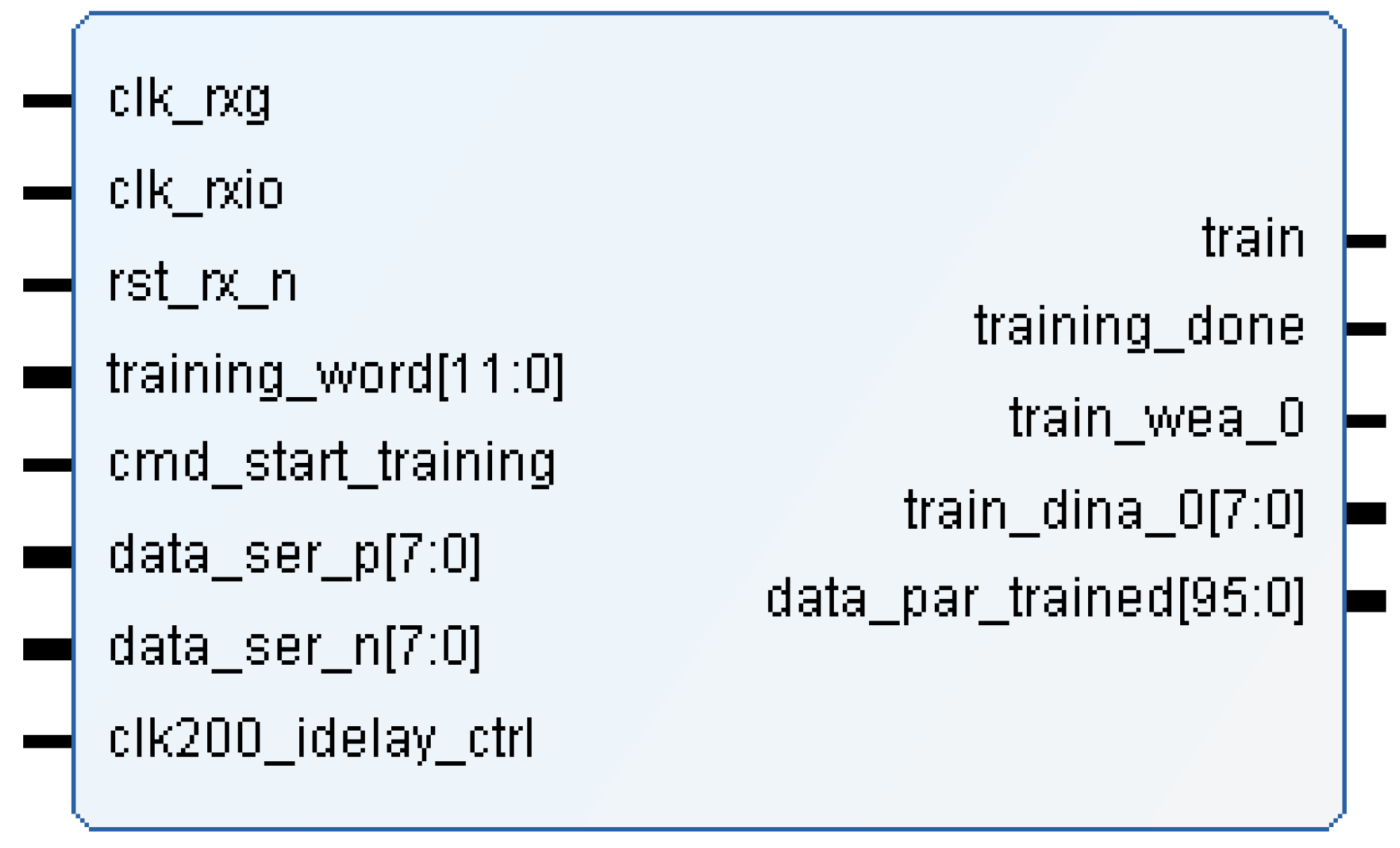
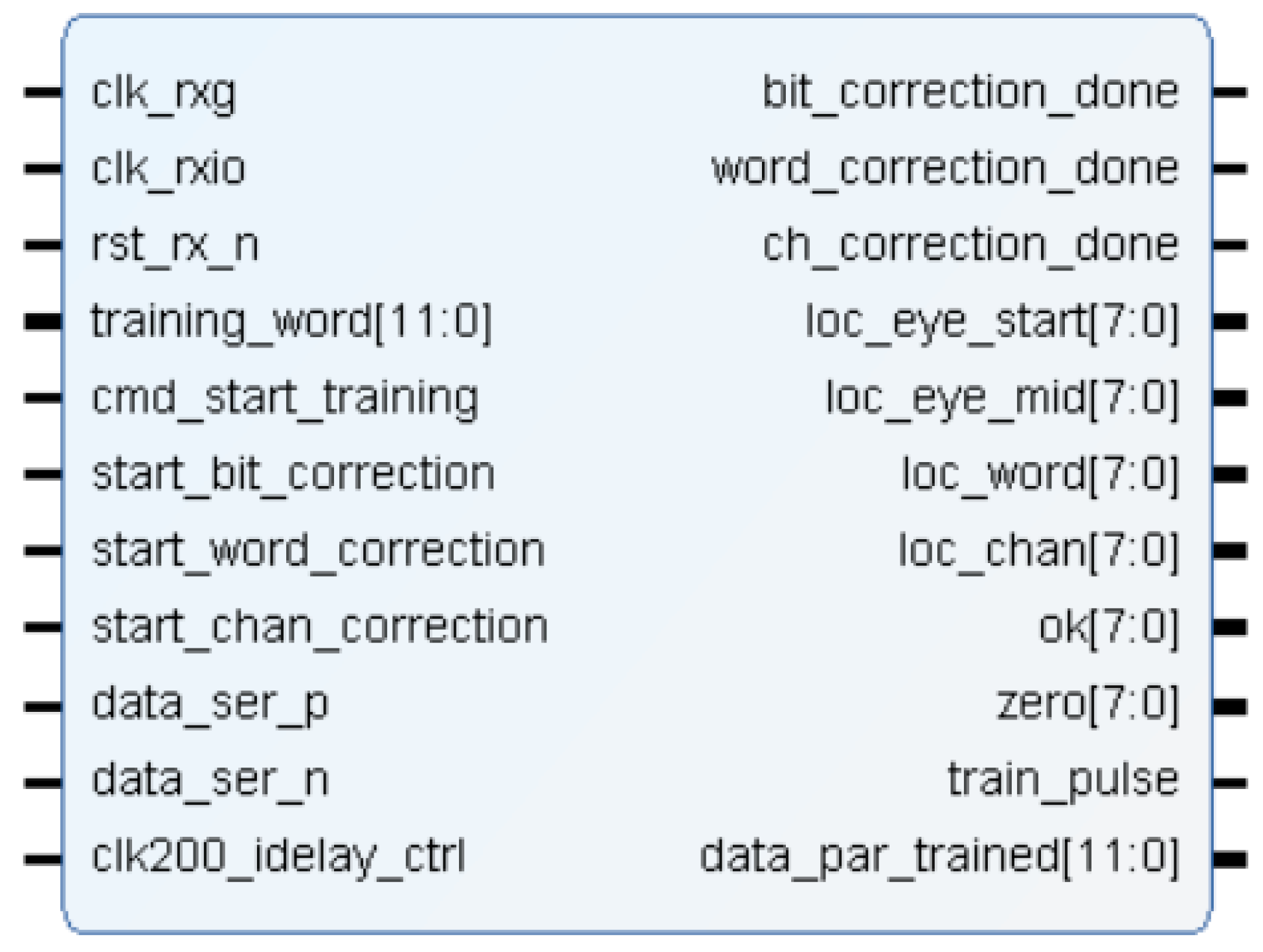
| Port | Description |
|---|---|
| clk_rxg | 25 MHz clock |
| clk_rxio | 150 MHz clock for sampling channels |
| rst_rx_n | low level reset |
| training_word | word used for calibration task by comparison |
| cmd_start_training | command for start training task |
| start_bit_correction | command to start bit correction |
| start_word_correction | command to start word correction |
| start_chan_correction | command to start channel correction |
| data_ser_p/n | 8-LVDS channels from the sensor |
| clk200_idelay_ctrl | 200 MHz reference clock |
| data_par_trained | parallelized and calibrated data (8 channels) |
| bit_correction_done | flag for the end of bit correction |
| word_correction_done | flag for the end of word correction |
| ch_correction_done | flag for the end of channel correction |
| loc_eye_start | Tap value for the edge detection |
| loc_eye_mid | Tap value for sampling |
| loc_word | Number of rotations |
| loc_chan | Number of shift register |
| ok | Calibration channel ok |
| zero | Zero value (for debug) |
| train_pulse | Train pulse order for channel calibration |
| data_par_trained | parallelized and calibrated data (1 channel) |
| Training Module | Time |
|---|---|
| Sequential calibration (Spartan-6) | 4122.58 μs |
| Adapted sequential calibration (Artix-7) | 524.88 μs |
| Concurrent calibration (Artix-7) | 60.44 μs |
| Available Resources | Sequential Calibration | Concurrent Calibration | |
|---|---|---|---|
| LUT | 32,600 | 303 (0.93%) | 1332 (4.09%) |
| Flip-flops | 65,200 | 463 (0.71%) | 973 (1.49%) |
| Liu et al. [52] | Our System | |
|---|---|---|
| System resolution | 3840 × 2160 | 2048 × 2048 |
| Maximum bandwidth per line | 891 Mbps | 300 Mbps |
| Deserialization ratio | 1:8 | 1:12 |
| Calibration implementation | ISERDES IP module | Structural HDL code |
| Hardware cost | Small | Small |
Publisher’s Note: MDPI stays neutral with regard to jurisdictional claims in published maps and institutional affiliations. |
© 2022 by the authors. Licensee MDPI, Basel, Switzerland. This article is an open access article distributed under the terms and conditions of the Creative Commons Attribution (CC BY) license (https://creativecommons.org/licenses/by/4.0/).
Share and Cite
Magdaleno, E.; Rodríguez Valido, M.; Hernández, D.; Balaguer, M.; Ruiz Cobo, B.; Orozco Suárez, D.; Álvarez García, D.; González, A.M. Enhanced Channel Calibration for the Image Sensor of the TuMag Instrument. Sensors 2022, 22, 2078. https://doi.org/10.3390/s22062078
Magdaleno E, Rodríguez Valido M, Hernández D, Balaguer M, Ruiz Cobo B, Orozco Suárez D, Álvarez García D, González AM. Enhanced Channel Calibration for the Image Sensor of the TuMag Instrument. Sensors. 2022; 22(6):2078. https://doi.org/10.3390/s22062078
Chicago/Turabian StyleMagdaleno, Eduardo, Manuel Rodríguez Valido, David Hernández, María Balaguer, Basilio Ruiz Cobo, David Orozco Suárez, Daniel Álvarez García, and Argelio Mauro González. 2022. "Enhanced Channel Calibration for the Image Sensor of the TuMag Instrument" Sensors 22, no. 6: 2078. https://doi.org/10.3390/s22062078
APA StyleMagdaleno, E., Rodríguez Valido, M., Hernández, D., Balaguer, M., Ruiz Cobo, B., Orozco Suárez, D., Álvarez García, D., & González, A. M. (2022). Enhanced Channel Calibration for the Image Sensor of the TuMag Instrument. Sensors, 22(6), 2078. https://doi.org/10.3390/s22062078