
Triboelectric Nanogenerators as Active Tactile Stimulators for Multifunctional Sensing and Artificial Synapses


Abstract
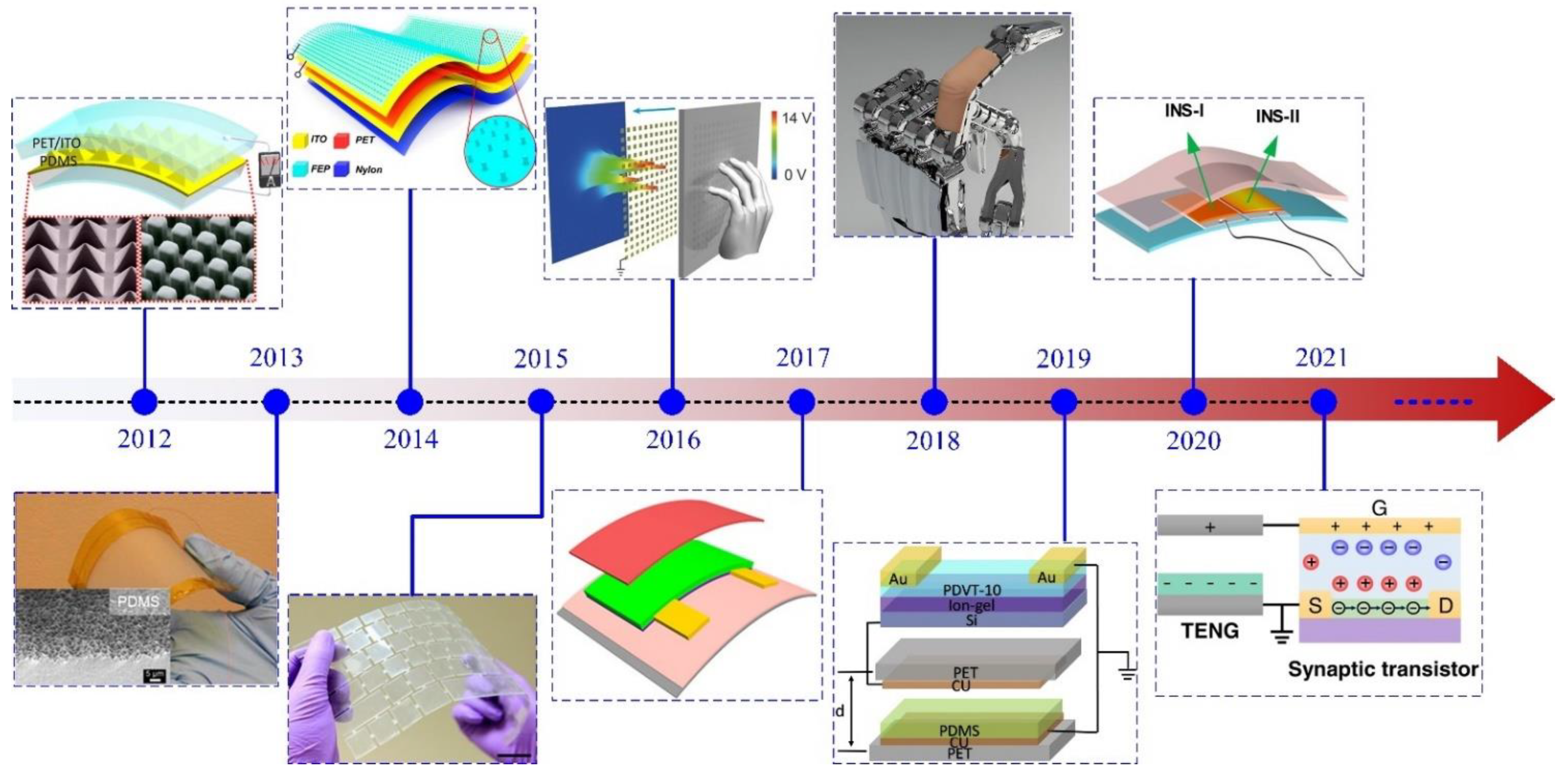
:1. Introduction
2. TENGs as Tactile Stimulators for Multifunctional Sensing
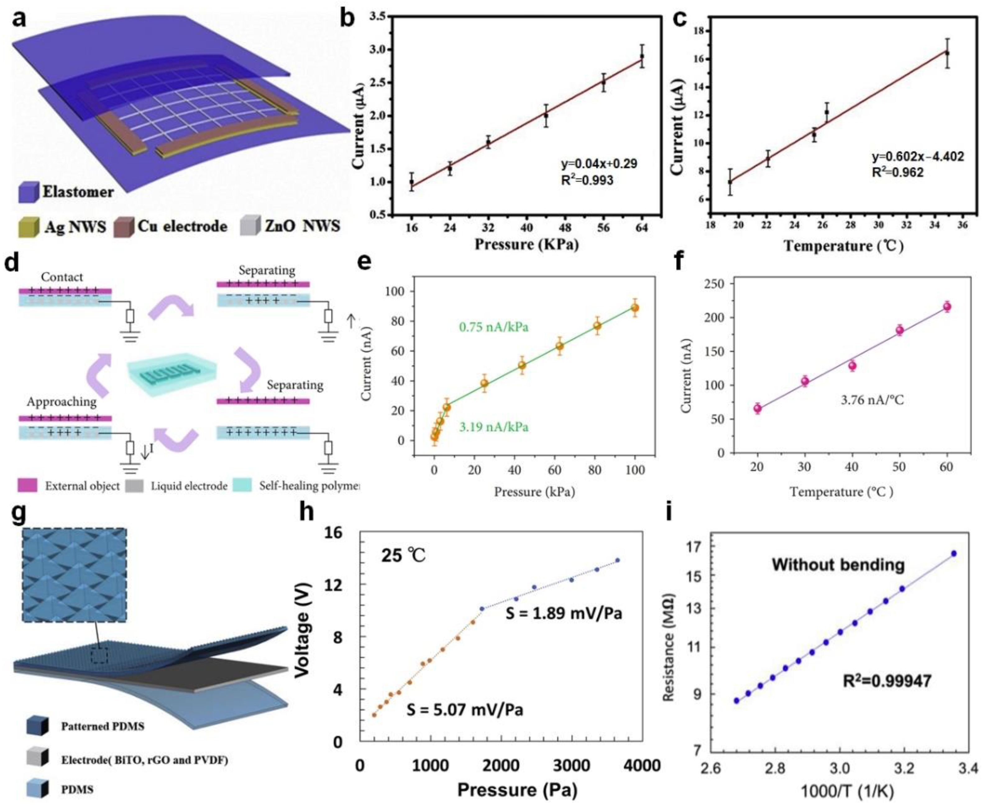
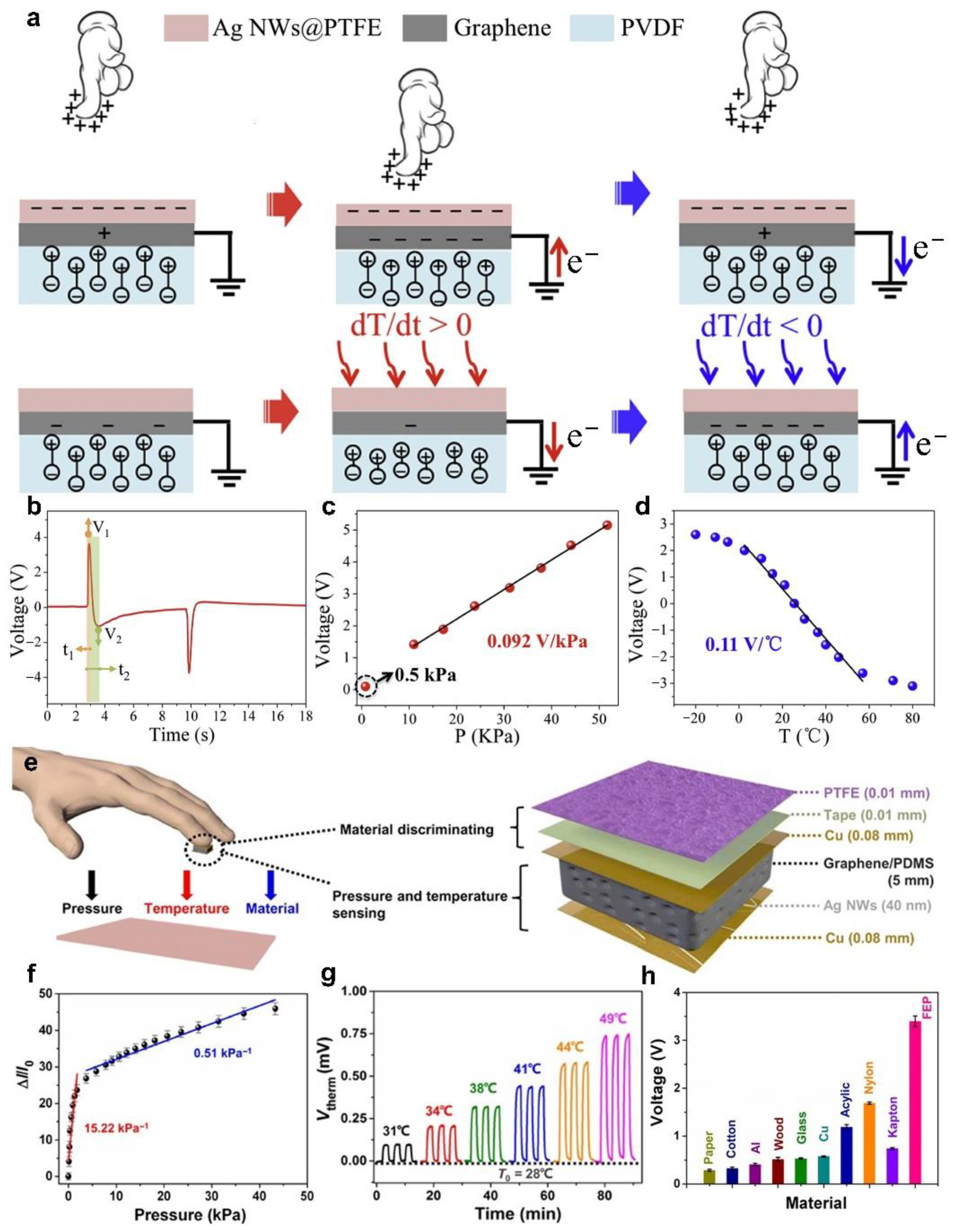
2.1. Pressure and Temperature Sensing
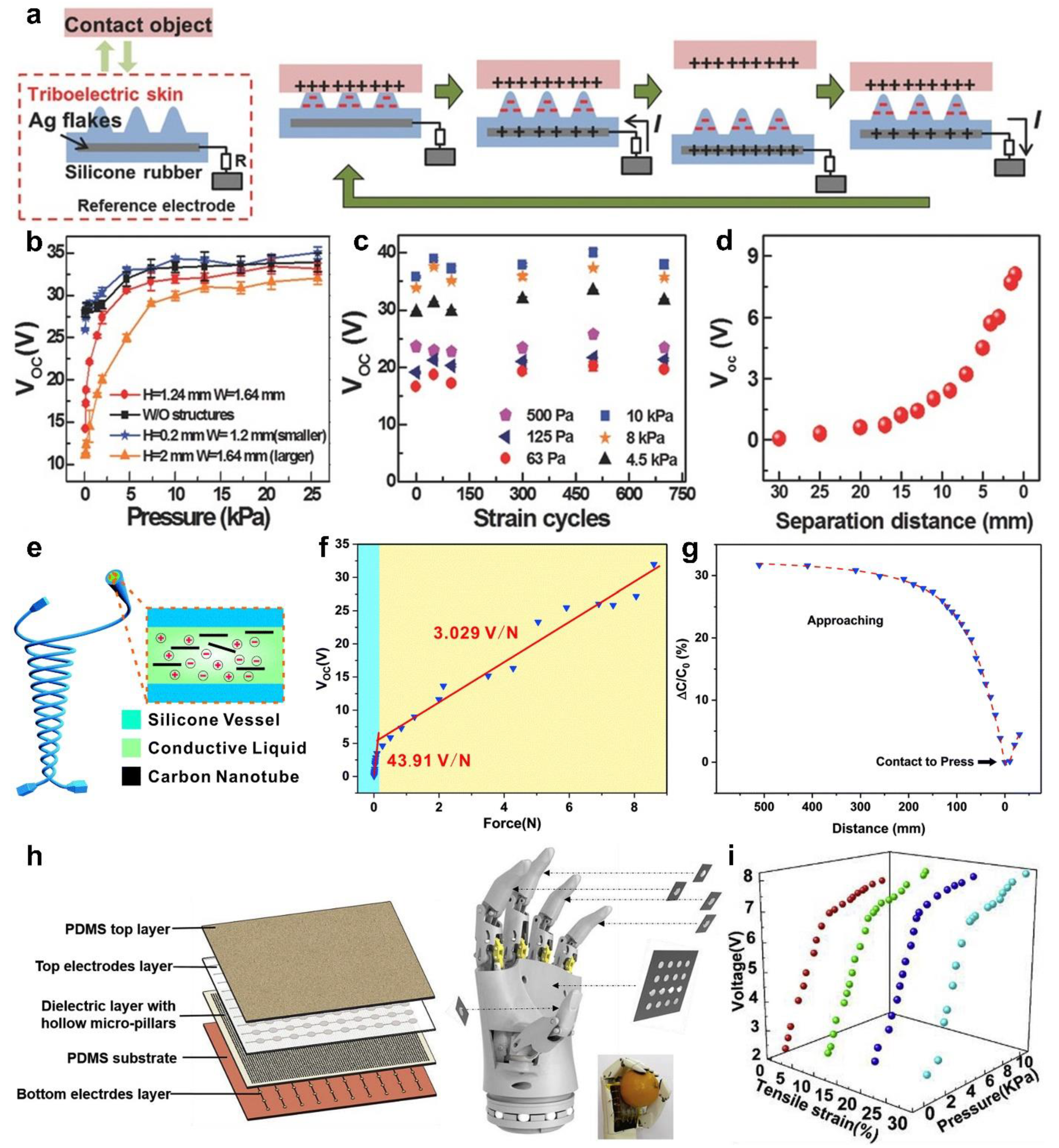
2.2. Pressure and Proximity Sensing
2.3. Pressure and Object Recognition
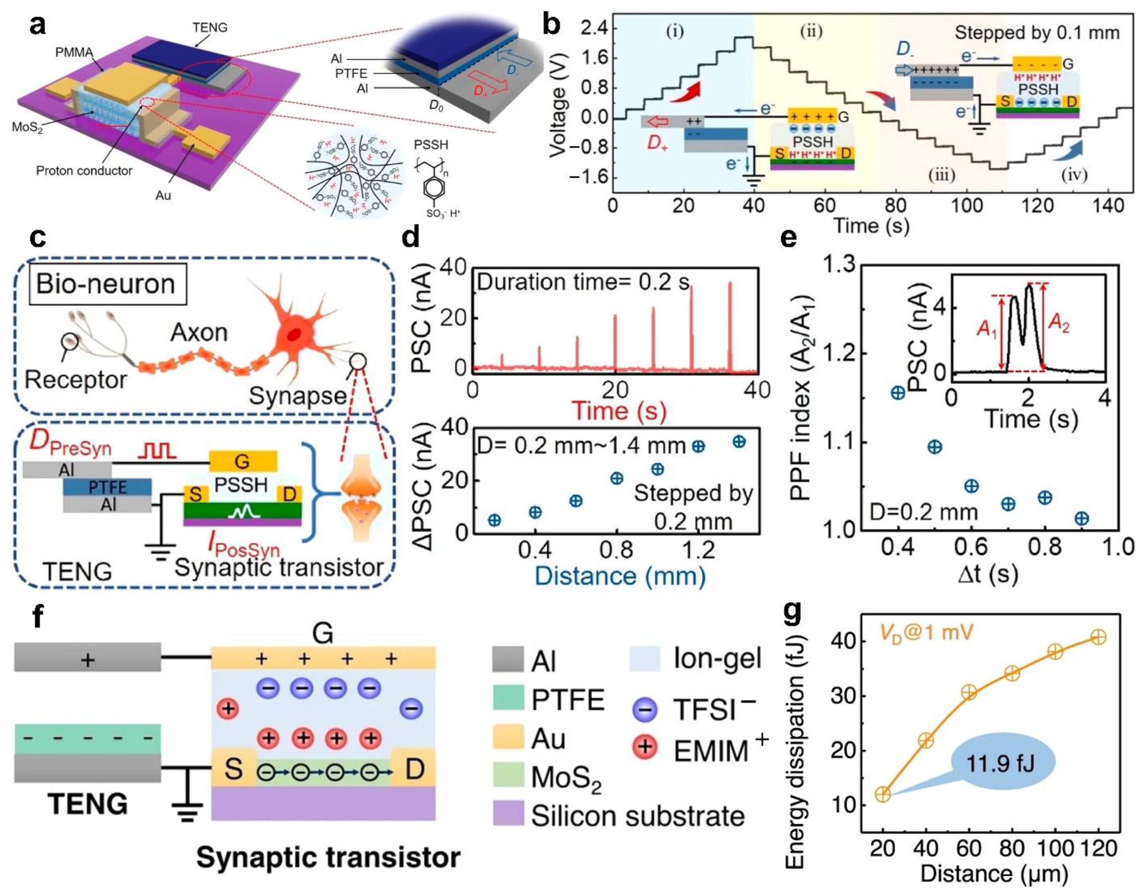
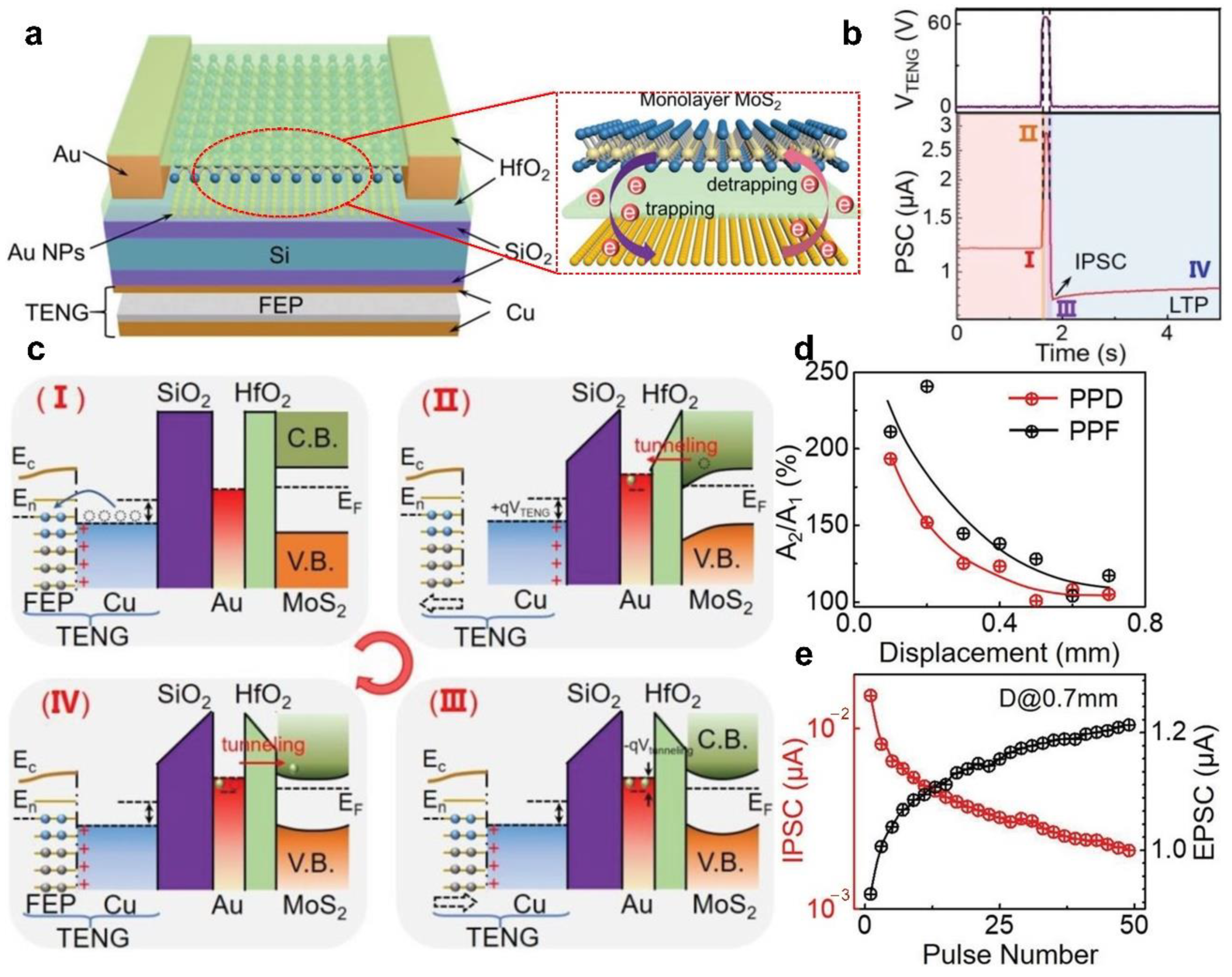
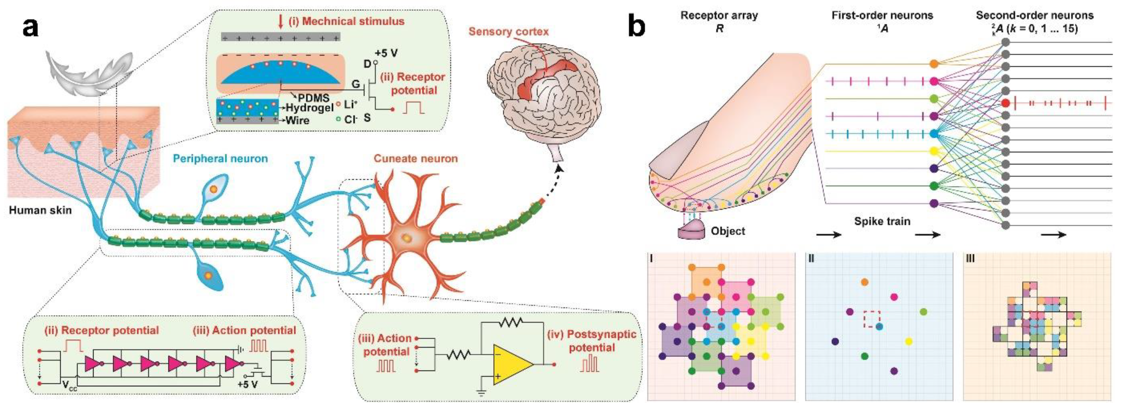
3. TENGs as Tactile Stimulators for Artificial Synapses
3.1. Transistor-Based Artificial Synapses
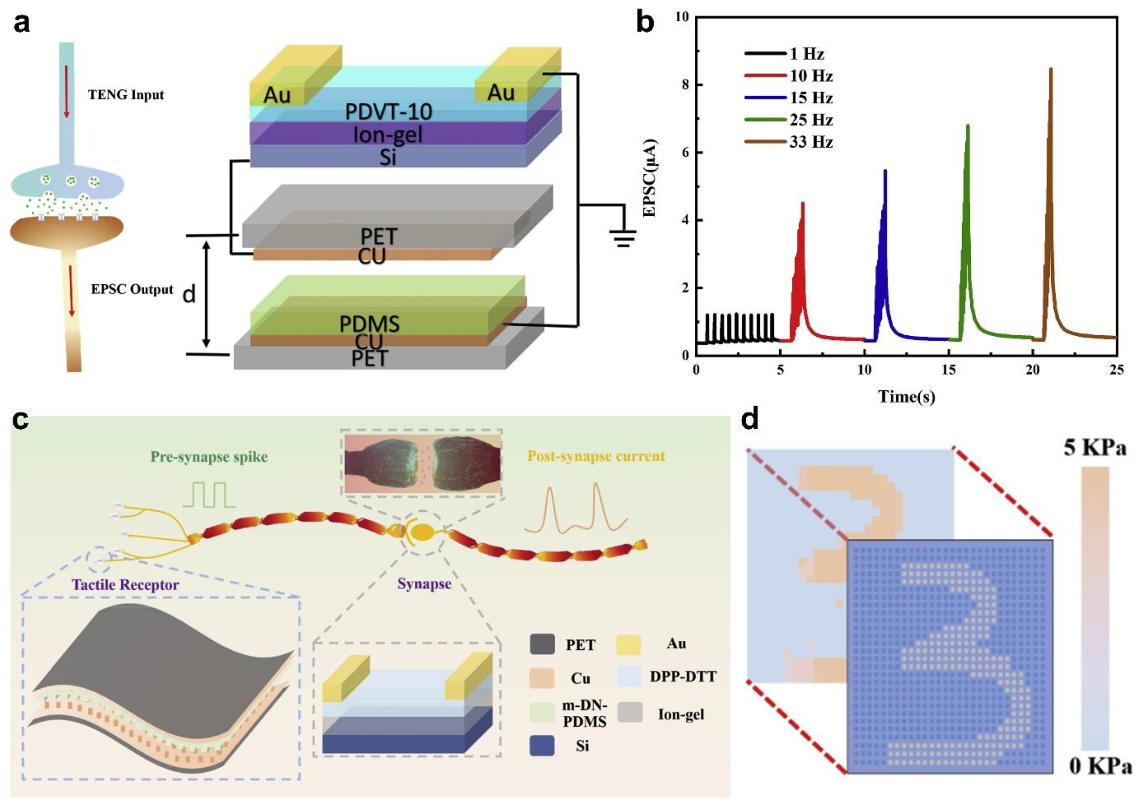
3.1.1. Electrolyte-Gate Synaptic Transistors
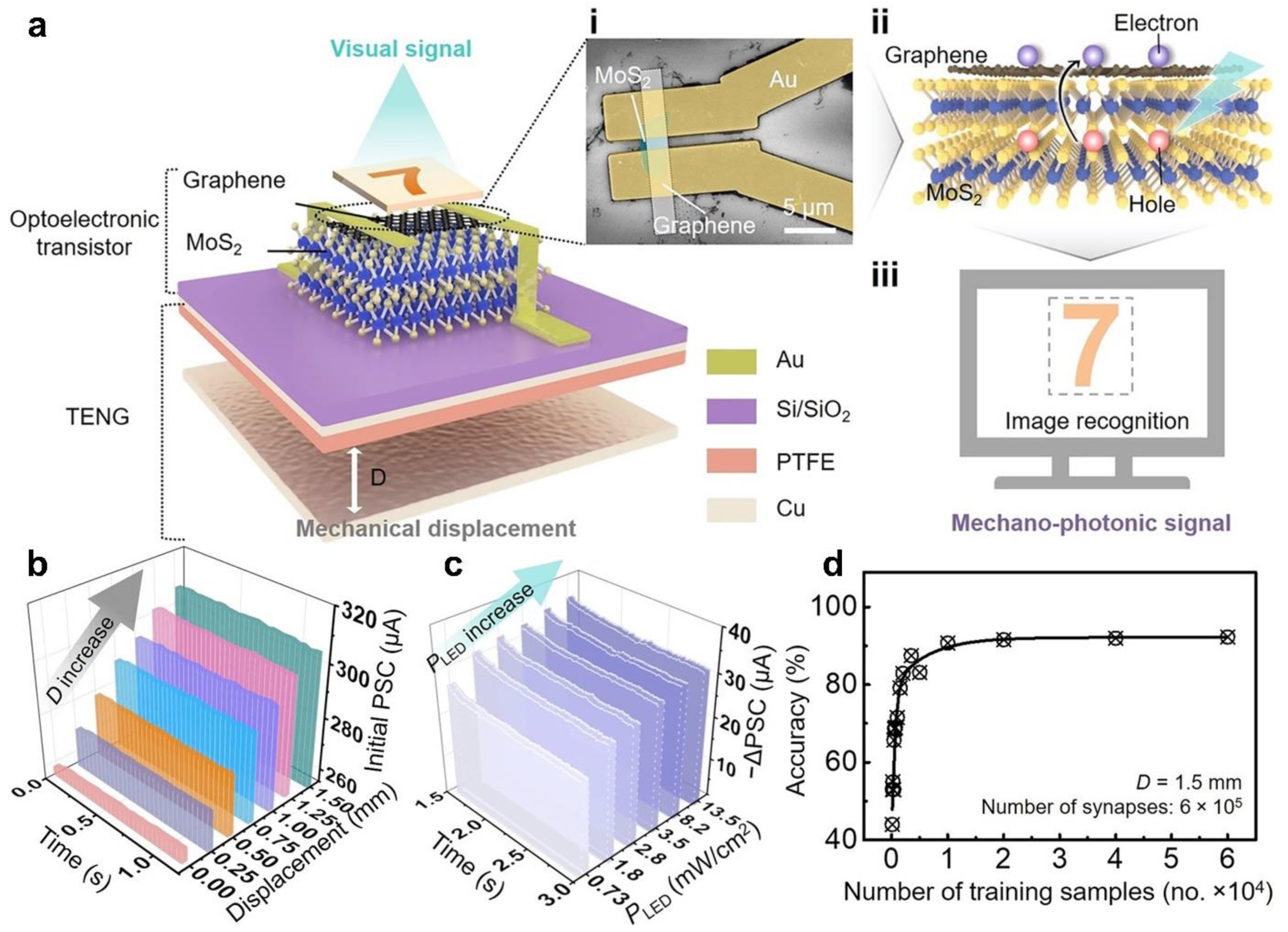
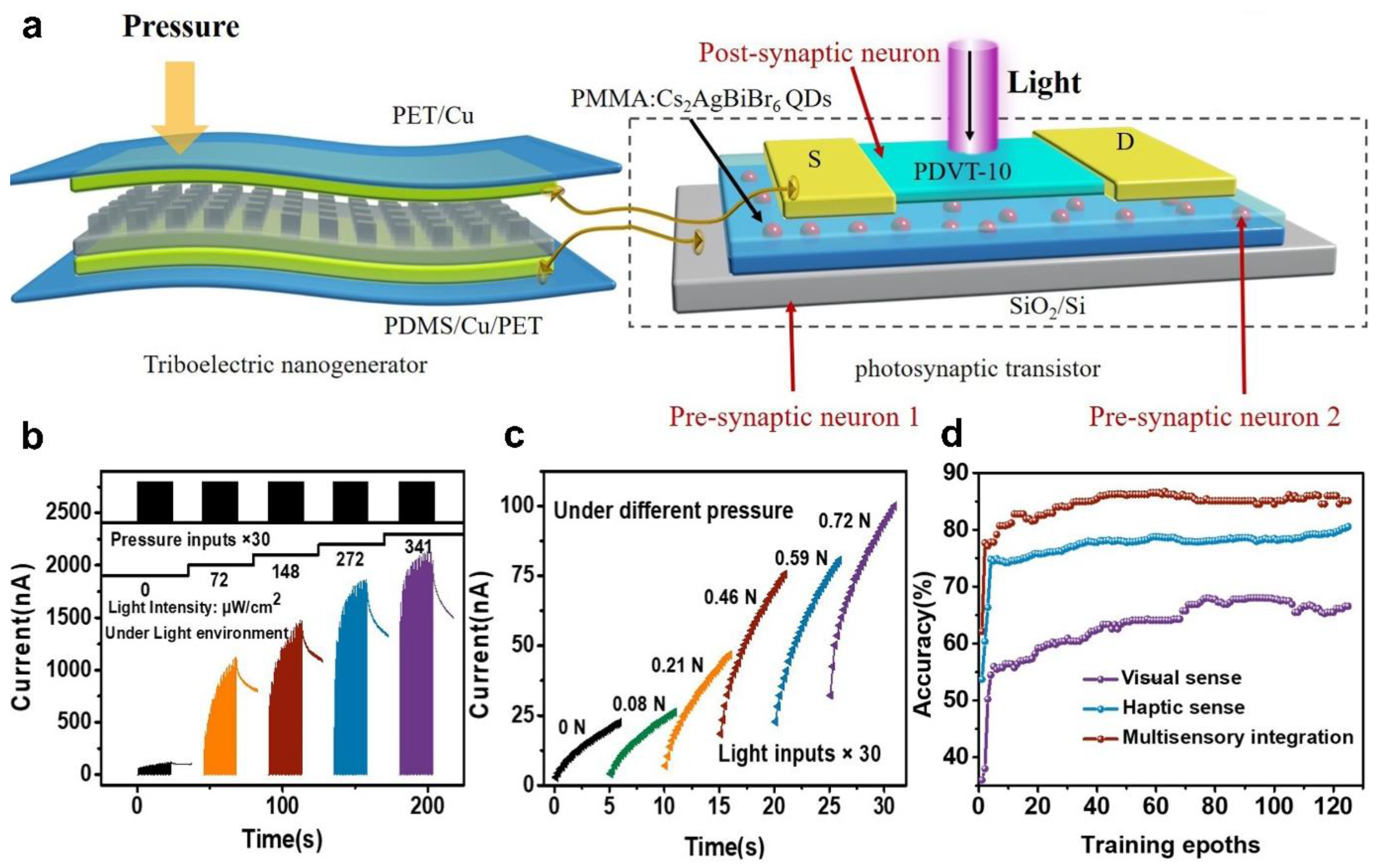
3.1.2. Optoelectronic Synaptic Transistors
3.1.3. Floating-Gate Synaptic Transistors
3.2. Reduced Graphene Oxides-Based Artificial Synapse
3.3. Integrated Circuit-Based Artificial Synapse and Nervous System
4. Summary and Perspectives
- Active tactile stimulators based on TENGs not only require high performance such as high sensitivity, high resolution, wide detection range, fast response, and good linearity, but also require functional characteristics such as stretchability, transparency, and self-healing. Although the tactile stimulators based on TENGs show ultra-high sensitivity under low pressure, the sensitivity decreases with the increase of pressure, which greatly limits measurement range. This is mainly because the output signal of the device is closely related to the contact area of the friction layer. Under low pressure, the contact area gradually increases as the pressure increases. When the pressure increases to a certain value, the contact area gradually saturates, which reduces the sensitivity. In addition, the characteristics such as stretchability, transparency, and self-healing are essential elements for the practical application of TENGs-based active tactile stimulators to complex environments. Therefore, the structure optimization of devices and the development of new materials to obtain superior comprehensive performance are still the research focus in the future.
- Facts have proven that the active tactile stimulators based on TENGs can realize multifunctional sensing, including pressure and temperature sensing, pressure, and proximity sensing, pressure, and object recognition. However, the currently reported TENGs-based active tactile stimulators are not fully capable of simultaneously sensing more external stimuli similar to human skin in practical applications, since human skin has a variety of sensory receptors, such as mechanoreceptors, pain receptors, cold receptors, warm receptors. In addition to the research on structure and materials of the devices, integrating the TENG with other sensing mechanisms into a sensing unit to respond to multiple stimuli in a complex environment is also research topic in the future.
- The human brain is composed of 1011 neurons and 1015 synapses, which can handle various complex tasks with a small volume occupation and an ultra-low power consumption. However, current research mainly focuses on the single synaptic device based on TENG that can mimic part of the synaptic behavior, but there are few reports on the array device that mimic the parallel operation of the brain. This is because the high-density integration and miniaturization of the array device, which leads to huge challenges in micro/nano manufacturing technology. Therefore, how to ensure the consistency of the performance of each unit of the array device is one of the main problems. Another thorny issue is that high-density integrated array device is prone to signal interference between units, which affect the output signal of the array device. In future research, it is necessary to optimize the preparation process and design an effective anti-interference scheme to achieve large-scale parallel work and high plasticity of the array devices.
- The effective combination of the triboelectric potential and synaptic transistor not only establishes the active sensing mechanism between external stimuli and the device, but also effectively reduces the total power consumption of the device. Although the device has successfully mimicked the function of receptors and synapses in biological systems, but there is still a long way to go to realize a complete bionic perception system, including signal perception, signal transmission, signal processing and signal feedback. Therefore, it is necessary to design a variety of different stimulators by using different mechanisms or structures to mimic tactile, auditory, visual, and other sensory functions, and make them work synergistically to update synaptic weights to achieve interactive neuromorphic computation. In addition, it will be an effective strategy to integrate the device with the signal processing circuit and build a complete bionic sensing closed-loop system driven by new software or algorithm.
Author Contributions
Funding
Institutional Review Board Statement
Informed Consent Statement
Data Availability Statement
Conflicts of Interest
References
- Mannsfeld, S.C.B.; Tee, B.C.; Stoltenberg, R.M.; Chen, C.V.H.; Barman, S.; Muir, B.V.O.; Sokolov, A.N.; Reese, C.; Bao, Z. Highly sensitive flexible pressure sensors with microstructured rubber dielectric layers. Nat. Mater. 2010, 9, 859–864. [Google Scholar] [CrossRef] [PubMed]
- Lipomi, D.J.; Vosgueritchian, M.; Tee, B.C.; Hellstrom, S.L.; Lee, J.A.; Fox, C.H.; Bao, Z. Skin-like pressure and strain sensors based on transparent elastic films of carbon nanotubes. Nat. Nanotechnol. 2011, 6, 788–792. [Google Scholar] [CrossRef] [PubMed]
- Pan, L.; Chortos, A.; Yu, G.; Wang, Y.; Isaacson, S.; Allen, R.; Shi, Y.; Dauskardt, R.; Bao, Z. An ultra-sensitive resistive pressure sensor based on hollow-sphere microstructure induced elasticity in conducting polymer film. Nat. Commun. 2014, 5, 3002. [Google Scholar] [CrossRef] [PubMed] [Green Version]
- Tee, B.C.; Chortos, A.; Berndt, A.; Nguyen, A.K.; Tom, A.; McGuire, A.; Lin, Z.C.; Tien, K.; Bae, W.; Wang, H.; et al. A skin-inspired organic digital mechanoreceptor. Science 2015, 350, 313–316. [Google Scholar] [CrossRef] [Green Version]
- Wan, Y.; Wang, Y.; Guo, C.F. Recent progresses on flexible tactile sensors. Mater. Today Phys. 2017, 1, 61–73. [Google Scholar] [CrossRef]
- Yang, T.; Xie, D.; Li, Z.; Zhu, H. Recent advances in wearable tactile sensors: Materials, sensing mechanisms, and device performance. Mater. Sci. Eng. R Rep. 2017, 115, 1–37. [Google Scholar] [CrossRef]
- Liu, Y.; Bao, R.; Tao, J.; Li, J.; Dong, M.; Pan, C. Recent progress in tactile sensors and their applications in intelligent systems. Sci. Bull. 2020, 65, 70–88. [Google Scholar] [CrossRef] [Green Version]
- Zhu, M.; He, T.; Lee, C. Technologies toward next generation human machine interfaces: From machine learning enhanced tactile sensing to neuromorphic sensory systems. Appl. Phys. Rev. 2020, 7, 031305. [Google Scholar] [CrossRef]
- Pacchierotti, C.; Sinclair, S.; Solazzi, M.; Frisoli, A.; Hayward, V.; Prattichizzo, D. Wearable haptic systems for the fingertip and the hand: Taxonomy, review, and perspectives. IEEE Trans. Haptics 2017, 10, 580–600. [Google Scholar] [CrossRef] [Green Version]
- Hwang, Y.; Candler, R.N. Non-planar PDMS microfluidic channels and actuators: A review. Lab Chip 2017, 17, 3948–3959. [Google Scholar] [CrossRef]
- Fan, F.; Tian, Z.; Lin Wang, Z. Flexible triboelectric generator. Nano Energy 2012, 1, 328–334. [Google Scholar] [CrossRef]
- Wang, Z.L. On Maxwell’s displacement current for energy and sensors: The origin of nanogenerators. Mater. Today 2017, 20, 74–82. [Google Scholar] [CrossRef]
- Luo, J.; Wang, Z.L. Recent progress of triboelectric nanogenerators: From fundamental theory to practical applications. EcoMat 2020, 2, e12059. [Google Scholar] [CrossRef]
- Shao, J.; Willatzen, M.; Wang, Z.L. Theoretical modeling of triboelectric nanogenerators (TENGs). J. Appl. Phys. 2020, 128, 111101. [Google Scholar] [CrossRef]
- Wang, Z.L. Triboelectric nanogenerator (TENG)-sparking an energy and sensor revolution. Adv. Energy Mater. 2020, 10, 2000137. [Google Scholar] [CrossRef] [Green Version]
- Wang, Z.L. From contact-electrification to triboelectric nanogenerators. Rep. Prog. Phys. 2021, 84, 096502. [Google Scholar] [CrossRef]
- Zhu, G.; Lin, Z.; Jing, Q.; Bai, P.; Pan, C.; Yang, Y.; Zhou, Y.; Wang, Z.L. Toward large-scale energy harvesting by a nanoparticle-enhanced triboelectric nanogenerator. Nano Lett. 2013, 13, 847–853. [Google Scholar] [CrossRef]
- Yang, Y.; Zhou, Y.S.; Zhang, H.; Liu, Y.; Lee, S.; Wang, Z.L. A single-electrode based triboelectric nanogenerator as self-powered tracking system. Adv. Mater. 2013, 25, 6594–6601. [Google Scholar] [CrossRef]
- Zhu, G.; Chen, J.; Liu, Y.; Bai, P.; Zhou, Y.S.; Jing, Q.; Pan, C.; Wang, Z.L. Linear-grating triboelectric generator based on sliding electrification. Nano Lett. 2013, 13, 2282–2289. [Google Scholar] [CrossRef]
- Zhu, G.; Chen, J.; Zhang, T.; Jing, Q.; Wang, Z.L. Radial-arrayed rotary electrification for high performance triboelectric generator. Nat. Commun. 2014, 5, 3426. [Google Scholar] [CrossRef]
- Yang, Y.; Zhang, H.; Lin, Z.; Zhou, Y.S.; Jing, Q.; Su, Y.; Yang, J.; Chen, J.; Hu, C.; Wang, Z.L. Human skin based triboelectric nanogenerators for harvesting biomechanical energy and as self-powered active tactile sensor system. ACS Nano 2013, 7, 9213–9222. [Google Scholar] [CrossRef] [PubMed] [Green Version]
- Zhu, G.; Yang, W.Q.; Zhang, T.; Jing, Q.; Chen, J.; Zhou, Y.S.; Bai, P.; Wang, Z.L. Self-powered, ultrasensitive, flexible tactile sensors based on contact electrification. Nano Lett. 2014, 14, 3208–3213. [Google Scholar] [CrossRef] [PubMed]
- Wang, S.; Lin, L.; Xie, Y.; Jing, Q.; Niu, S.; Wang, Z.L. Sliding-triboelectric nanogenerators based on in-plane charge-separation mechanism. Nano Lett. 2013, 13, 2226–2233. [Google Scholar] [CrossRef] [PubMed] [Green Version]
- Zhu, G.; Zhou, Y.S.; Bai, P.; Meng, X.S.; Jing, Q.; Chen, J.; Wang, Z.L. A shape-adaptive thin-film-based approach for 50% high-efficiency energy generation through micro-grating sliding electrification. Adv. Mater. 2014, 26, 3788–3796. [Google Scholar] [CrossRef] [PubMed]
- Lin, L.; Wang, S.; Xie, Y.; Jing, Q.; Niu, S.; Hu, Y.; Wang, Z.L. Segmentally structured disk triboelectric nanogenerator for harvesting rotational mechanical energy. Nano Lett. 2013, 13, 2916–2923. [Google Scholar] [CrossRef]
- Xu, S.; Fu, X.; Liu, G.; Tong, T.; Bu, T.; Wang, Z.L.; Zhang, C. Comparison of applied torque and energy conversion efficiency between rotational triboelectric nanogenerator and electromagnetic generator. iScience 2021, 24, 102318. [Google Scholar] [CrossRef]
- Lin, L.; Xie, Y.; Wang, S.; Wu, W.; Niu, S.; Wen, X.; Wang, Z.L. Triboelectric active sensor array for self-powered static and dynamic pressure detection and tactile imaging. ACS Nano 2013, 7, 8266–8274. [Google Scholar] [CrossRef]
- Chen, J.; Zhu, G.; Yang, W.; Jing, Q.; Bai, P.; Yang, Y.; Hou, T.; Wang, Z.L. Harmonic-resonator-based triboelectric nanogenerator as a sustainable power source and a self-powered active vibration sensor. Adv. Mater. 2013, 25, 6094–6099. [Google Scholar] [CrossRef]
- Yang, J.; Chen, J.; Liu, Y.; Yang, W.; Su, Y.; Wang, Z.L. Triboelectrification-based organic film nanogenerator for acoustic energy harvesting and self-powered active acoustic sensing. ACS Nano 2014, 8, 2649–2657. [Google Scholar] [CrossRef]
- Wang, Z.L. Triboelectric nanogenerators as new energy technology and self-powered sensors-principles, problems and perspectives. Faraday Discuss. 2014, 176, 447–458. [Google Scholar] [CrossRef]
- Wang, Z.L.; Chen, J.; Lin, L. Progress in triboelectric nanogenerators as a new energy technology and self-powered sensors. Energy Environ. Sci. 2015, 8, 225–2282. [Google Scholar] [CrossRef]
- Wen, Z.; Yeh, M.H.; Guo, H.; Wang, J.; Zi, Y.; Xu, W.; Deng, J.; Zhu, L.; Wang, X.; Hu, C.; et al. Self-powered textile for wearable electronics by hybridizing fiber-shaped nanogenerators, solar cells, and supercapacitors. Sci. Adv. 2016, 2, e1600097. [Google Scholar] [CrossRef] [PubMed] [Green Version]
- Chen, J.; Zhu, G.; Yang, J.; Jing, Q.; Bai, P.; Yang, W.; Qi, X.; Su, Y.; Wang, Z.L. Personalized keystroke dynamics for self-powered human-machine Interfacing. ACS Nano 2015, 9, 105–116. [Google Scholar] [CrossRef]
- Wang, Z.L.; Jiang, T.; Xu, L. Toward the blue energy dream by triboelectric nanogenerator networks. Nano Energy 2017, 39, 9–23. [Google Scholar] [CrossRef]
- Cheng, J.; Ding, W.; Zi, Y.; Lu, Y.; Ji, L.; Liu, F.; Wu, C.; Wang, Z.L. Triboelectric microplasma powered by mechanical stimuli. Nat. Commun. 2018, 9, 3733. [Google Scholar] [CrossRef] [PubMed]
- Wu, C.; Wang, A.C.; Ding, W.; Guo, H.; Wang, Z.L. Triboelectric Nanogenerator: A Foundation of the Energy for the New Era. Adv. Energy Mater. 2019, 9, 1802906. [Google Scholar] [CrossRef]
- Luo, J.; Fan, F.R.; Zhou, T.; Tang, W.; Xue, F.; Wang, Z.L. Ultrasensitive self-powered pressure sensing system. Extrem. Mech. Lett. 2015, 2, 28–36. [Google Scholar] [CrossRef]
- Hong, S.Y.; Lee, Y.H.; Park, H.; Jin, S.W.; Jeong, Y.R.; Yun, J.; You, I.; Zi, G.; Ha, J.S. Stretchable active matrix temperature sensor array of polyaniline nanofibers for electronic skin. Adv. Mater. 2016, 28, 930–935. [Google Scholar] [CrossRef]
- Wang, X.; Que, M.; Chen, M.; Han, X.; Li, X.; Pan, C.; Wang, Z.L. Full dynamic-range pressure sensor matrix based on optical and electrical dual-mode Sensing. Adv. Mater. 2017, 29, 1605817. [Google Scholar] [CrossRef]
- Ha, M.; Lim, S.; Cho, S.; Lee, Y.; Na, S.; Baig, C.; Ko, H. Skin-inspired hierarchical polymer architectures with gradient stiffness for spacer-free, ultrathin, and highly sensitive triboelectric sensors. ACS Nano 2018, 12, 3964–3974. [Google Scholar] [CrossRef]
- Fan, F.; Lin, L.; Zhu, G.; Wu, W.; Zhang, R.; Wang, Z.L. Transparent triboelectric nanogenerators and self-powered pressure sensors based on micropatterned plastic films. Nano Lett. 2012, 12, 3109–3114. [Google Scholar] [CrossRef] [PubMed] [Green Version]
- Yi, F.; Lin, L.; Niu, S.; Yang, J.; Wu, W.; Wang, S.; Liao, Q.; Zhang, Y.; Wang, Z.L. Self-powered trajectory, velocity, and acceleration tracking of a moving object/body using a triboelectric sensor. Adv. Funct. Mater. 2014, 24, 7488–7494. [Google Scholar] [CrossRef]
- Wang, X.; Zhang, H.; Dong, L.; Han, X.; Du, W.; Zhai, J.; Pan, C.; Wang, Z.L. Self-powered high-resolution and pressure-sensitive triboelectric sensor matrix for real-time tactile mapping. Adv. Mater. 2016, 28, 2896–2903. [Google Scholar] [CrossRef] [PubMed]
- Zhao, J.; Guo, H.; Pang, Y.K.; Xi, F.; Yang, Z.W.; Liu, G.; Guo, T.; Dong, G.; Zhang, C.; Wang, Z.L. Flexible organic tribotronic transistor for pressure and magnetic sensing. ACS Nano 2017, 11, 11566–11573. [Google Scholar] [CrossRef]
- Rong, X.; Zhao, J.; Guo, H.; Zhen, G.; Yu, J.; Zhang, C.; Dong, G. Material recognition sensor array by electrostatic induction and triboelectric effects. Adv. Mater. Technol. 2020, 5, 2000641. [Google Scholar] [CrossRef]
- Kim, B.; Hwang, H.; Woo, J.; Lee, W.; Lee, T.; Kang, C.; Nahm, S. Nanogenerator-induced synaptic plasticity and metaplasticity of bio-realistic artificial synapses. NPG Asia Mater. 2017, 9, e381. [Google Scholar] [CrossRef] [Green Version]
- Li, L.; Li, J.; Jiang, D.; Fu, W.; Zhu, W.; Zhang, J. Self-powered synaptic transistor for artificial perception. IEEE Electron Device Lett. 2021, 42, 1002–1005. [Google Scholar] [CrossRef]
- Bu, T.; Xiao, T.; Yang, Z.; Liu, G.; Fu, X.; Nie, J.; Guo, T.; Pang, Y.; Zhao, J.; Xi, F.; et al. Stretchable triboelectric-photonic smart skin for tactile and gesture sensing. Adv. Mater. 2018, 30, 1800066. [Google Scholar] [CrossRef]
- Liu, Y.; Zhong, J.; Li, E.; Yang, H.; Wang, X.; Lai, D.; Chen, H.; Guo, T. Self-powered artificial synapses actuated by triboelectric nanogenerator. Nano Energy 2019, 60, 377–384. [Google Scholar] [CrossRef]
- Wu, C.; Kim, T.W.; Park, J.H.; Koo, B.; Sung, S.; Shao, J.; Zhang, C.; Wang, Z.L. self-powered tactile sensor with learning and memory. ACS Nano 2020, 14, 1390–1398. [Google Scholar] [CrossRef]
- Yu, J.; Gao, G.; Huang, J.; Yang, X.; Han, J.; Zhang, H.; Chen, Y.; Zhao, C.; Sun, Q.; Wang, Z.L. Contact-electrification-activated artificial afferents at femtojoule energy. Nat. Commun. 2021, 12, 1581. [Google Scholar] [CrossRef] [PubMed]
- Karmakar, S.; Kumbhakar, P.; Maity, K.; Mandal, D.; Kumbhakar, P. Development of flexible self-charging triboelectric power cell on paper for temperature and weight sensing. Nano Energy 2019, 63, 103831. [Google Scholar] [CrossRef]
- Wang, Y.; Zhang, L.; Lu, A. Highly stretchable, transparent cellulose/PVA composite hydrogel for multiple sensing and triboelectric nanogenerators. J. Mater. Chem. A 2020, 8, 13935–13941. [Google Scholar] [CrossRef]
- Cheng, Y.; Wu, D.; Hao, S.; Jie, Y.; Cao, X.; Wang, N.; Wang, Z.L. Highly stretchable triboelectric tactile sensor for electronic skin. Nano Energy 2019, 64, 103907. [Google Scholar] [CrossRef]
- Song, L.; Zhang, Z.; Xun, X.; Xu, L.; Gao, F.; Zhao, X.; Kang, Z.; Liao, Q.; Zhang, Y. Fully organic self-powered electronic skin with multifunctional and highly robust sensing capability. Research 2021, 2021, 9801832. [Google Scholar] [CrossRef]
- Rao, J.; Chen, Z.; Zhao, D.; Ma, R.; Yi, W.; Zhang, C.; Liu, D.; Chen, X.; Yang, Y.; Wang, X.; et al. Tactile electronic skin to simultaneously detect and distinguish between temperature and pressure based on a triboelectric nanogenerator. Nano Energy 2020, 75, 105073. [Google Scholar] [CrossRef]
- Ma, M.; Zhang, Z.; Zhao, Z.; Liao, Q.; Kang, Z.; Gao, F.; Zhao, X.; Zhang, Y. Self-powered flexible antibacterial tactile sensor based on triboelectric-piezoelectric-pyroelectric multi-effect coupling mechanism. Nano Energy 2019, 66, 104105. [Google Scholar] [CrossRef]
- Wang, Y.; Wu, H.; Xu, L.; Zhang, H.; Yang, Y.; Wang, Z.L. Hierarchically patterned self-powered sensors for multifunctional tactile sensing. Sci. Adv. 2020, 6, eabb9083. [Google Scholar] [CrossRef]
- Lai, Y.; Deng, J.; Liu, R.; Hsiao, Y.; Zhang, S.L.; Peng, W.; Wu, H.; Wang, X.; Wang, Z.L. Actively perceiving and responsive soft robots enabled by self-powered, highly extensible, and highly sensitive triboelectric proximity- and pressure-sensing skins. Adv. Mater. 2018, 30, 1801114. [Google Scholar] [CrossRef]
- Yuan, Z.; Du, X.; Niu, H.; Li, N.; Shen, G.; Li, C.; Wang, Z.L. Motion recognition by a liquid filled tubular triboelectric nanogenerator. Nanoscale 2019, 11, 495–503. [Google Scholar] [CrossRef]
- Zhang, C.; Liu, S.; Huang, X.; Guo, W.; Li, Y.; Wu, H. A stretchable dual-mode sensor array for multifunctional robotic electronic skin. Nano Energy 2019, 62, 164–170. [Google Scholar] [CrossRef]
- Li, T.; Zou, J.; Xing, F.; Zhang, M.; Cao, X.; Wang, N.; Wang, Z.L. From dual-mode triboelectric nanogenerator to smart tactile sensor: A multiplexing design. ACS Nano 2017, 11, 3950–3956. [Google Scholar] [CrossRef] [PubMed]
- Jin, T.; Sun, Z.; Li, L.; Zhang, Q.; Zhu, M.; Zhang, Z.; Yuan, G.; Chen, T.; Tian, Y.; Hou, X.; et al. Triboelectric nanogenerator sensors for soft robotics aiming at digital twin applications. Nat. Commun 2020, 11, 5381. [Google Scholar] [CrossRef] [PubMed]
- Yang, J.; Ge, C.; Du, J.; Huang, H.; He, M.; Wang, C.; Lu, H.; Yang, G.; Jin, K. Artificial synapses emulated by an electrolyte-gated tungsten-oxide transistor. Adv. Mater. 2018, 30, 180154834. [Google Scholar] [CrossRef] [PubMed]
- Ling, H.; Koutsouras, D.A.; Kazemzadeh, S.; van de Burgt, Y.; Yan, F.; Gkoupidenis, P. Electrolyte-gated transistors for synaptic electronics, neuromorphic computing, and adaptable biointerfacing. Appl. Phys. Rev. 2020, 7, 011307. [Google Scholar] [CrossRef]
- Kim, S.H.; Hong, K.; Xie, W.; Lee, K.H.; Zhang, S.; Lodge, T.P.; Frisbie, C.D. Electrolyte-gated transistors for organic and printed electronics. Adv. Mater. 2013, 25, 1822–1846. [Google Scholar] [CrossRef]
- Li, J.; Tang, W.; Wang, Q.; Sun, W.; Zhang, Q.; Guo, X.; Wang, X.; Yan, F. Solution-processable organic and hybrid gate dielectrics for printed electronics. Mater. Sci. Eng. R Rep. 2018, 127, 1–36. [Google Scholar] [CrossRef]
- Dai, S.; Zhao, Y.; Wang, Y.; Zhang, J.; Fang, L.; Jin, S.; Shao, Y.; Huang, J. Recent Advances in Transistor-Based Artificial Synapses. Adv. Funct. Mater. 2019, 29, 1903700. [Google Scholar] [CrossRef]
- John, R.A.; Ko, J.; Kulkarni, M.R.; Tiwari, N.; Chien, N.A.; Ing, N.G.; Leong, W.L.; Mathews, N. Flexible ionic-electronic hybrid oxide synaptic TFTs with programmable dynamic plasticity for brain-inspired neuromorphic computing. Small 2017, 13, 32. [Google Scholar] [CrossRef]
- Liu, Y.; Yang, W.; Yan, Y.; Wu, X.; Wang, X.; Zhou, Y.; Hu, Y.; Chen, H.; Guo, T. Self-powered high-sensitivity sensory memory actuated by triboelectric sensory receptor for real-time neuromorphic computing. Nano Energy 2020, 75, 104930. [Google Scholar] [CrossRef]
- Zhang, C.; Li, S.; He, Y.; Chen, C.; Jiang, S.; Yang, X.; Wang, X.; Pan, L.; Wan, Q. Oxide synaptic transistors coupled with triboelectric nanogenerators for bio-inspired tactile sensing application. IEEE Electron Device Lett. 2020, 41, 617–620. [Google Scholar] [CrossRef]
- Jiang, J.; Guo, J.; Wan, X.; Yang, Y.; Xie, H.; Niu, D.; Yang, J.; He, J.; Gao, Y.; Wan, Q. 2D MoS2 neuromorphic devices for brain-like computational systems. Small 2017, 13, 1700933. [Google Scholar] [CrossRef] [PubMed]
- John, R.A.; Liu, F.; Chien, N.A.; Kulkarni, M.R.; Zhu, C.; Fu, Q.; Basu, A.; Liu, Z.; Mathews, N. Synergistic gating of electro-iono-photoactive 2D chalcogenide neuristors: Coexistence of hebbian and homeostatic synaptic metaplasticity. Adv. Mater. 2018, 30, 1800220. [Google Scholar] [CrossRef] [PubMed]
- Zhu, J.; Yang, Y.; Jia, R.; Liang, Z.; Zhu, W.; Rehman, Z.U.; Bao, L.; Zhang, X.; Cai, Y.; Song, L.; et al. Ion gated synaptic transistors based on 2D van der waals crystals with tunable diffusive dynamics. Adv. Mater. 2018, 30, 1800195. [Google Scholar] [CrossRef] [PubMed]
- Meng, Y.; Zhao, J.; Yang, X.; Zhao, C.; Qin, S.; Cho, J.H.; Zhang, C.; Sun, Q.; Wang, Z.L. Mechanosensation-active matrix based on direct-contact tribotronic planar graphene transistor array. ACS Nano 2018, 12, 9381–9389. [Google Scholar] [CrossRef]
- Wang, S.; Zhang, D.W.; Zhou, P. Two-dimensional materials for synaptic electronics and neuromorphic systems. Sci. Bull. 2019, 64, 1056–1066. [Google Scholar] [CrossRef] [Green Version]
- Wan, Q.; Sharbati, M.T.; Erickson, J.R.; Du, Y.; Xiong, F. Emerging artificial synaptic devices for neuromorphic computing. Adv. Mater. Technol. 2019, 4, 1900037. [Google Scholar] [CrossRef] [Green Version]
- Singh, E.; Singh, P.; Kim, K.S.; Yeom, G.Y.; Nalwa, H.S. Flexible molybdenum disulfide (MoS2) atomic layers for wearable electronics and optoelectronics. ACS Appl. Mater. Inter. 2019, 11, 11061–11105. [Google Scholar] [CrossRef]
- Seo, S.; Lee, J.; Lee, H.; Lee, H.W.; Oh, S.; Lee, J.J.; Heo, K.; Park, J. Recent progress in artificial synapses based on two-dimensional van der waals materials for brain-inspired computing. ACS Appl. Electron. 2020, 2, 371–388. [Google Scholar] [CrossRef]
- Zhang, H.; Yu, J.; Yang, X.; Gao, G.; Qin, S.; Sun, J.; Ding, M.; Jia, C.; Sun, Q.; Wang, Z.L. Ion gel capacitively coupled tribotronic gating for multiparameter distance sensing. ACS Nano 2020, 14, 3461–3468. [Google Scholar] [CrossRef]
- Xue, F.; Chen, L.; Wang, L.; Pang, Y.; Chen, J.; Zhang, C.; Wang, Z.L. MoS2 Tribotronic transistor for smart tactile switch. Adv. Funct. Mater. 2016, 26, 2104–2109. [Google Scholar] [CrossRef]
- Pang, Y.; Xue, F.; Wang, L.; Chen, J.; Luo, J.; Jiang, T.; Zhang, C.; Wang, Z.L. Tribotronic enhanced photoresponsivity of a MoS2 phototransistor. Adv. Sci. 2016, 3, 1500419. [Google Scholar] [CrossRef] [PubMed]
- Gao, G.; Yu, J.; Yang, X.; Pang, Y.; Zhao, J.; Pan, C.; Sun, Q.; Wang, Z.L. Triboiontronic transistor of MoS2. Adv. Mater. 2019, 31, 1806905. [Google Scholar] [CrossRef] [PubMed]
- Bao, L.; Zhu, J.; Yu, Z.; Jia, R.; Cai, Q.; Wang, Z.; Xu, L.; Wu, Y.; Yang, Y.; Cai, Y.; et al. Dual-gated MoS2 neuristor for neuromorphic computing. ACS Appl. Mater. Inter. 2019, 11, 41482–41489. [Google Scholar] [CrossRef]
- Yang, X.; Han, J.; Yu, J.; Chen, Y.; Zhang, H.; Ding, M.; Jia, C.; Sun, J.; Sun, Q.; Wang, Z.L. Versatile triboiontronic transistorvia proton conductor. ACS Nano 2020, 14, 8668–8677. [Google Scholar] [CrossRef]
- Kong, L.; Sun, J.; Qian, C.; Gou, G.; He, Y.; Yang, J.; Gao, Y. Ion-gel gated field-effect transistors with solution-processed oxide semiconductors for bioinspired artificial synapses. Org. Electron. 2016, 39, 64–70. [Google Scholar] [CrossRef]
- Bisri, S.Z.; Shimizu, S.; Nakano, M.; Iwasa, Y. Endeavor of iontronics: From fundamentals to applications of ion-controlled electronics. Adv. Mater. 2017, 29, 1607054. [Google Scholar] [CrossRef]
- Li, H.K.; Chen, T.P.; Liu, P.; Hu, S.G.; Liu, Y.; Zhang, Q.; Lee, P.S. A light-stimulated synaptic transistor with synaptic plasticity and memory functions based on InGaZnOx-Al2O3 thin film structure. J. Appl. Phys. 2016, 119, 244505. [Google Scholar] [CrossRef]
- Guo, Y.; Zhu, L. Recent progress in optoelectronic neuromorphic devices. Chin. Phys. B 2020, 29, 078502. [Google Scholar] [CrossRef]
- Wang, W.; Gao, S.; Li, Y.; Yue, W.; Kan, H.; Zhang, C.; Lou, Z.; Wang, L.; Shen, G. Artificial optoelectronic synapses based on TiNxO2-x/MoS2 heterojunction for neuromorphic computing and visual system. Adv. Funct. Mater. 2021, 31, 2101201. [Google Scholar] [CrossRef]
- Yu, J.; Yang, X.; Gao, G.; Xiong, Y.; Wang, Y.; Han, J.; Chen, Y.; Zhang, H.; Sun, Q.; Wang, Z.L. Bioinspired mechano-photonic artificial synapse based on graphene/MoS2 heterostructure. Sci. Adv. 2021, 7, eabd9117. [Google Scholar] [CrossRef] [PubMed]
- Roy, K.; Padmanabhan, M.; Goswami, S.; Sai, T.P.; Ramalingam, G.; Raghavan, S.; Ghosh, A. Graphene-MoS2 hybrid structures for multifunctional photoresponsive memory devices. Nat. Nanotechnol. 2013, 8, 826–830. [Google Scholar] [CrossRef] [PubMed]
- Wu, X.; Li, E.; Liu, Y.; Lin, W.; Yu, R.; Chen, G.; Hu, Y.; Chen, H.; Guo, T. Artificial multisensory integration nervous system with haptic and iconic perception behaviors. Nano Energy 2021, 85, 106000. [Google Scholar] [CrossRef]
- Yang, X.; Yu, J.; Zhao, J.; Chen, Y.; Gao, G.; Wang, Y.; Sun, Q.; Wang, Z.L. Mechanoplastic tribotronic floating-gate neuromorphic transistor. Adv. Funct. Mater. 2020, 30, 2002506. [Google Scholar] [CrossRef]
- Lee, D.; Hwang, E.; Lee, Y.; Choi, Y.; Kim, J.S.; Lee, S.; Cho, J.H. Multibit MoS2 photoelectronic memory with ultrahigh sensitivity. Adv. Mater. 2016, 28, 9196–9202. [Google Scholar] [CrossRef]
- Wu, C.; Kim, T.W.; Choi, H.Y. Reduced graphene-oxide acting as electron-trapping sites in the friction layer for giant triboelectric enhancement. Nano Energy 2017, 32, 542–550. [Google Scholar] [CrossRef]
- Chen, L.; Wen, C.; Zhang, S.; Wang, Z.L.; Zhang, Z. Artificial tactile peripheral nervous system supported by self-powered transducers. Nano Energy 2021, 82, 105680. [Google Scholar] [CrossRef]
- Eurich, C.W.; Schwegler, H. Coarse coding: Calculation of the resolution achieved by a population of large receptive field neurons. Biol. Cybern. 1997, 76, 357–363. [Google Scholar] [CrossRef]


| Reference | Size | Triboelectric Materials | Detection Signal | Sensitivity | Detection Range |
|---|---|---|---|---|---|
| [54] | 40 × 40 mm | (OMMT-CTAB) | Pressure: short-circuit current | 0.04 μA/kPa | 16~64 kPa |
| Temperature: short-circuit current | 0.59 μA/°C | 19.4~34.9 °C | |||
| [55] | 20 × 20 mm | Self-healing polymer | Pressure: output current | 3.55 nA/kPa | 0.12~100 kPa |
| Temperature: output current | 3.76 nA/°C | 20~60 °C | |||
| [56] | 15 × 10 mm | PDMS | Pressure: output voltage | 5.07 mV/Pa | 200~3650 Pa |
| Temperature: electrode resistance | β25/100 ≈ 1024 K | 25~100 °C | |||
| [57] | 50 × 50 mm | Ag NWs @PTFE | Pressure: output voltage | 0.092 V/kPa | 10.5~52 kPa |
| Temperature: output voltage | 0.11 V/°C | 10~45 °C | |||
| [58] | 10 × 10 mm | PTFE | Pressure: output current | 15.22 /kPa | 0~40 kPa |
| Temperature: output voltage | 35.2 μV/K | 25~60 °C |
Publisher’s Note: MDPI stays neutral with regard to jurisdictional claims in published maps and institutional affiliations. |
© 2022 by the authors. Licensee MDPI, Basel, Switzerland. This article is an open access article distributed under the terms and conditions of the Creative Commons Attribution (CC BY) license (https://creativecommons.org/licenses/by/4.0/).
Share and Cite
Zeng, J.; Zhao, J.; Li, C.; Qi, Y.; Liu, G.; Fu, X.; Zhou, H.; Zhang, C. Triboelectric Nanogenerators as Active Tactile Stimulators for Multifunctional Sensing and Artificial Synapses. Sensors 2022, 22, 975. https://doi.org/10.3390/s22030975
Zeng J, Zhao J, Li C, Qi Y, Liu G, Fu X, Zhou H, Zhang C. Triboelectric Nanogenerators as Active Tactile Stimulators for Multifunctional Sensing and Artificial Synapses. Sensors. 2022; 22(3):975. https://doi.org/10.3390/s22030975
Chicago/Turabian StyleZeng, Jianhua, Junqing Zhao, Chengxi Li, Youchao Qi, Guoxu Liu, Xianpeng Fu, Han Zhou, and Chi Zhang. 2022. "Triboelectric Nanogenerators as Active Tactile Stimulators for Multifunctional Sensing and Artificial Synapses" Sensors 22, no. 3: 975. https://doi.org/10.3390/s22030975
APA StyleZeng, J., Zhao, J., Li, C., Qi, Y., Liu, G., Fu, X., Zhou, H., & Zhang, C. (2022). Triboelectric Nanogenerators as Active Tactile Stimulators for Multifunctional Sensing and Artificial Synapses. Sensors, 22(3), 975. https://doi.org/10.3390/s22030975