
Signal Processing Platform for Long-Range Multi-Spectral Electro-Optical Systems

 , , and
Abstract
:1. Introduction
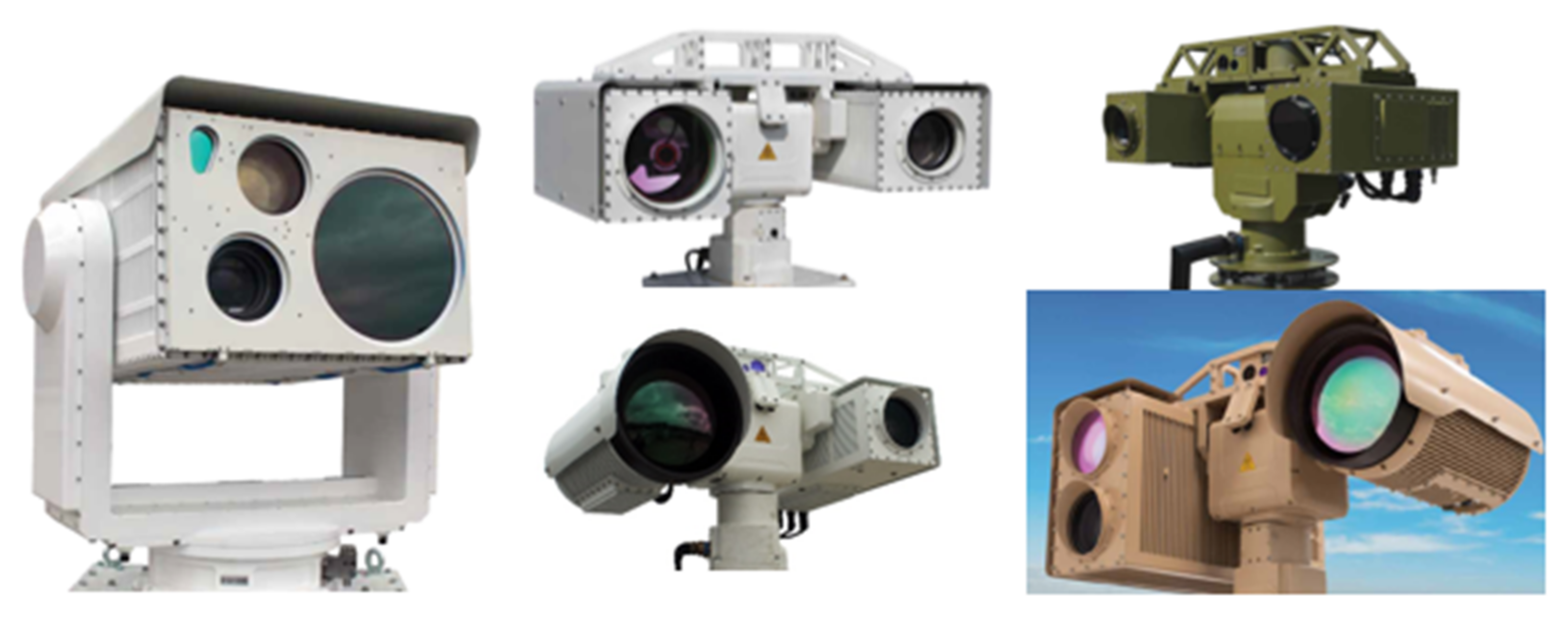
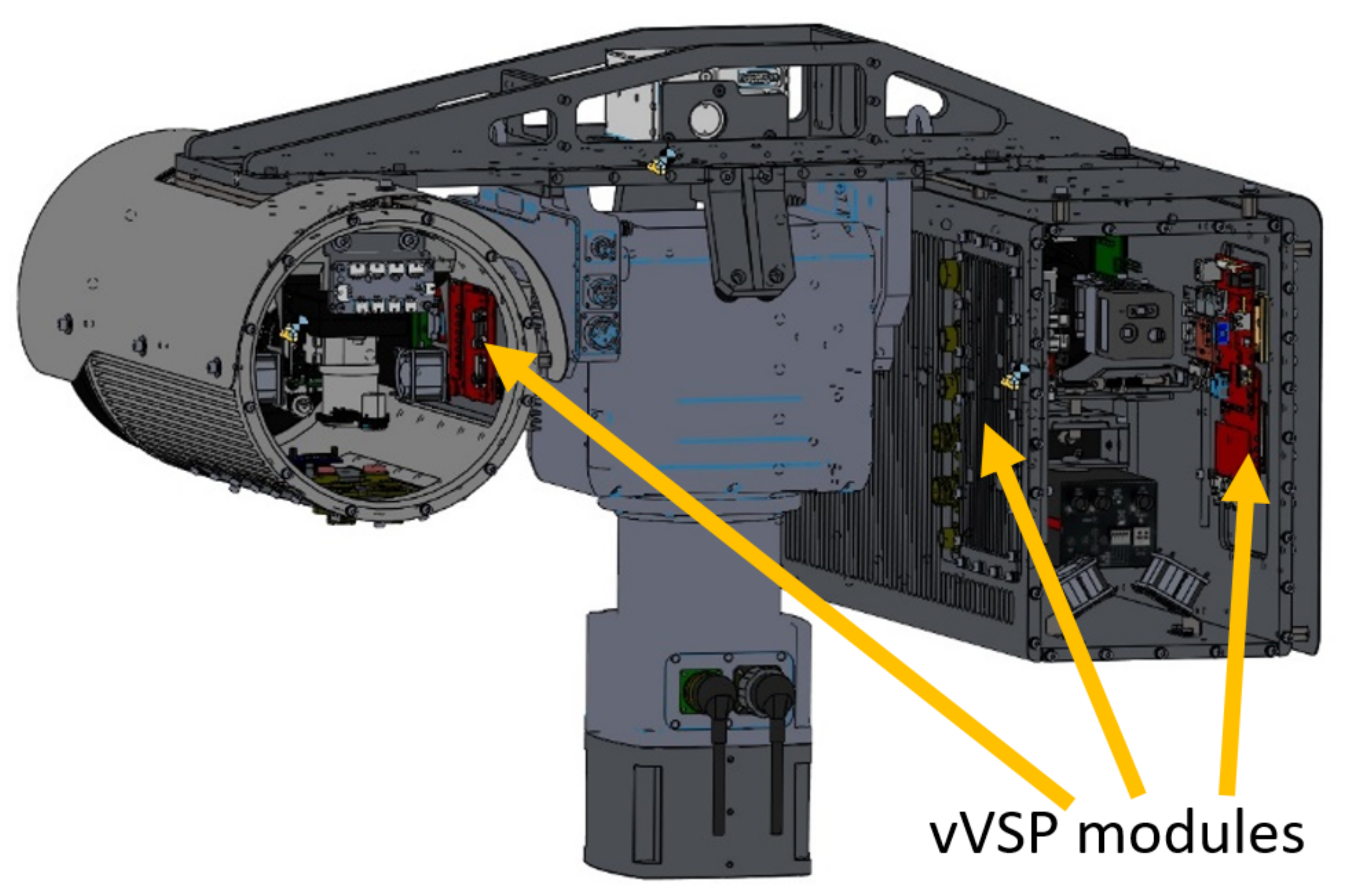
- Pan-Tilt positioner with mounted mechanical housing;
- Thermal infrared camera with a suitable lens covering the infrared (MWIR) or long-wave infrared (LWIR) part of the spectrum;
- Short-wave infrared camera with a suitable lens for the short-wave infrared (SWIR) part of the spectrum;
- Lowlight camera with a suitable lens for the visible part of the spectrum;
- Digital magnetic compass (DMC);
- Global Positioning System (GPS);
- Laser range finder (LRF);
- Inertial Measurement Unit (IMU);
- Signal processing module with built-in algorithms and appropriate software.
2. Description of VVSP Module
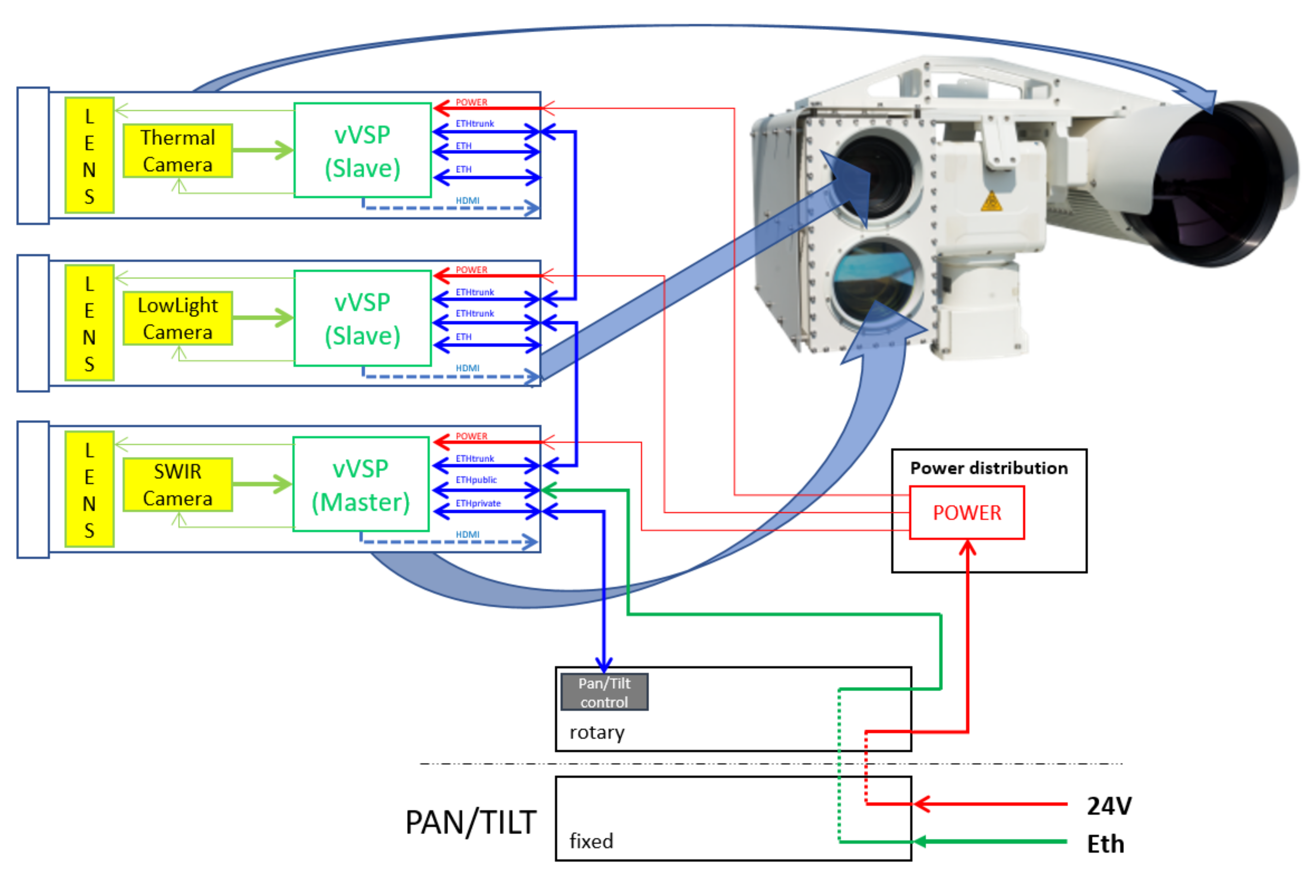
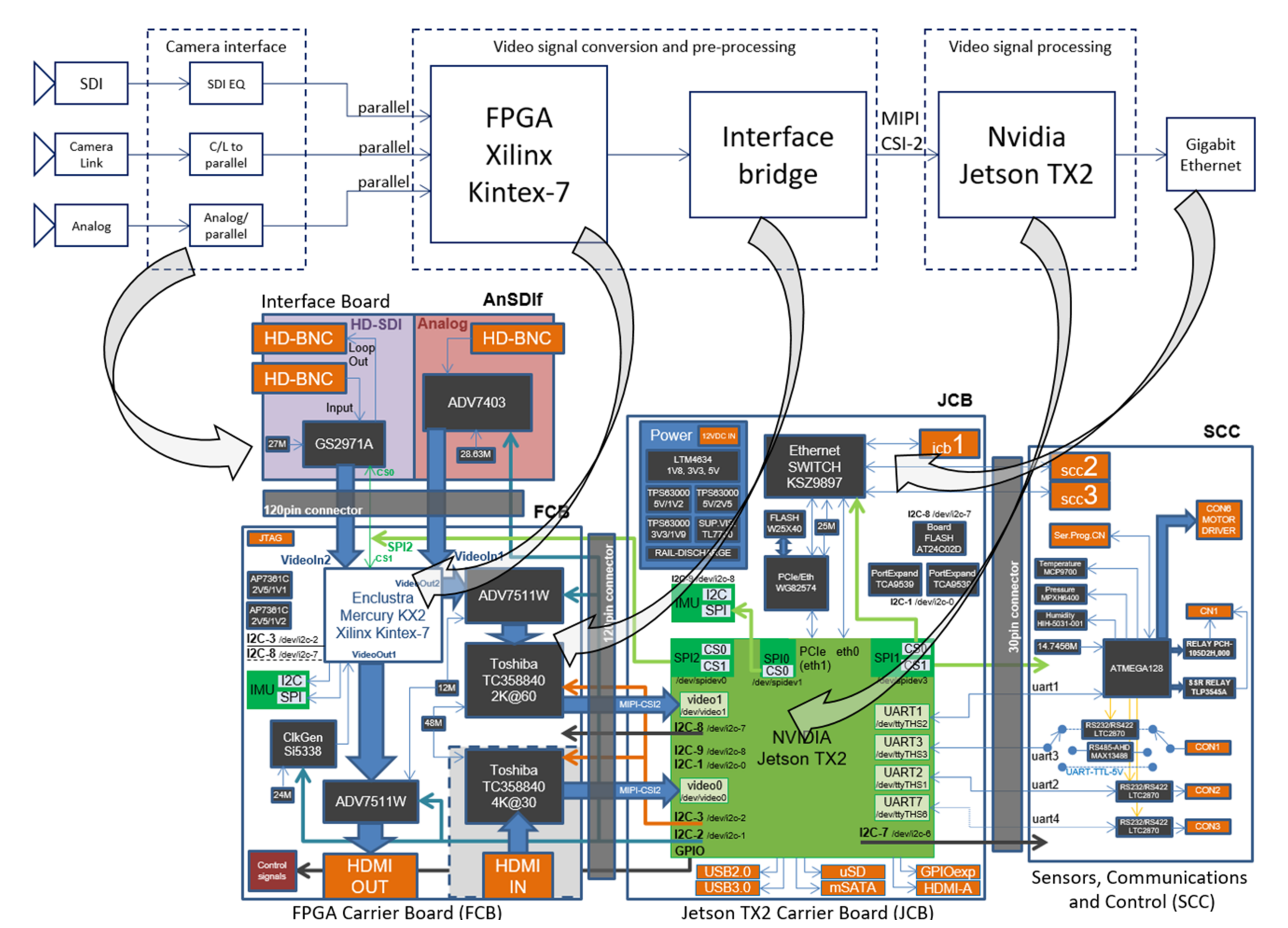
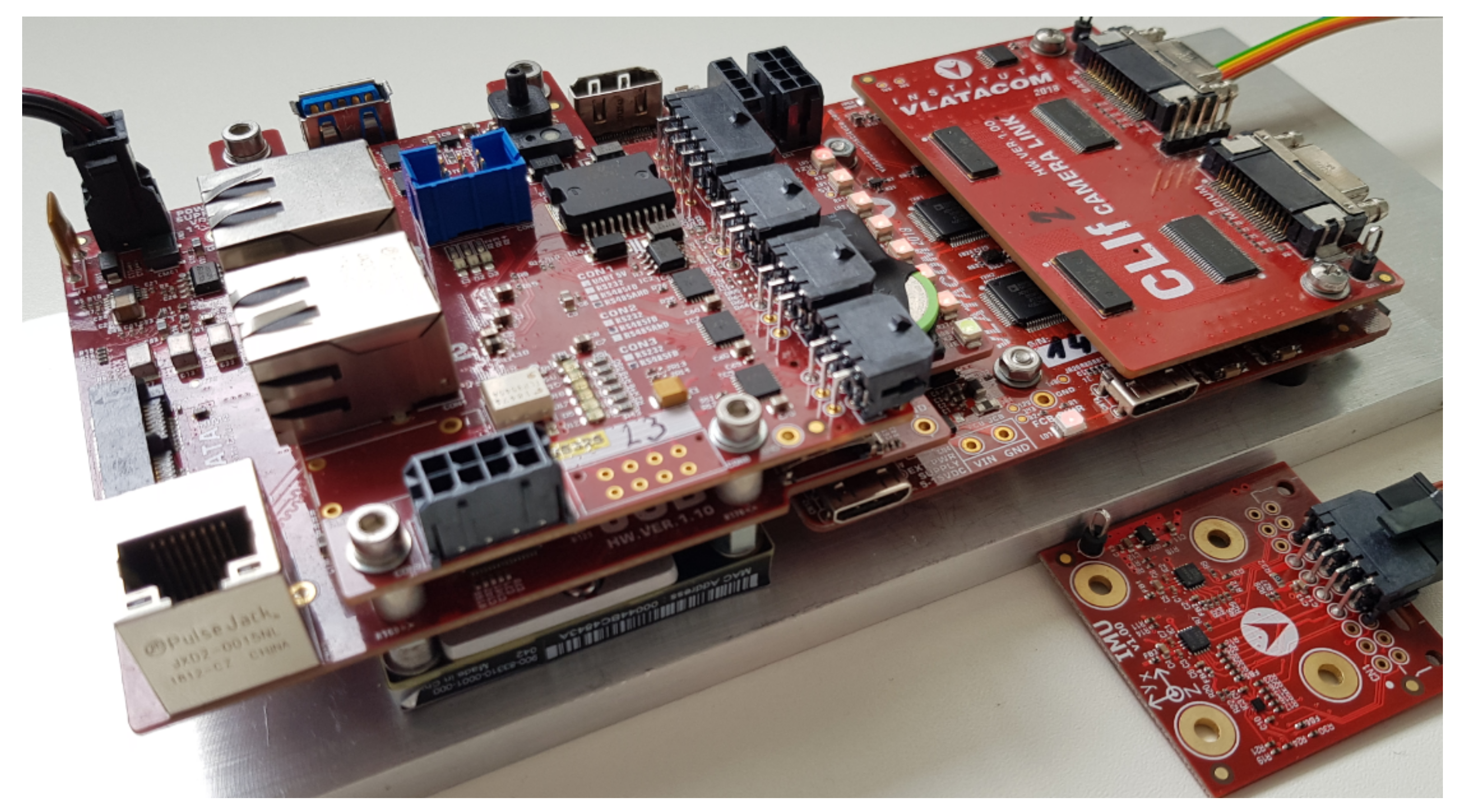
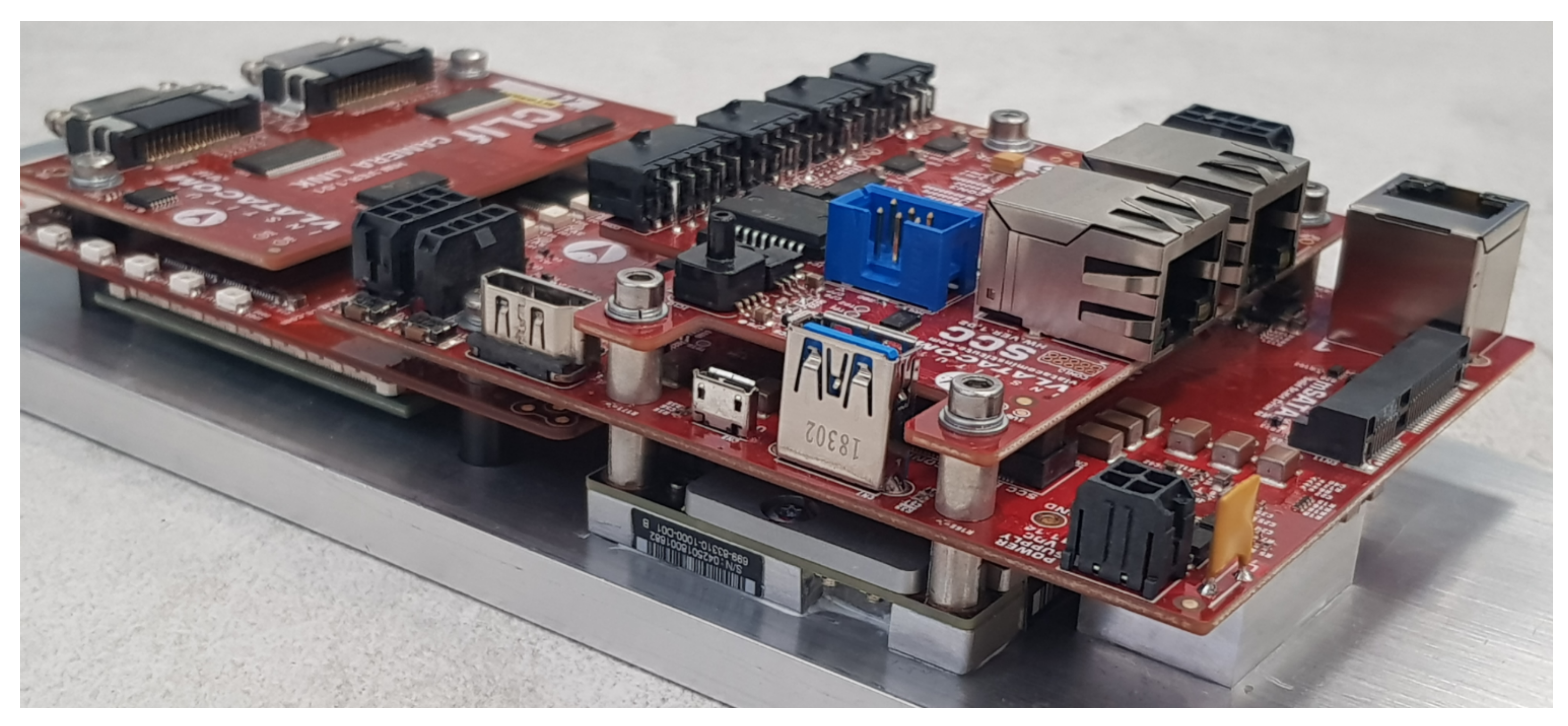
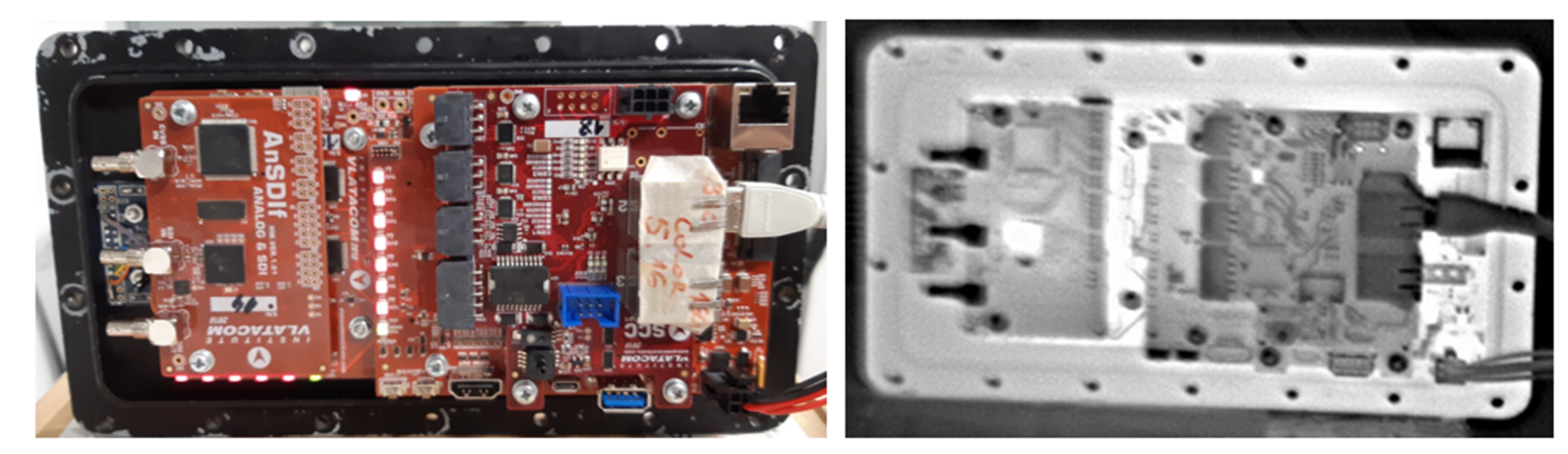
2.1. Hardware Architecture
2.2. Signal Processing
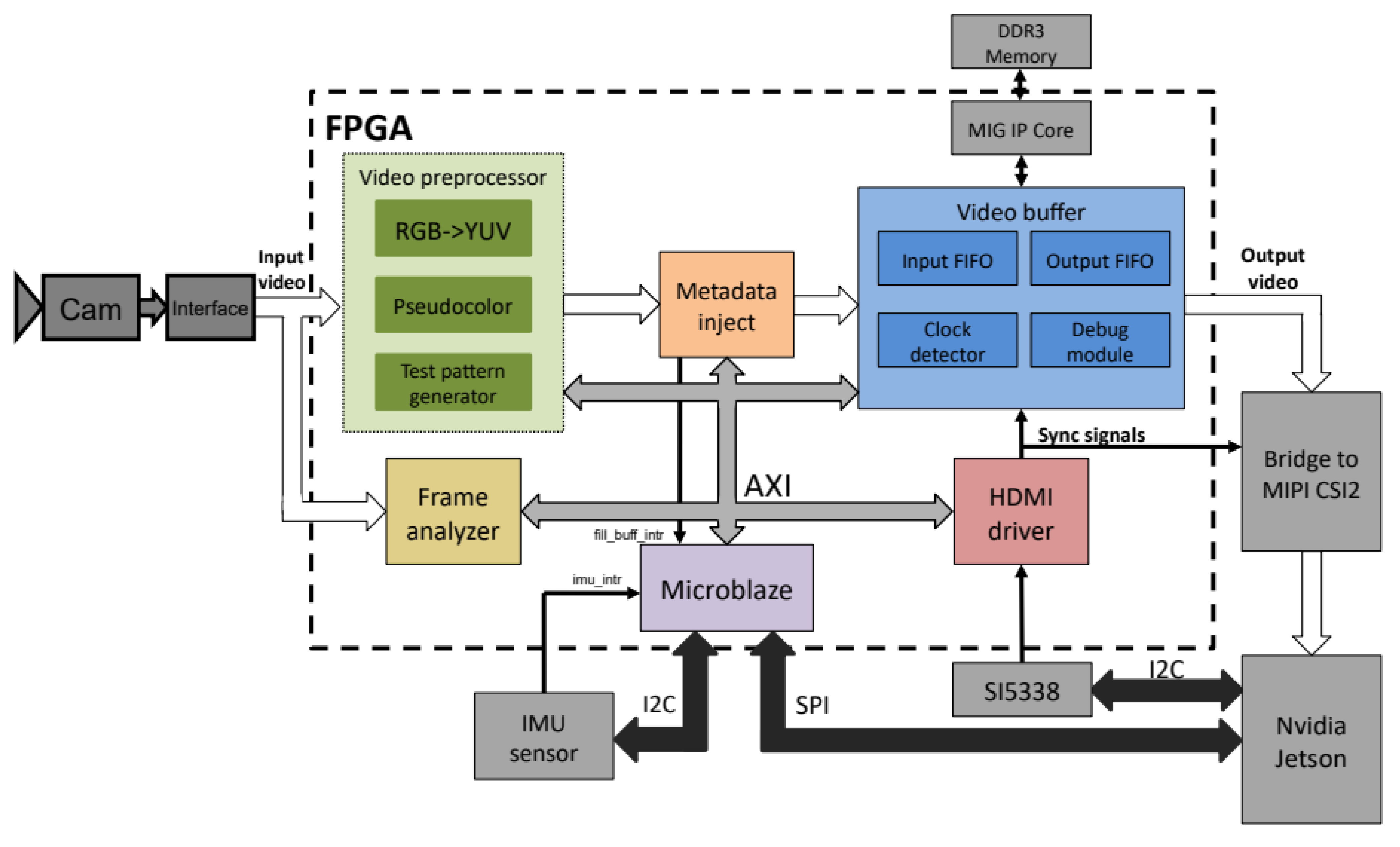
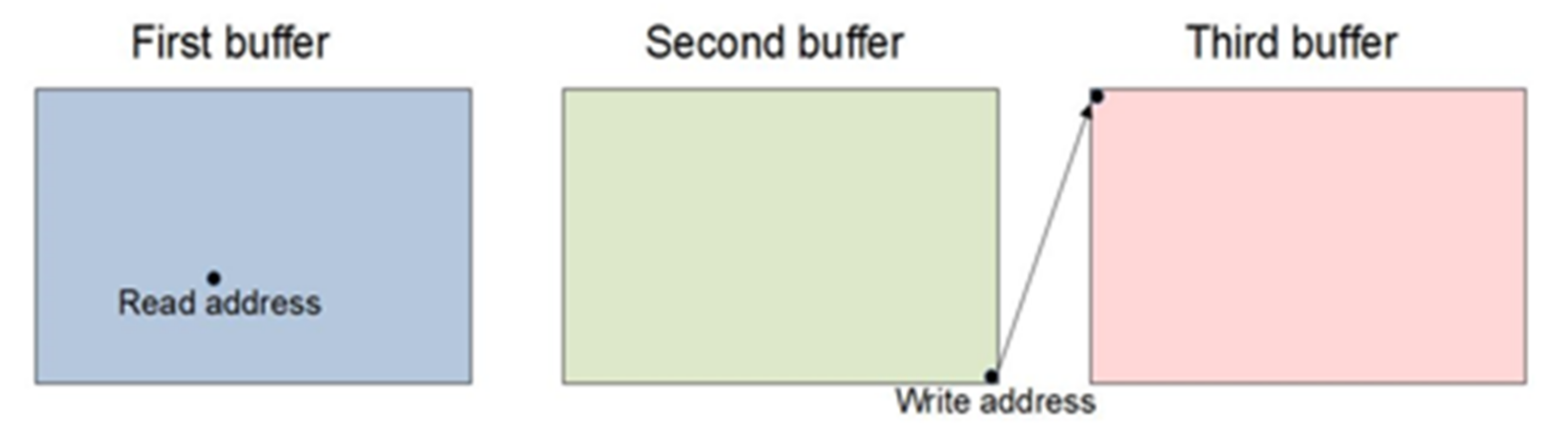
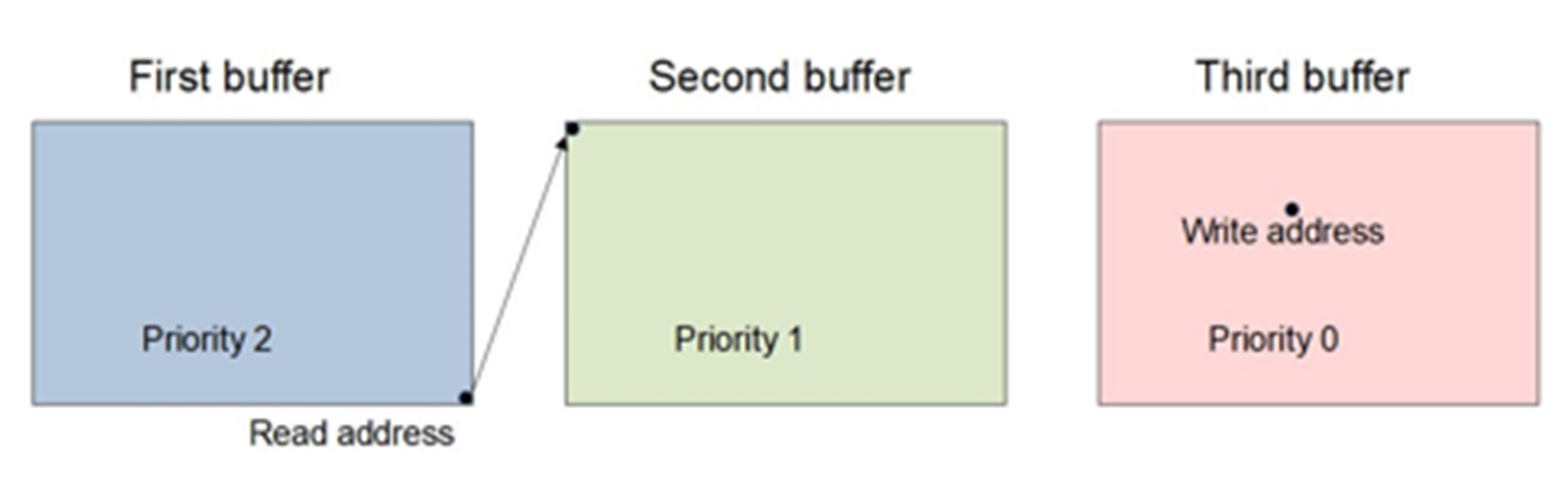
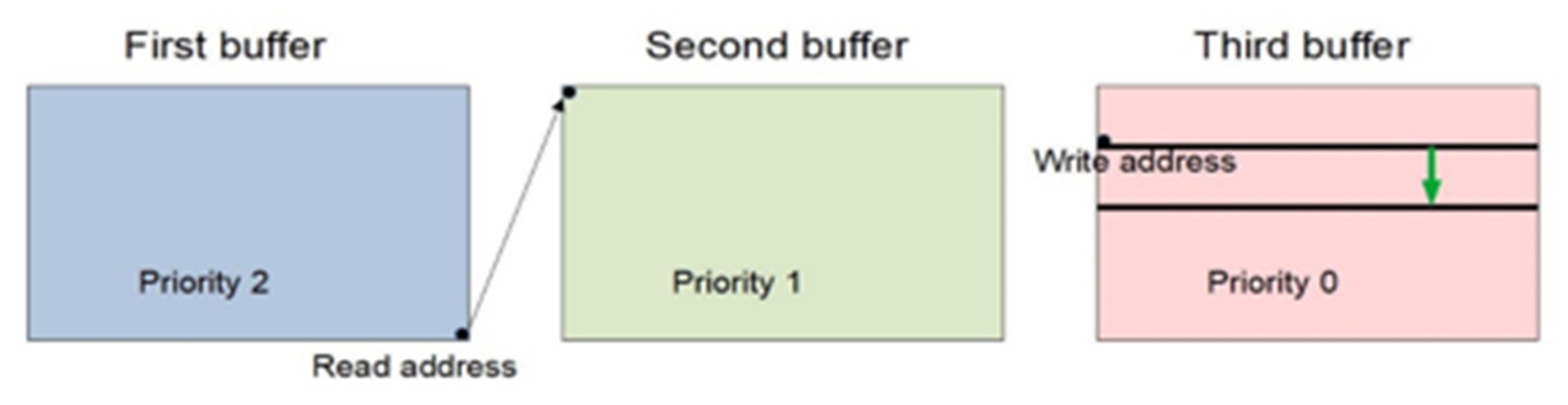
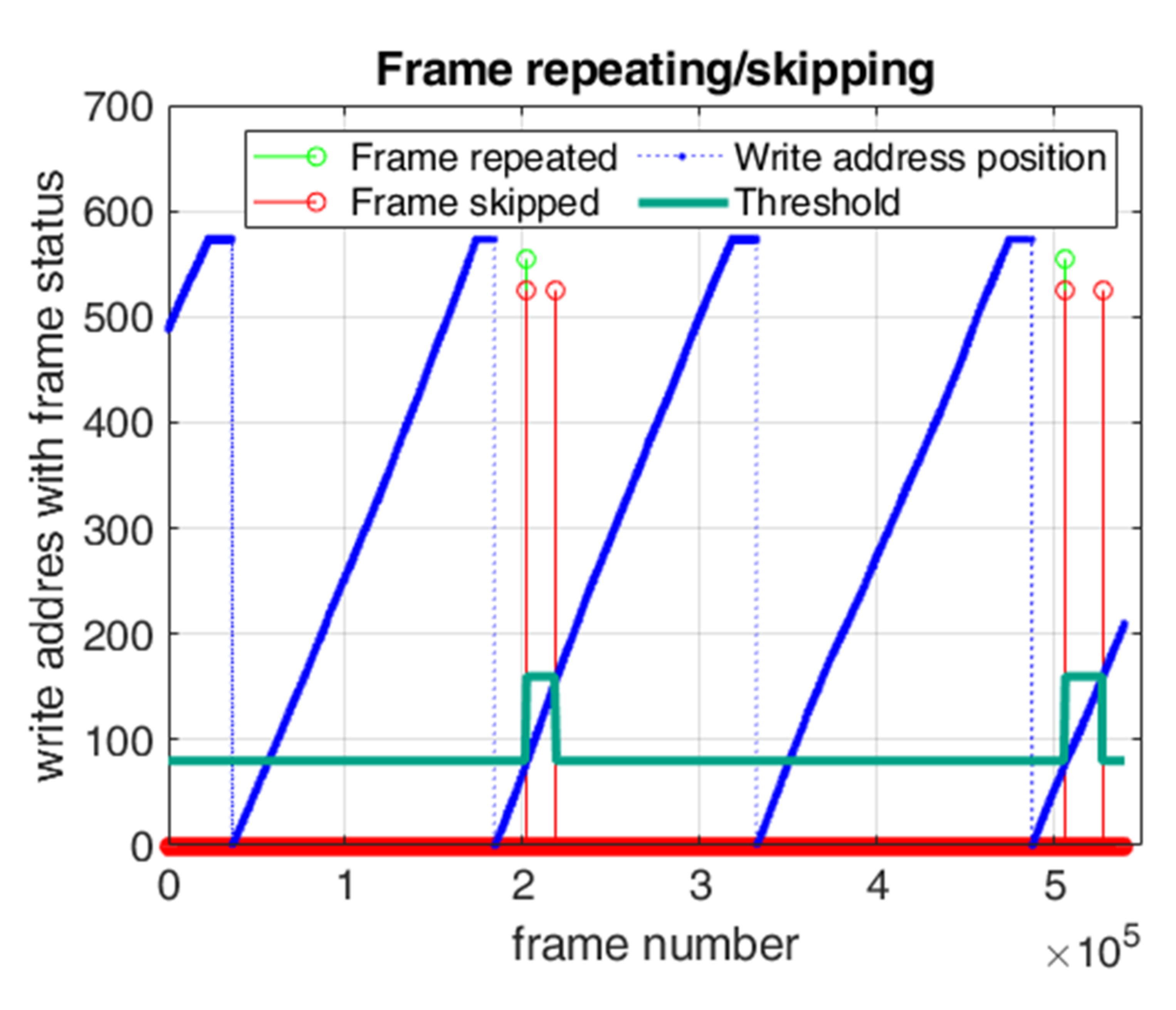
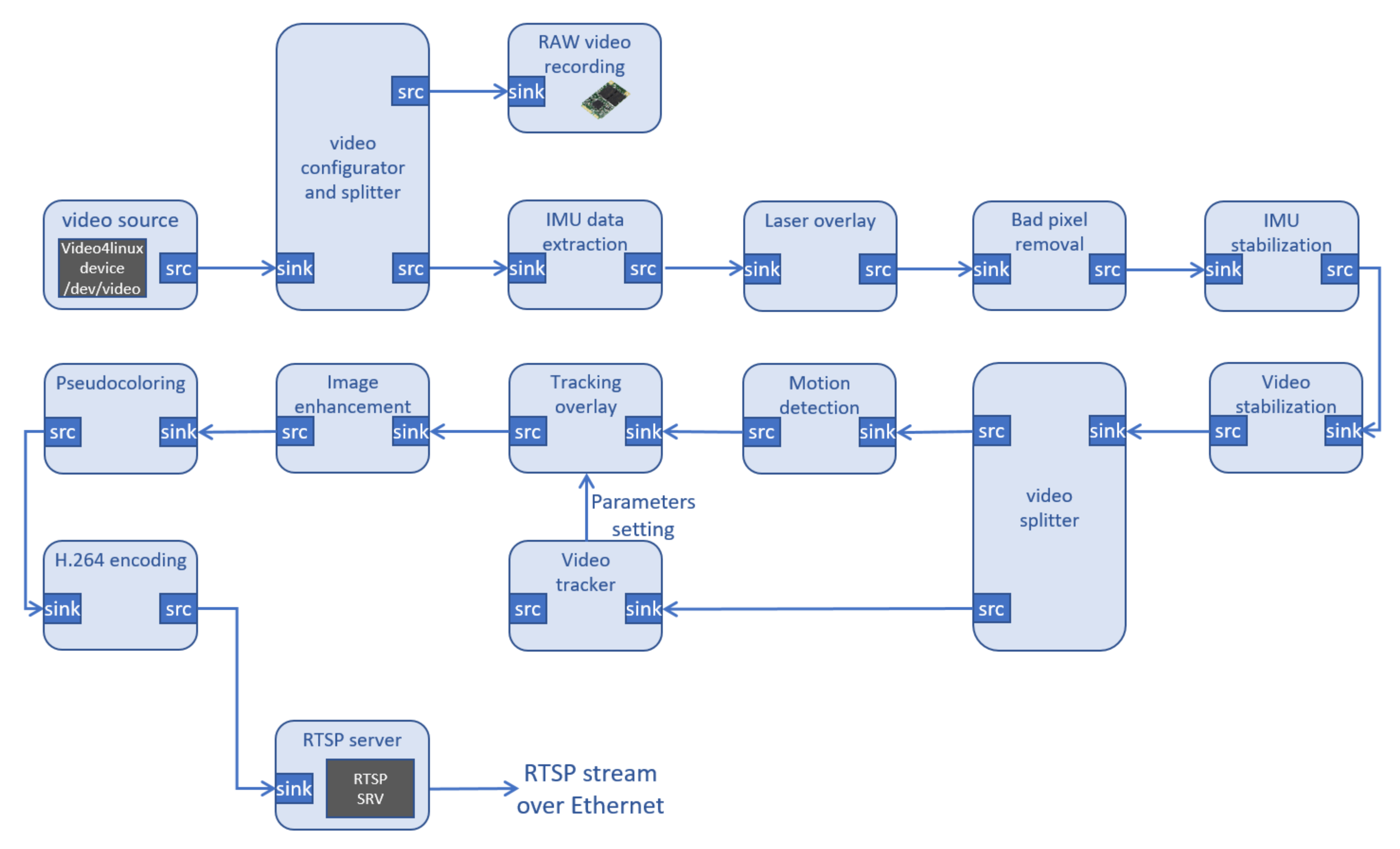
2.2.1. Video Signal Processing and Frame Buffering on FPGA Module
2.2.2. Algorithms Application—Video Signal Processing on Application Module
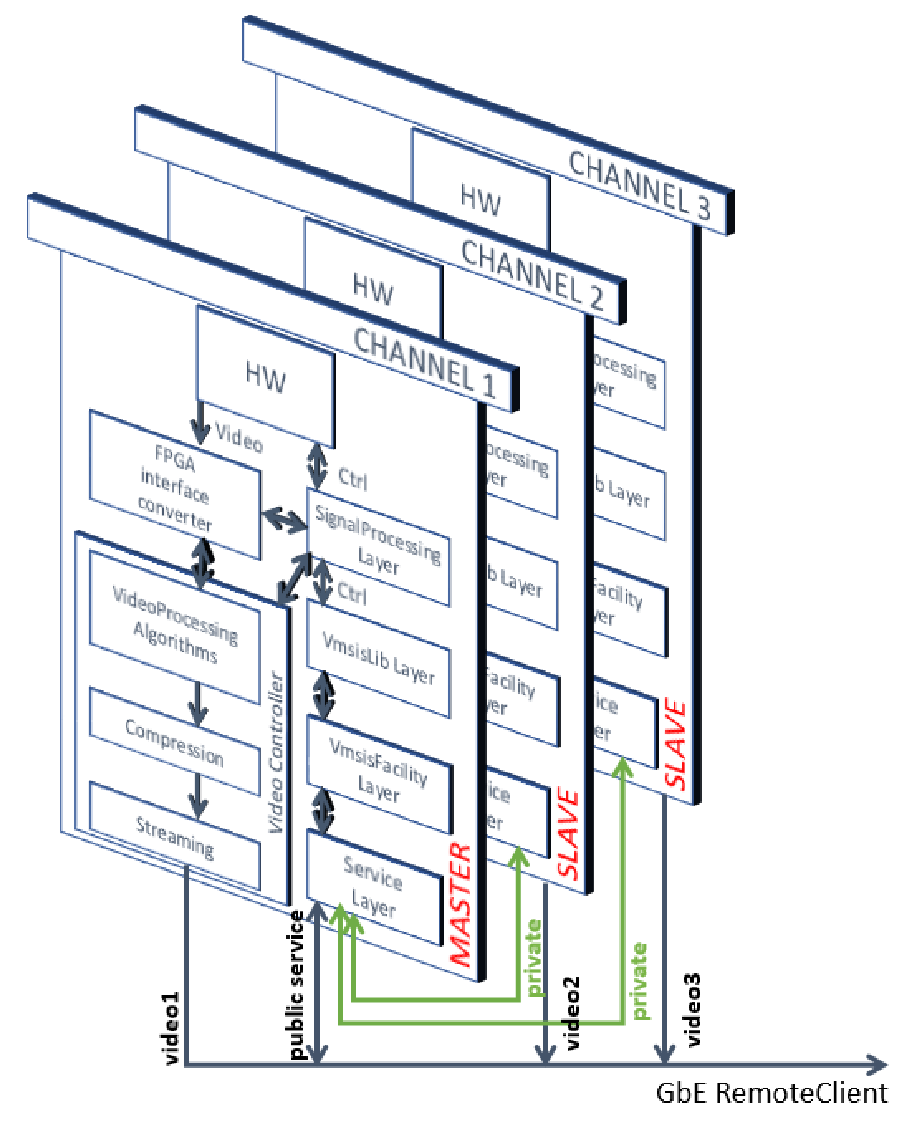
2.3. Software Architecture
- The first one is related to the acquisition, compression, processing and streaming of the video frame on the public side of the EO system;
- The second one is related to device control (camera, camera lens, tilt, etc.).
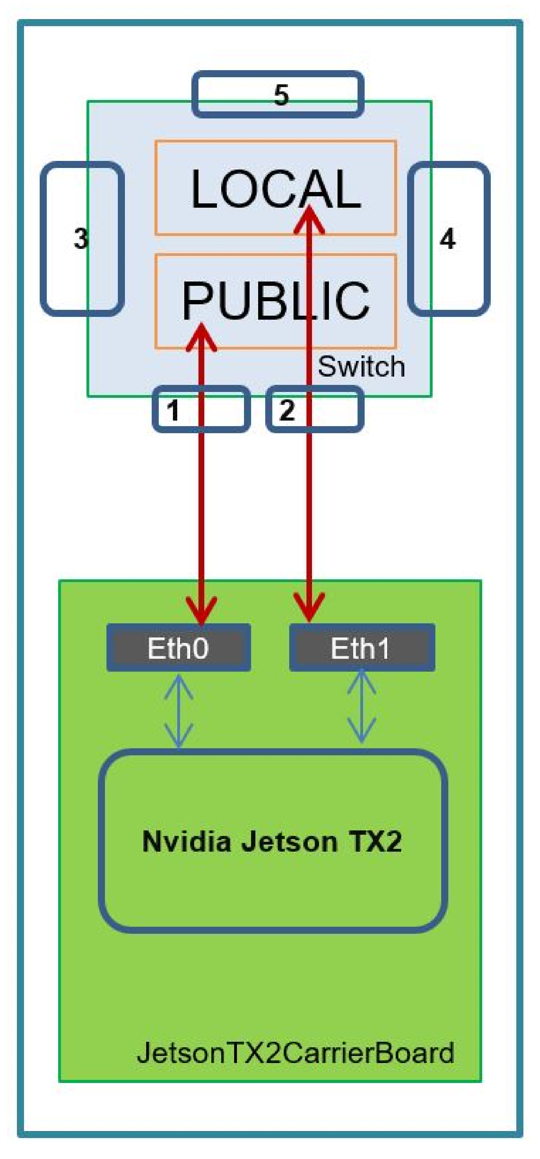
2.4. Network Architecture
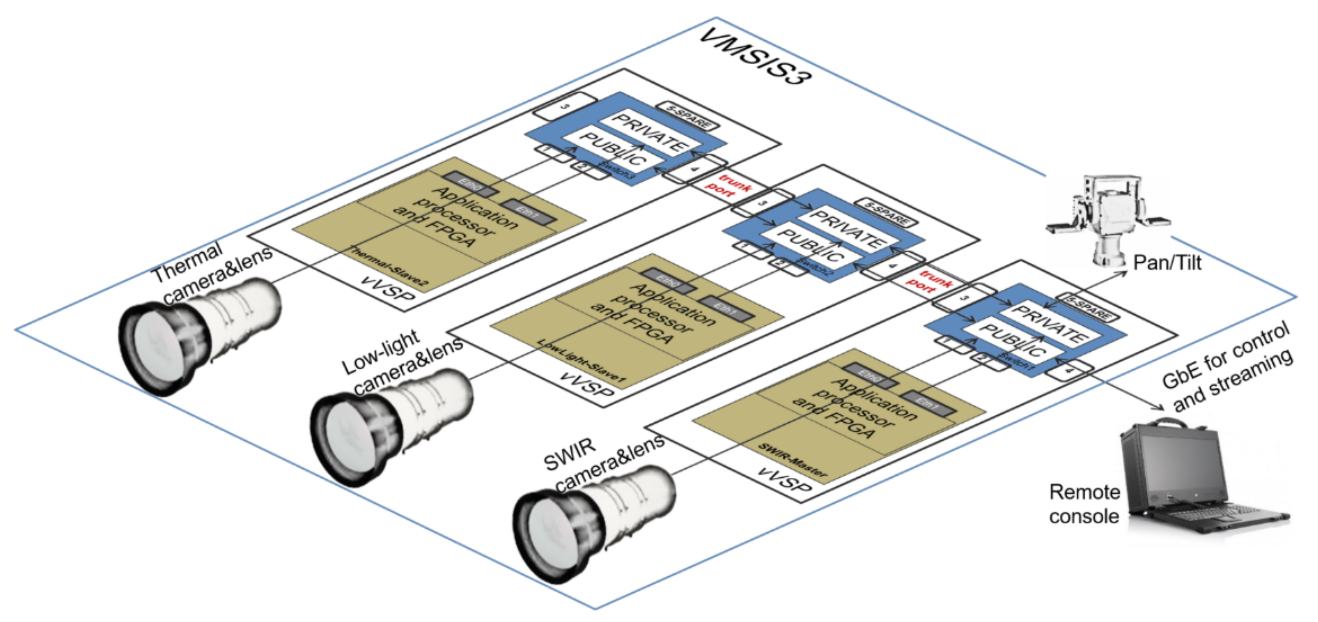
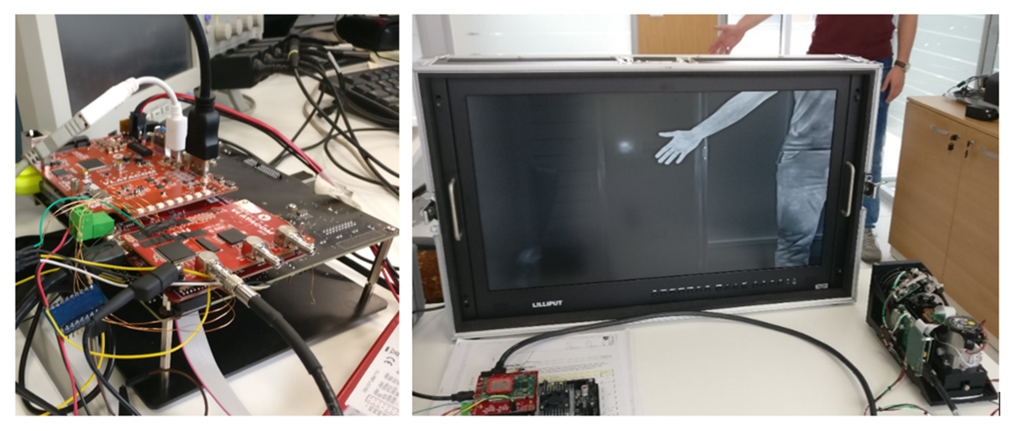
2.5. Integration
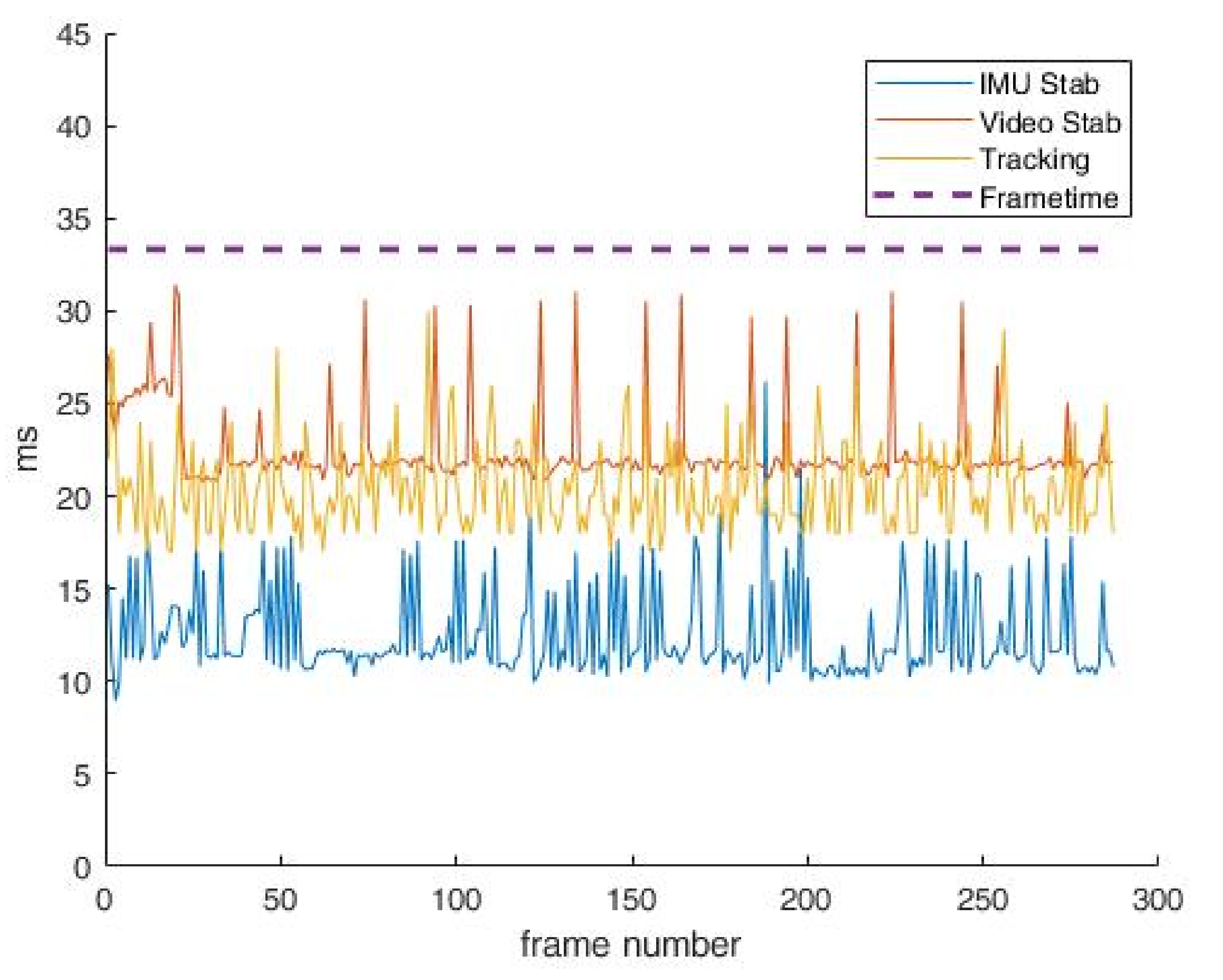
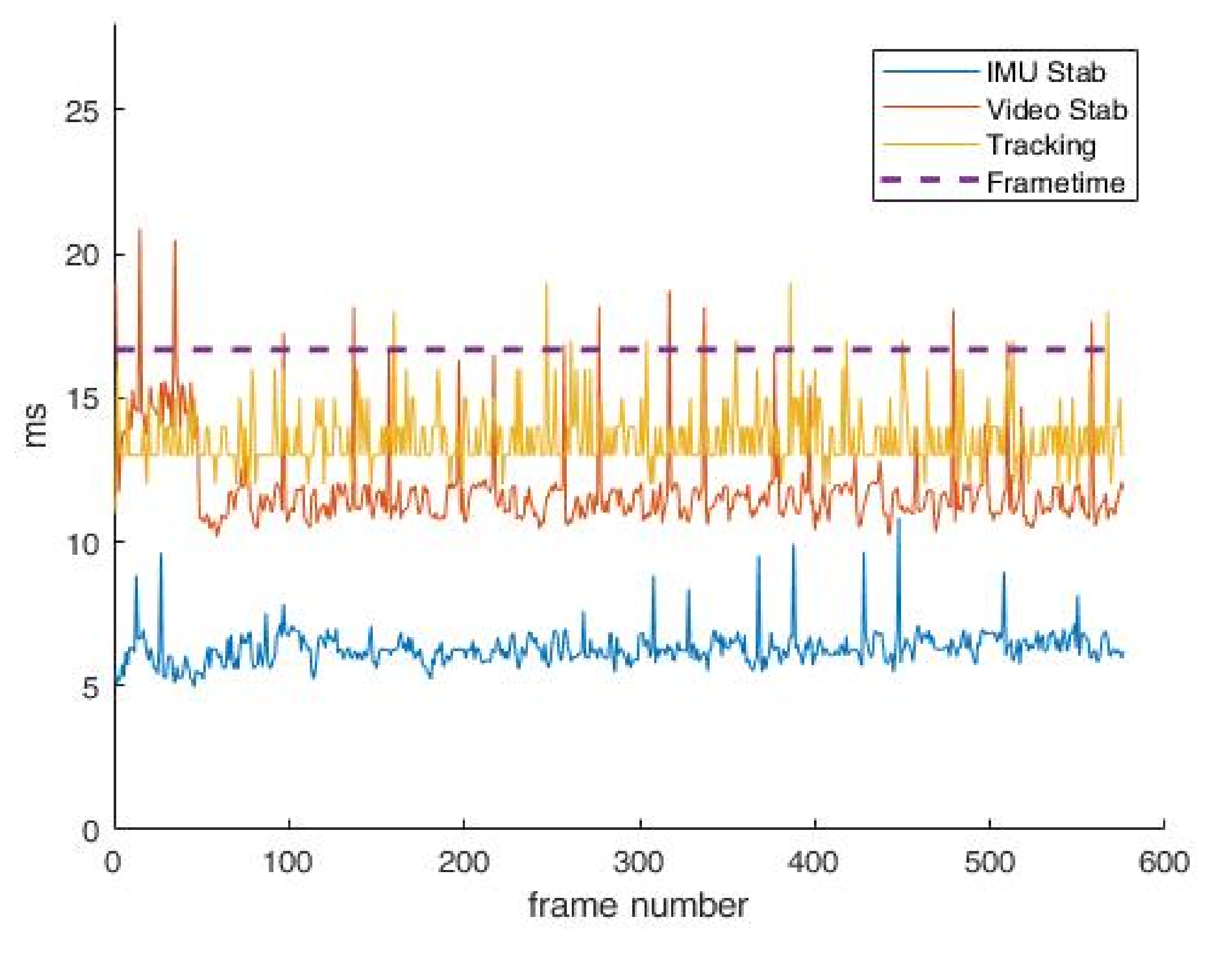
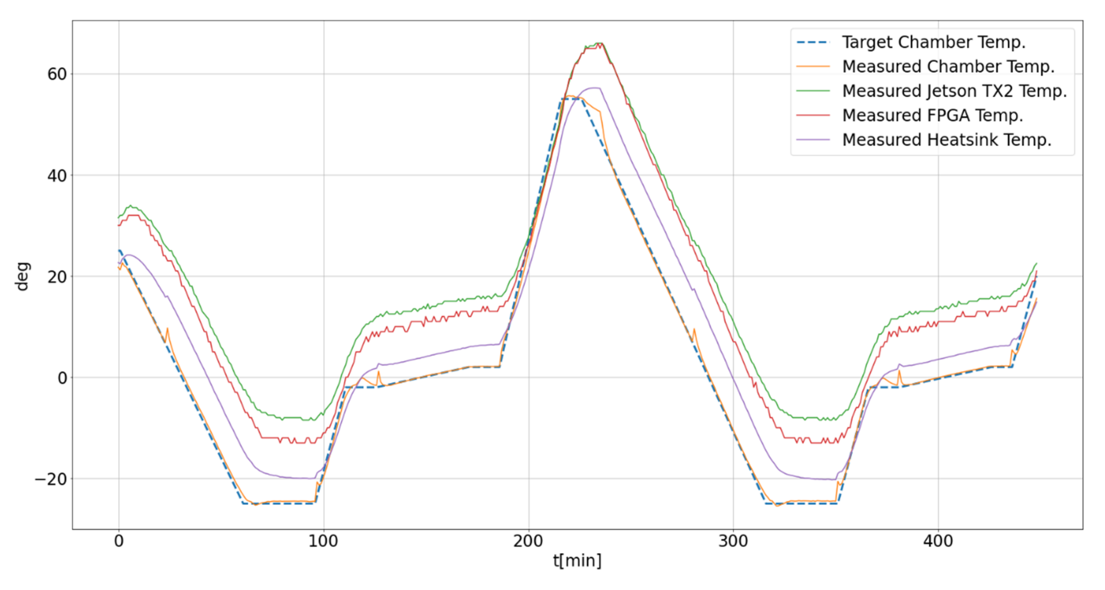
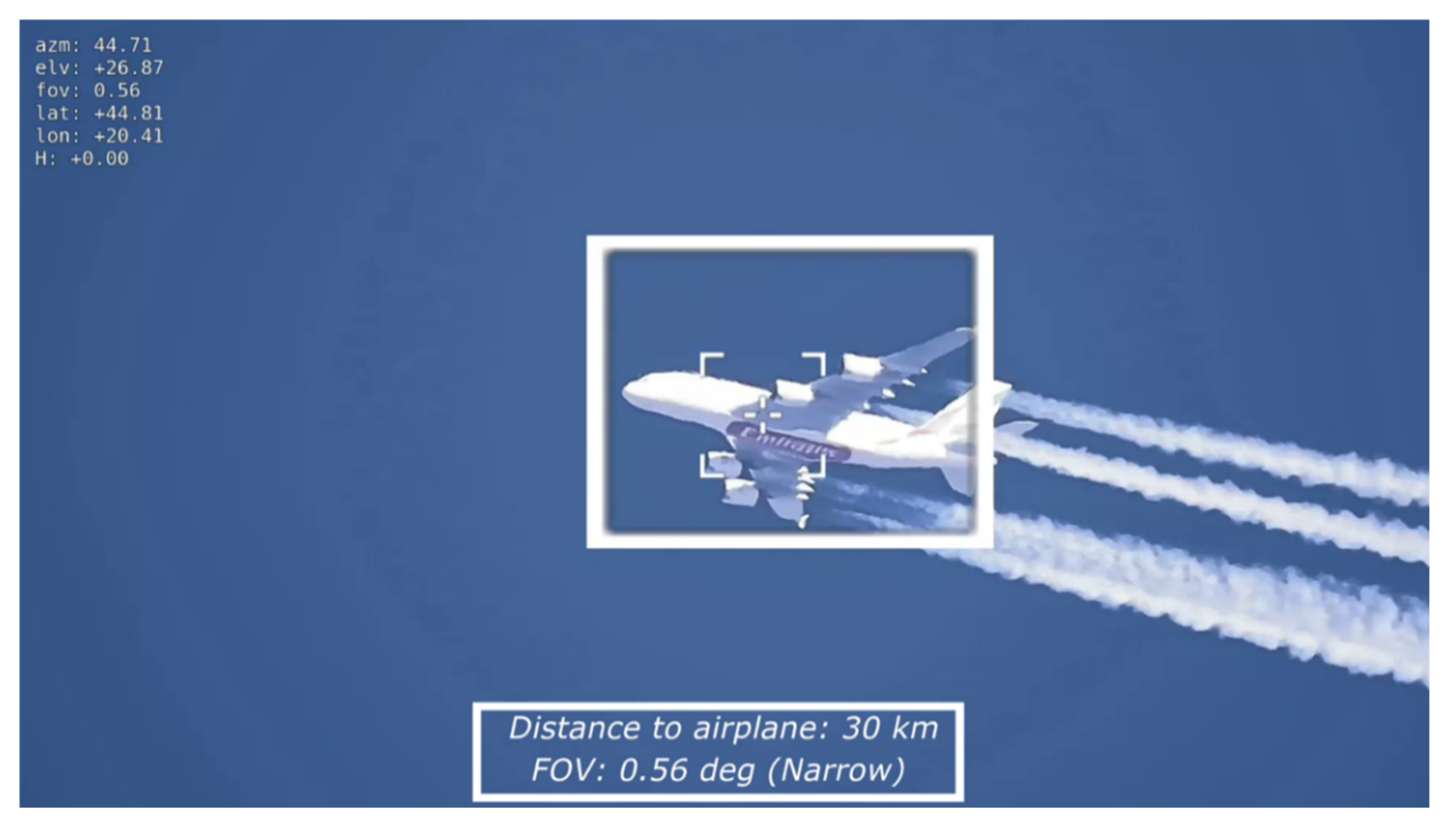
3. Results
4. Discussion
5. Conclusions
Author Contributions
Funding
Conflicts of Interest
References
- Aghajan, H.; Cavallaro, A. Multi-Camera Networks: Principles and Application; Academic Press: Cambridge, MA, USA, 2009; ISBN 9780123746337. [Google Scholar]
- Szustakowski, M.; Życzkowski, M.; Karol, M.; Kastek, M.; Dulski, R.; Szustakowski, A.M.; Bareła, J.; Markowski, P.; Kowalski, M. Ultra long range surveillance camera for critical infrastructure protection research range. In Optics and Photonics for Counterterrorism, Crime Fighting and Defence IX; and Optical Materials and Biomaterials in Security and Defence Systems Technology X, Proceedings of the SPIE Security + Defence, Dresden, Germany, 23–26 September 2013; SPIE: Bellingham, WA, USA, 2013; Volume 8901, pp. 207–213. [Google Scholar] [CrossRef]
- Kuroda, T. Essential Principles of Image Sensors; CRC Press: Boca Raton, FL, USA, 2015. [Google Scholar]
- Peric, D.; Livada, B. Analysis of SWIR Imagers Application in Electro-Optical Systems. In Proceedings of the 4th International Conference on Electrical, Electronics and Computing Engineering, IcETRAN 2017, Kladovo, Serbia, 5–8 June 2017. [Google Scholar]
- Budzier, H.; Gerlach, G. Thermal Infrared Sensors: Theory, Optimisation and Practice. In Thermal Infrared Sensors: Theory, Optimisation and Practice; John Wiley & Sons: Hoboken, NJ, USA, 2011. [Google Scholar] [CrossRef]
- Perić, D.; Livada, B.; Perić, M.; Vujić, S. Thermal Imager Range: Predictions, Expectations, and Reality. Sensors 2019, 19, 3313. [Google Scholar] [CrossRef] [PubMed] [Green Version]
- Laser Ranging Techniques by Narain Mansharamani. Available online: https://www.goodreads.com/book/show/14308867-laser-ranging-techniques (accessed on 7 December 2021).
- Göhler, B.; Lutzmann, P. Review on short-wavelength infrared laser gated-viewing at Fraunhofer IOSB. Opt. Eng. 2016, 56, 031203. [Google Scholar] [CrossRef] [Green Version]
- Slip Rings & Rotary Unions—360° Rotary Solutions—MOFLON. Available online: https://www.moflon.com/ (accessed on 6 December 2021).
- Milanović, P.D.; Popadić, I.V.; Kovačević, B.D. Gyroscope-Based Video Stabilization for Electro-Optical Long-Range Surveillance Systems. Sensors 2021, 21, 6219. [Google Scholar] [CrossRef] [PubMed]
- Stojanovic, M.; Vlahovic, N.; Stankovic, M.; Stankovic, S. Object tracking in thermal imaging using kemelized correlation filters. In Proceedings of the 2018 17th International Symposium Infoteh-Jahorina (INFOTEH), Sarajevo, Bosnia and Herzegovina, 21–23 March 2018. [Google Scholar]
- Stojanovic, B.; Puzovic, S.; Vlahovic, N.; Petrovic, R.; Stankovic, S. Real-Time Multi-Sensor Infrared Imagery Enhancement. In Proceedings of the 2018 14th Symposium on Neural Networks and Applications (NEUREL), Belgrade, Serbia, 20–21 November 2018. [Google Scholar]
- Wang, X. Intelligent multi-camera video surveillance: A review. Pattern Recognit. Lett. 2013, 34, 3–19. [Google Scholar] [CrossRef]
- Vision4ce. Vision4ce Products 2020. Available online: https://www.vision4ce.com/ (accessed on 11 December 2021).
- SightLine Homepage—SightLine Applications 2020. Available online: https://sightlineapplications.com/ (accessed on 11 December 2021).
- Desmouliers, C.; Oruklu, E.; Aslan, S.; Saniie, J.; Vallina, F.M. Image and video processing platform for field programmable gate arrays using a high-level synthesis. IET Comput. Digit. Tech. 2012, 6, 414–425. [Google Scholar] [CrossRef]
- Latinović, N.; Popadić, I.; Milanović, P.; Perić, M.; Veinović, M. Multisensor Imaging System Video Interface Implementation in FPGA. In Proceedings of the International Scientific Conference on Information Technology and Data Related Research SINTEZA 2019, Novi Sad, Serbia, 20 April 2019. [Google Scholar]
- Popadić, I.; Perić, M.; Tomić, B.; Simić, A.; Milanović, P. High-end video processing platform for electro-optical systems. In Proceedings of the Proceedings of the 9th International Scientific Conference on Defensive Technologies, Belgrade, Serbia, 15–16 October 2020; pp. 297–303. [Google Scholar]
- Jetson TX2 Module | NVIDIA Developer. Available online: https://developer.nvidia.com/embedded/jetson-tx2 (accessed on 11 December 2021).
- Xilinx 7 Series FPGAs Datasheet. 2020, pp. 1–19. Available online: https://www.xilinx.com/support/documentation/data_sheets/ds180_7Series_Overview.pdf (accessed on 11 December 2021).
- Enclustra FPGA Solutions|Mercury+ KX2|Xilinx Kintex-7 FPGA Module|XC7K160T|XC7K325T|XC7K410T. Available online: https://www.enclustra.com/en/products/fpga-modules/mercury-kx2/ (accessed on 11 December 2021).
- Xilinx Zynq UltraScale + MPSoC Data Sheet: Overview. 2019. Available online: https://www.xilinx.com/support/documentation/data_sheets/ds891-zynq-ultrascale-plus-overview.pdf (accessed on 11 December 2021).
- SMPTE ST 292-1:2012; SMPTE Standard—1.5 Gb/s Signal/Data Serial Interface. Society of Motion Picture and Television Engineers: New York, NY, USA, 2012.
- AIA. Specifications of the Camera Link Interface Standard for Digital Cameras and Frame Grabbers; Version 2.0; AIA: Ann Arbor, MI, USA, 2012. [Google Scholar]
- ITU Recommendation Interface for Digital Component Video Signals in 525-Line and 625-Line Television Systems Operating at the 4:2:2 Level of Recommendation ITU-R BT.601; ITU-R BT.656-5 (12/2007); BT Series Broadcasting Service (Television): Geneva, Switzerland, 2011; Available online: https://www.itu.int/rec/R-REC-BT.656/en (accessed on 11 December 2021).
- Popadić, I.; Todorović, B.M.; Reljin, I. Method for HDR-like imaging using industrial digital cameras. Multimed. Tools Appl. 2017, 76, 12801–12817. [Google Scholar] [CrossRef]
- MIPI Camera Serial Interface 2 (MIPI CSI-2). Available online: https://www.mipi.org/specifications/csi-2 (accessed on 11 December 2021).
- Video4Linux Devices—The Linux Kernel Documentation. Available online: https://www.kernel.org/doc/html/v4.9/media/v4l-drivers/index.html (accessed on 11 December 2021).
- Memory Interface. Available online: https://www.xilinx.com/products/intellectual-property/mig.html (accessed on 11 December 2021).
- Greisen, P.; Heinzle, S.; Gross, M.; Burg, A.P. An FPGA-based processing pipeline for high-definition stereo video. EURASIP J. Image Video Process. 2011, 18. [Google Scholar] [CrossRef] [Green Version]
- Williams, J.; Mikhelson, I. Triple frame buffer FPGA implementation. HardwareX 2019, 5, e00064. [Google Scholar] [CrossRef]
- GStreamer: Open Source Multimedia Framework. Available online: https://gstreamer.freedesktop.org/ (accessed on 11 December 2021).
- Pavlović, M.; Vlahović, N.; Perić, M.; Simić, A.; Stanković, S. Real-Time Dead Pixels Removal in Thermal Imaging. In Proceedings of the 6th IcETRAN, Srebrno Jezero, Serbia, 3–6 June 2019; pp. 345–348. [Google Scholar]
- Rfc2326. Available online: https://datatracker.ietf.org/doc/html/rfc2326 (accessed on 11 October 2021).
- Profile S—ONVIF. Available online: https://www.onvif.org/wp-content/uploads/2017/01/ONVIF_Profile_-S_Specification_v1-1-1.pdf (accessed on 11 December 2021).
- Standard, G. GenICam GenTL Standard. 2015. Available online: https://www.emva.org/wp-content/uploads/GenICam_Standard_v2_1_1.pdf (accessed on 11 December 2021).
- GenICam—EMVA. Available online: https://www.emva.org/wp-content/uploads/GenICam_Standard_v2_0.pdf (accessed on 11 December 2021).
- Hartpence, B. Pocket Guide to Routing and Switching; Wallace, S., Hendrickson, M., Eds.; O’Reilly Media: Sebastopol, CA, USA, 2011; ISBN 9781449306557. [Google Scholar]
- Cizelj, V. Vlatacom Institute of High Technology—Ten Years since the First Accreditation; Vlatacom Institute: Belgrade, Serbia, 2021; ISBN 978-86-7466-891-7. [Google Scholar]
- Jetson Product Lifecycle | NVIDIA Developer. Available online: https://developer.nvidia.com/embedded/community/lifecycle (accessed on 11 October 2021).
- Dimitrievski, M.; Van Hamme, D.; Veelaert, P.; Philips, W. Cooperative Multi-Sensor Tracking of Vulnerable Road Users in the Presence of Missing Detections. Sensors 2020, 20, 4817. [Google Scholar] [CrossRef] [PubMed]
- Jahromi, B.S.; Tulabandhula, T.; Cetin, S. Real-Time Hybrid Multi-Sensor Fusion Framework for Perception in Autonomous Vehicles. Sensors 2019, 19, 4357. [Google Scholar] [CrossRef] [PubMed] [Green Version]


| Buffering Technique | Latency | Behavior |
|---|---|---|
| Single buffering | Part of frame | Low latency/sync problem |
| Double buffering | 0  1 frame 1 frame | Low latency/sync problem |
| Triple buffering | 1 2 frames | Higher latency/no sync problem |
| Modified triple buffering | Limit 1 frame + limit | Medium latency/no sync problem |
| Task | Traditional Approach | VVSP Concept | Contribution |
|---|---|---|---|
| Video signal monitoring | Analogue PAL or NTSC digital (HD) SDI or CoaxPress. | Digitalized H264. | Easier interfacing to command control systems. No need for additional hardware/software. |
| Camera interfacing | PAL/NTSC—easy (HD)SDI/CoaxPress—easy, limited range CameraLink or LVDS—difficult, converter to HD-SDI needed introduced latency and possible format change. | Easy connection to any interface on camera with just choosing proper interface board. This is important for thermal and SWIR cameras, which predominantly utilize CameraLink or LVDS interface for maximal performance. | Interfacing to any camera interface is direct without any resolution change or additional latency. |
| Pan-tilt control | Via Pelco-D, ONVIF or similar protocol. | Via ONVIF protocol. For a critical algorithm such as target tracking, pan-tilt drive is direct from the VVSP without any additional latency. | VVSP has an advantage in applications executed directly on HW- and AI-based control. |
| Pan-tilt positioner slip ring communication | Limited to coaxial or Ethernet interfaces; otherwise, converters are needed. Additional interface is needed for pan-tilt, LRF and lenses control. | Only uses one Ethernet interface for both video streaming, camera, lenses, LRF and pan tilt control. | Reduces requirements for pan-tilt positioner slip ring. |
| Fanless operation | Some processor modules may require additional cooling. | VVSP is completely passively cooled. | Efficient system cooling which is tested even in desert conditions. |
| Resolution | Limited to PAL or NTSC. High-resolution/dynamic-range imaging not supported. Digital interfaces have no limitations. | Full HD resolution and high dynamic range that is critical for, e.g., thermal imaging, which is fully supported. | Much better image quality. |
| Latency | Minimal latency before external compressing hardware is used. | About 300 ms. Please note that critical algorithms (e.g., tracking) are executed on vVSP, without any latency. | If an MSEOS is integrated into the C2 system, there are no differences. |
| Target tracking | Executes on external hardware that controls pan-tilt. For good performance, the controller should be installed close to the MSEOS. | Executes on VVSP. Utilizes full resolution and frame rate of all sensors. No additional latency. Very compact solution. | Considerable advantage for VVSP due to direct sensor access. |
| Image stabilization | Limited to image-based algorithms. Depends on the particular scene. | Can utilize different methods (e.g., IMU stabilization [10]). | Much more flexibility than the traditional approach. |
| Image fusion from multiple cameras (e.g., thermal and visible) | External hardware. Time synchronization and image registration might be difficult to calibrate. | A dedicated VVSP module can run image fusion algorithm acting as a “virtual video channel”. | More flexibility and easier calibration. |
| AI target recognition | Need to digitize the image prior to the application of AI modules. The concept limits resolution, which reflects on AI-based solution performance. | Full resolution of the image can be utilized for AI-based target detection application. In cases of a lack of computational power, additional VVSP modules can be added. | Much more flexibility, especially if target detection is linked to target tracking with pan-tilt movement in order to keep a tracked target in the center of the scene. |
| Image enhancement | No possibilities. | Easy implementation of various image enhancement algorithms. | Especially important for thermal imaging. |
| Laser range finder (LRF) application | External command for measurements. Targeting reticle is very hard to implement in continuous zoom cameras. | Simple implementation of targeting reticle even in continuous zoom systems [6]. | Easier integration. Additionally, it enables the implementation of complex applications (e.g., LRF-aided target-in-lock indication for tracking systems). |
| Overall moving payload weight | Minimal or no extra payload. | Each VVSP module adds about 0.45 kg in weight. | This is a small drawback since the weight of cameras and lenses in long-range MSEOS is much bigger. |
| Private network for Ethernet devices | Additional manageable GbE switch is required. | A manageable GbE switch is integrated in the VVSP module. | VLANs configuration enabled. Important devices connected to the network can be hidden from the outside world. |
| Command–control (C2) system interfacing | Requires protocol conversion box for video digitizing and range extension. | Everything needed for C2 system integration is obtained via a single Ethernet port. | Easier interfacing to the C2 system. |
| System scalability (adding a new camera to the system) | System is limited to a certain number of cameras or requires additional hardware and/or system architecture redesign. | Only an additional VVSP is required. This module is connected to the existing system network over GbE. | This is made possible by the initial concept of distributed system architecture. |
Publisher’s Note: MDPI stays neutral with regard to jurisdictional claims in published maps and institutional affiliations. |
© 2022 by the authors. Licensee MDPI, Basel, Switzerland. This article is an open access article distributed under the terms and conditions of the Creative Commons Attribution (CC BY) license (https://creativecommons.org/licenses/by/4.0/).
Share and Cite
Latinović, N.; Popadić, I.; Tomić, B.; Simić, A.; Milanović, P.; Nijemčević, S.; Perić, M.; Veinović, M. Signal Processing Platform for Long-Range Multi-Spectral Electro-Optical Systems. Sensors 2022, 22, 1294. https://doi.org/10.3390/s22031294
Latinović N, Popadić I, Tomić B, Simić A, Milanović P, Nijemčević S, Perić M, Veinović M. Signal Processing Platform for Long-Range Multi-Spectral Electro-Optical Systems. Sensors. 2022; 22(3):1294. https://doi.org/10.3390/s22031294
Chicago/Turabian StyleLatinović, Nikola, Ilija Popadić, Branko Tomić, Aleksandar Simić, Petar Milanović, Srećko Nijemčević, Miroslav Perić, and Mladen Veinović. 2022. "Signal Processing Platform for Long-Range Multi-Spectral Electro-Optical Systems" Sensors 22, no. 3: 1294. https://doi.org/10.3390/s22031294
APA StyleLatinović, N., Popadić, I., Tomić, B., Simić, A., Milanović, P., Nijemčević, S., Perić, M., & Veinović, M. (2022). Signal Processing Platform for Long-Range Multi-Spectral Electro-Optical Systems. Sensors, 22(3), 1294. https://doi.org/10.3390/s22031294