
Development of a Reliable High-Performance WLP for a SAW Device


Abstract
:1. Introduction
1.1. Historical View of SAW Device Package
1.2. SAW Device Package Design
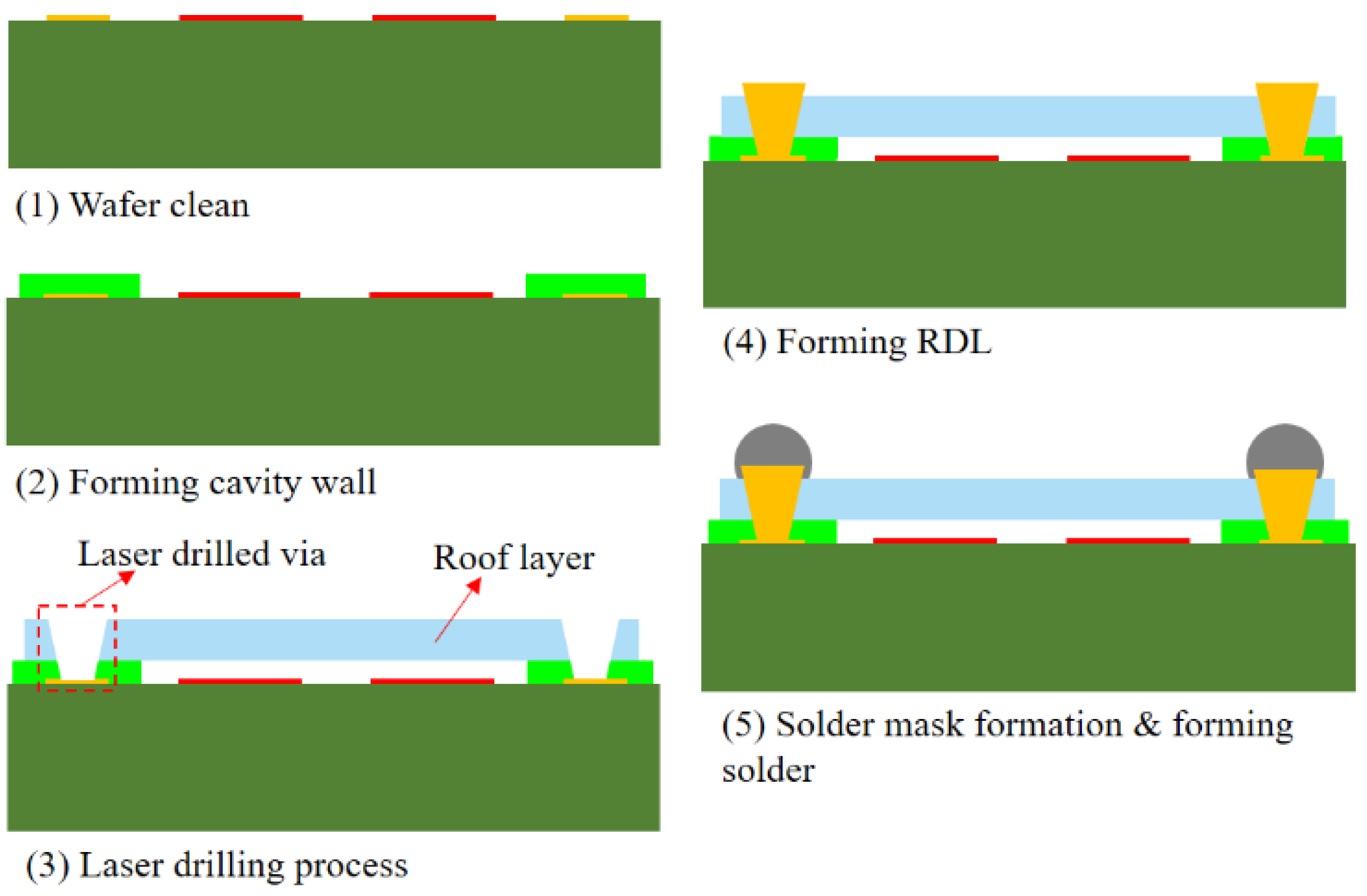
2. Process Flow of the SAW Device’s WLP and the Typical Failure Mode
2.1. Process Flow of SAW Device WLP
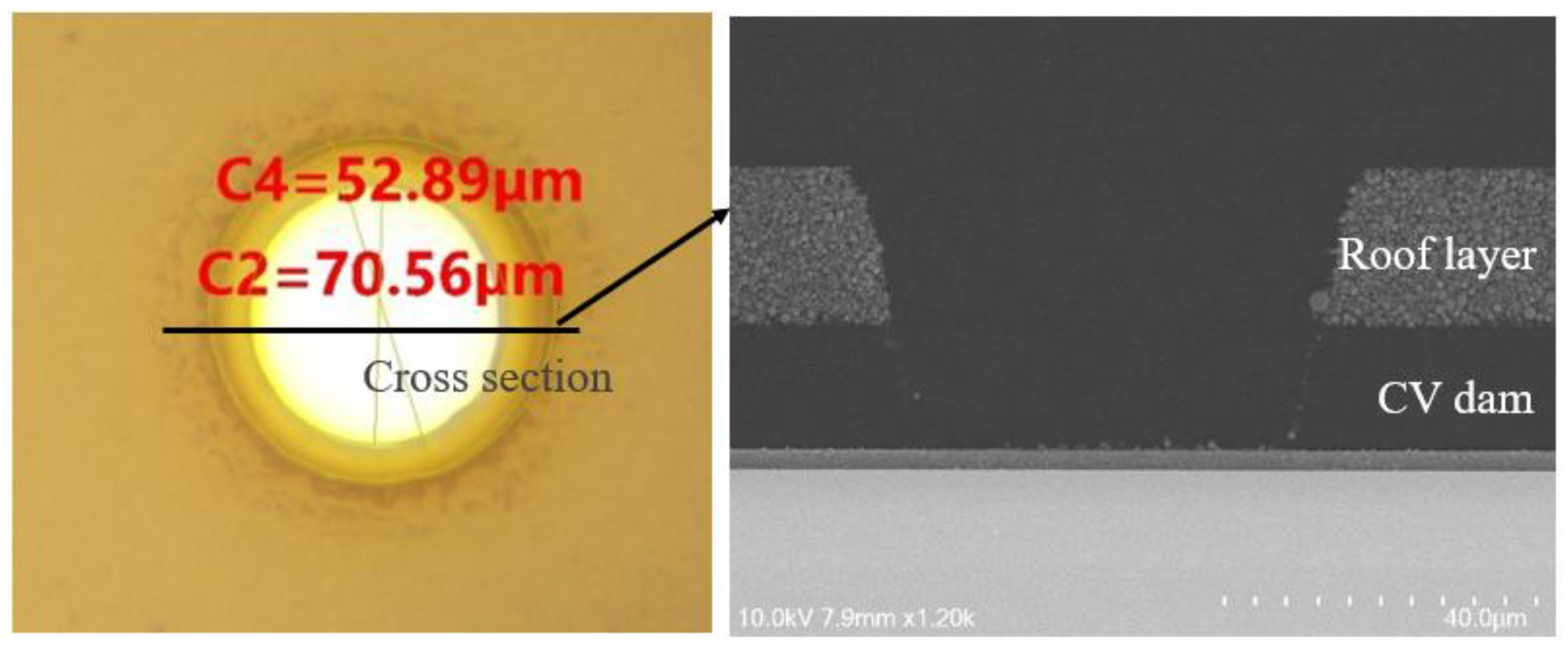
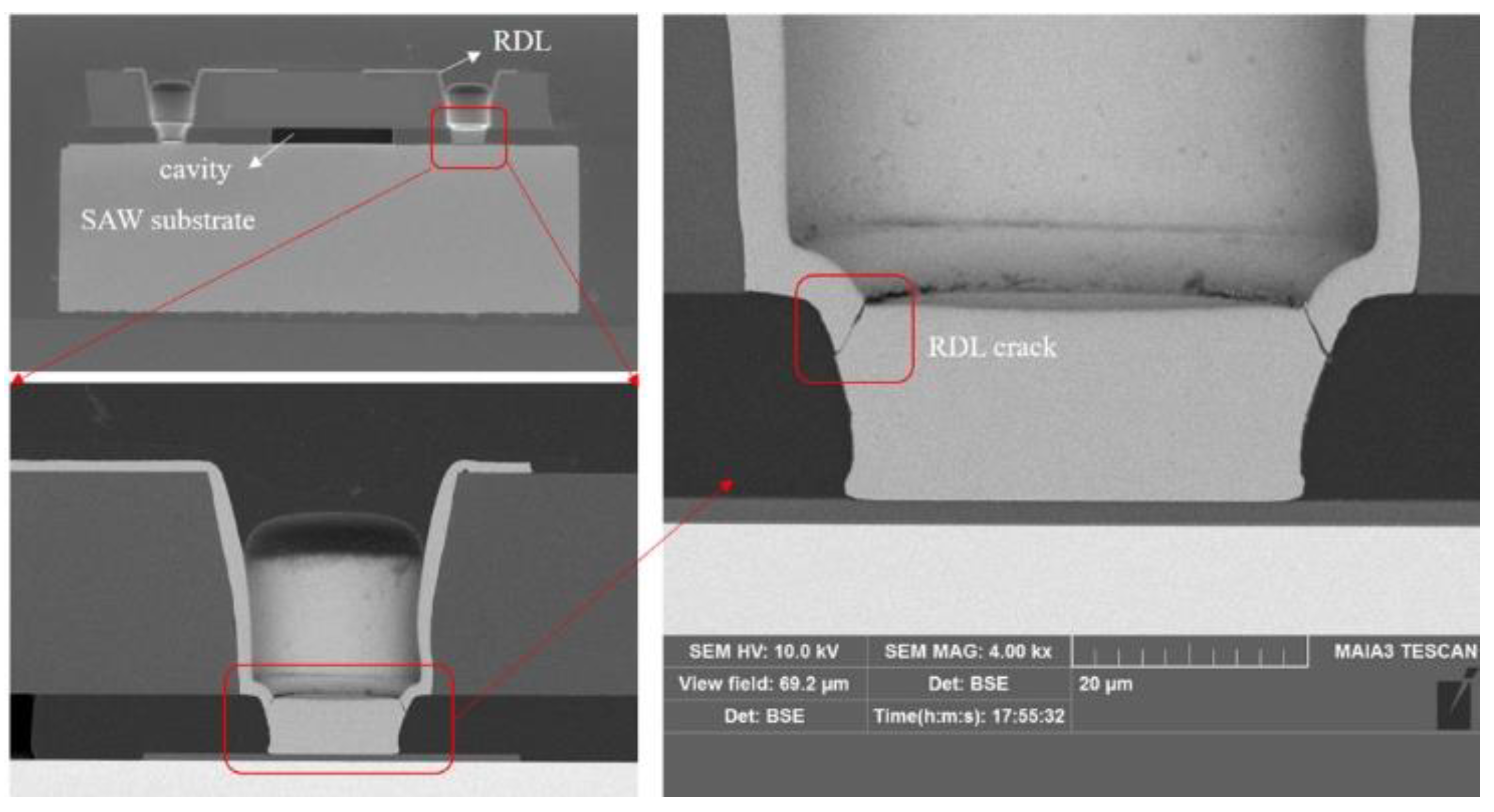
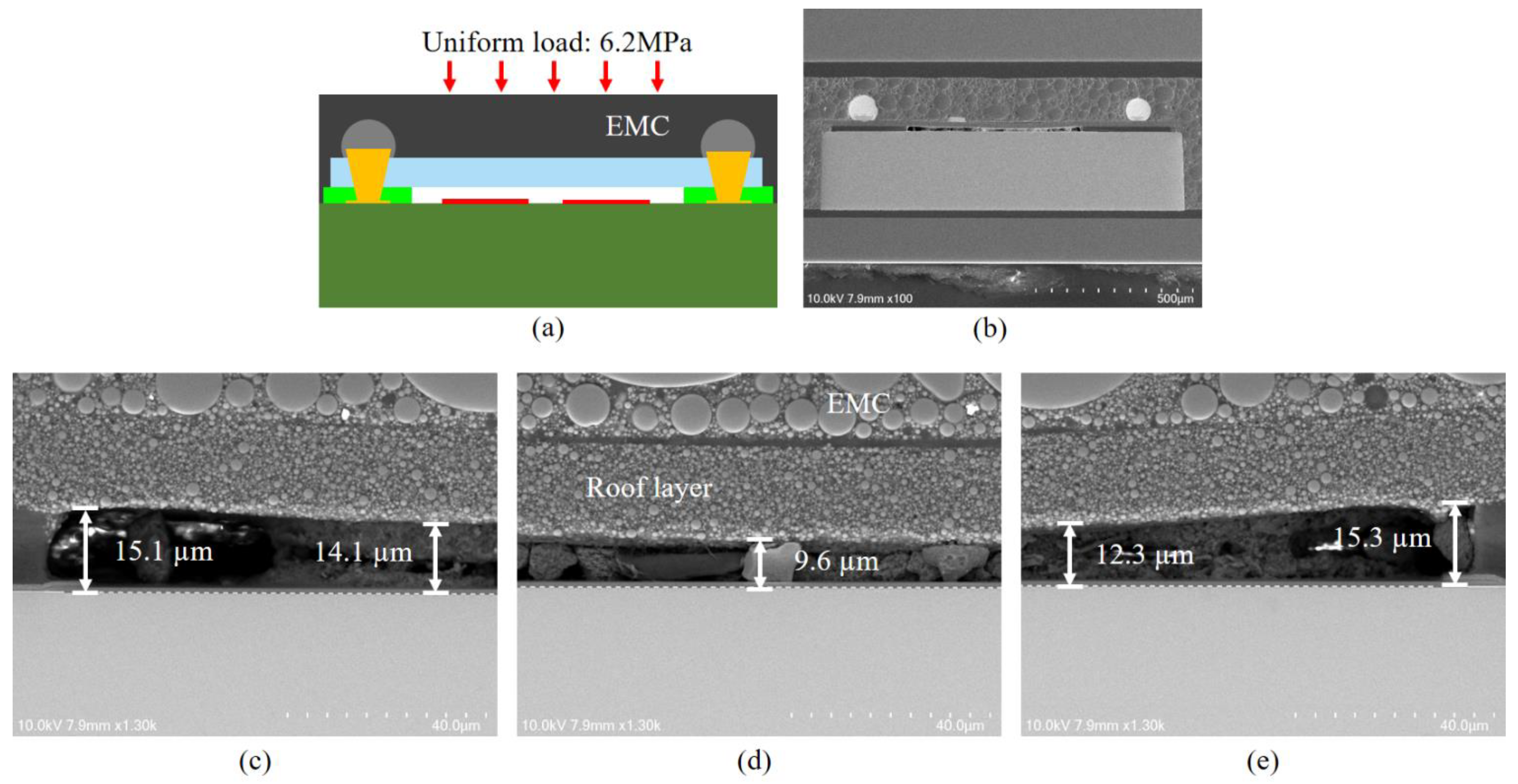
2.2. The Experimental Results of Typical Failure Mode
3. FE Model of a SAW Filter’s WLP
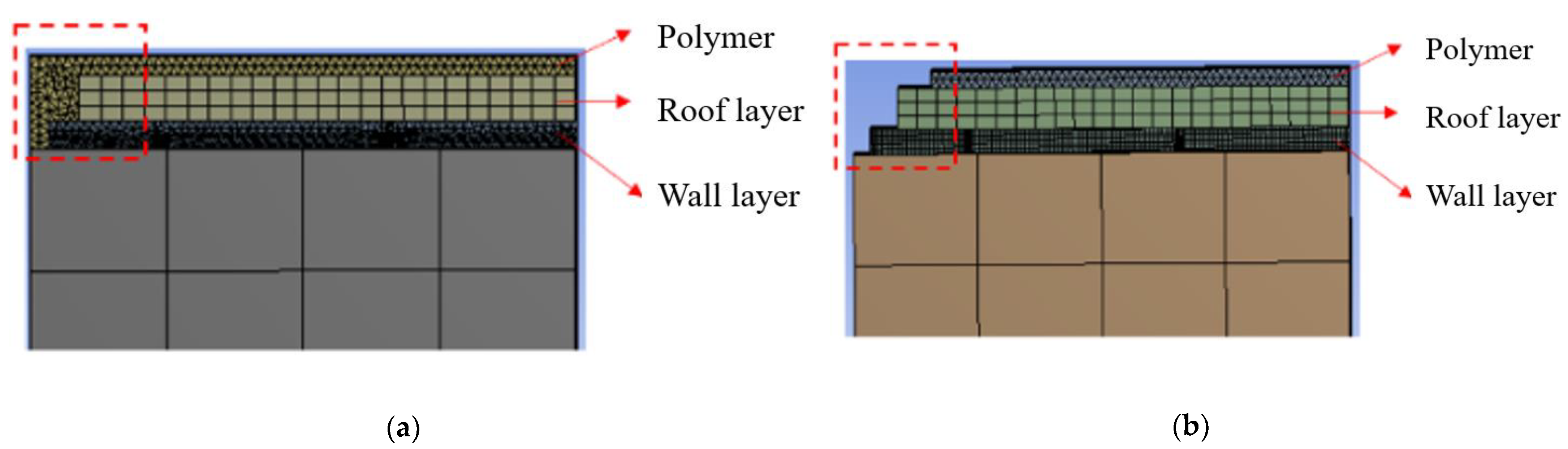
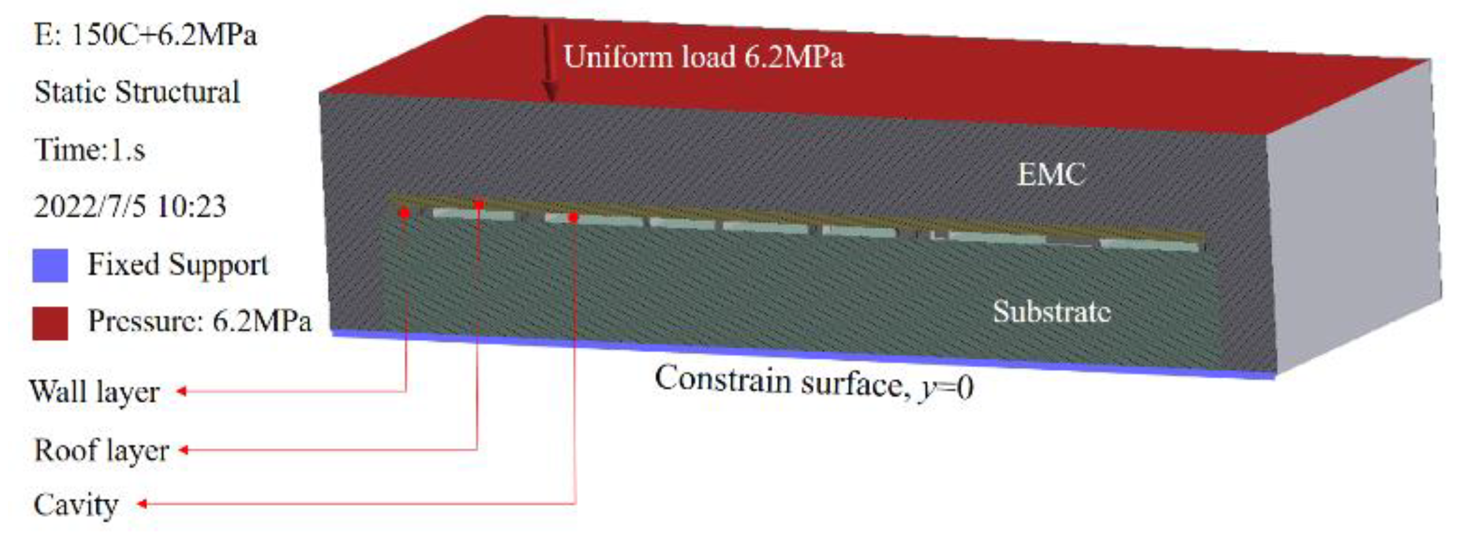
3.1. Single-Die FE Model to Solve the RDL Crack Failure Mode
3.2. Effect of Geometric Parameters on Stress Distribution
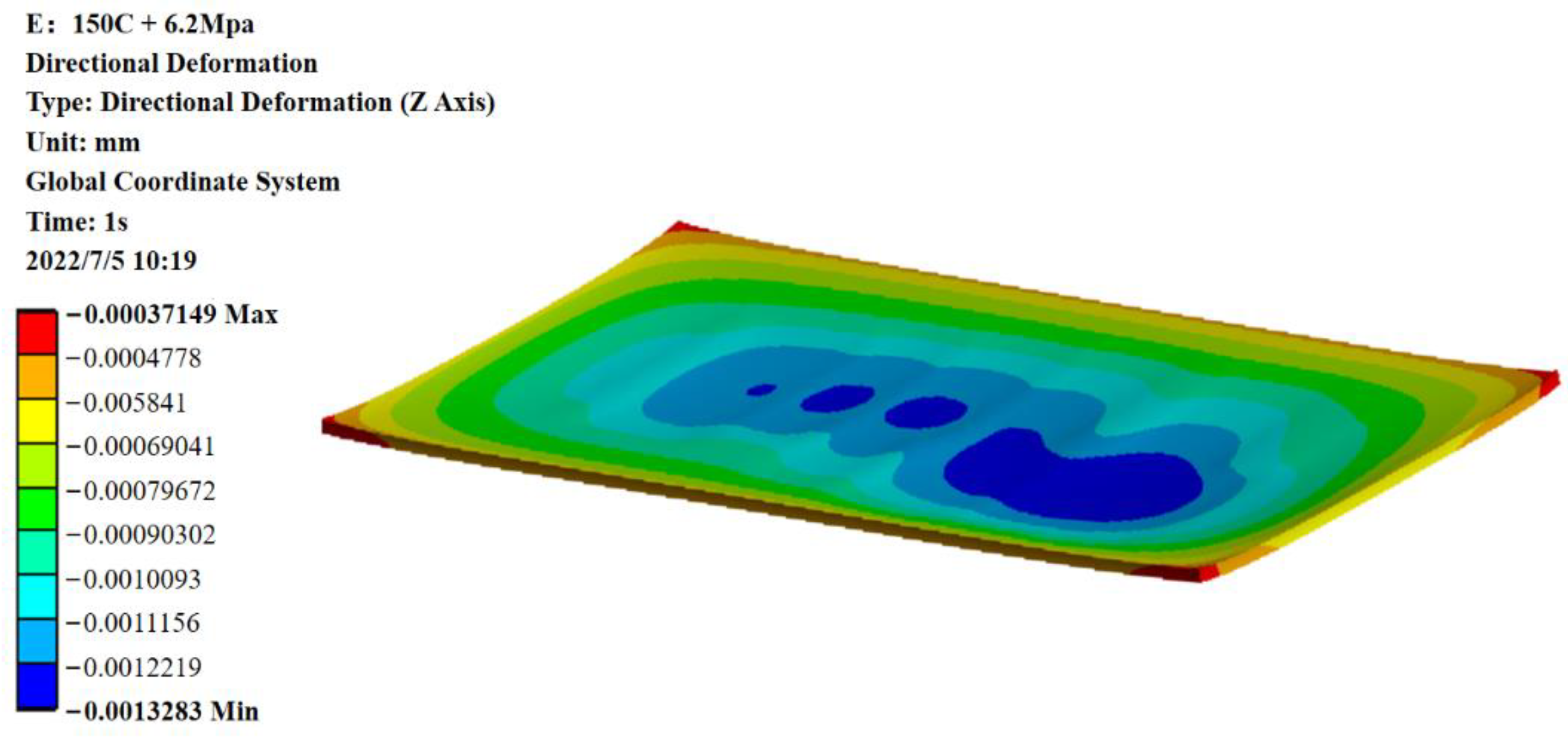
3.3. Deflection Prediction of Different Cavity Sizes
4. Reliability Evaluation
5. Conclusions
- (1)
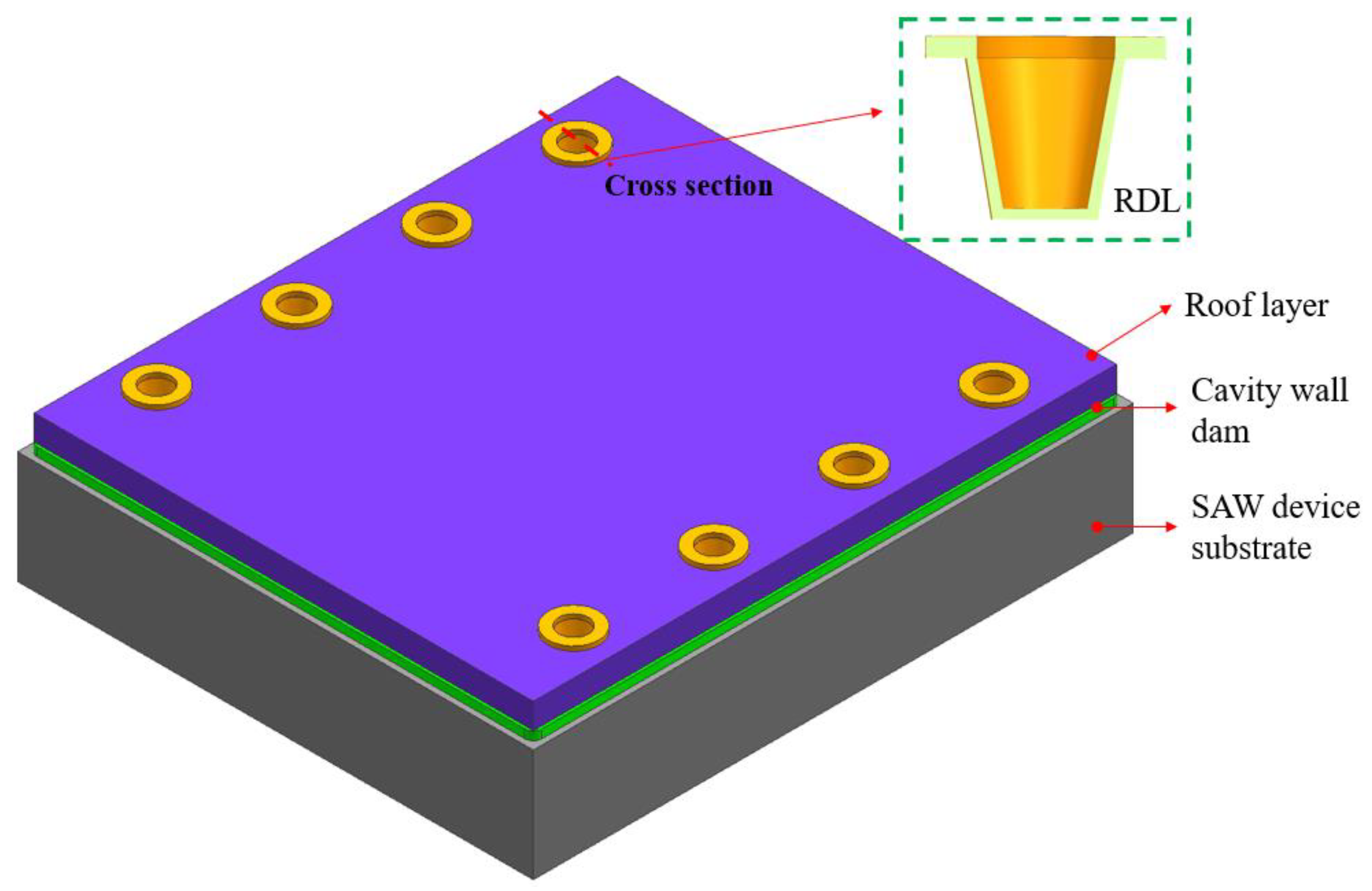
- A wafer-level lamination process was conducted on the SAW filter substrate with the CW dam layer together before the electrical interconnection process. Laser drilling was used to form the connection vias, which was characterized by a gradual increase in diameter from the bottom to the top of the TFVs, and the side walls were smooth without steps.
- (2)
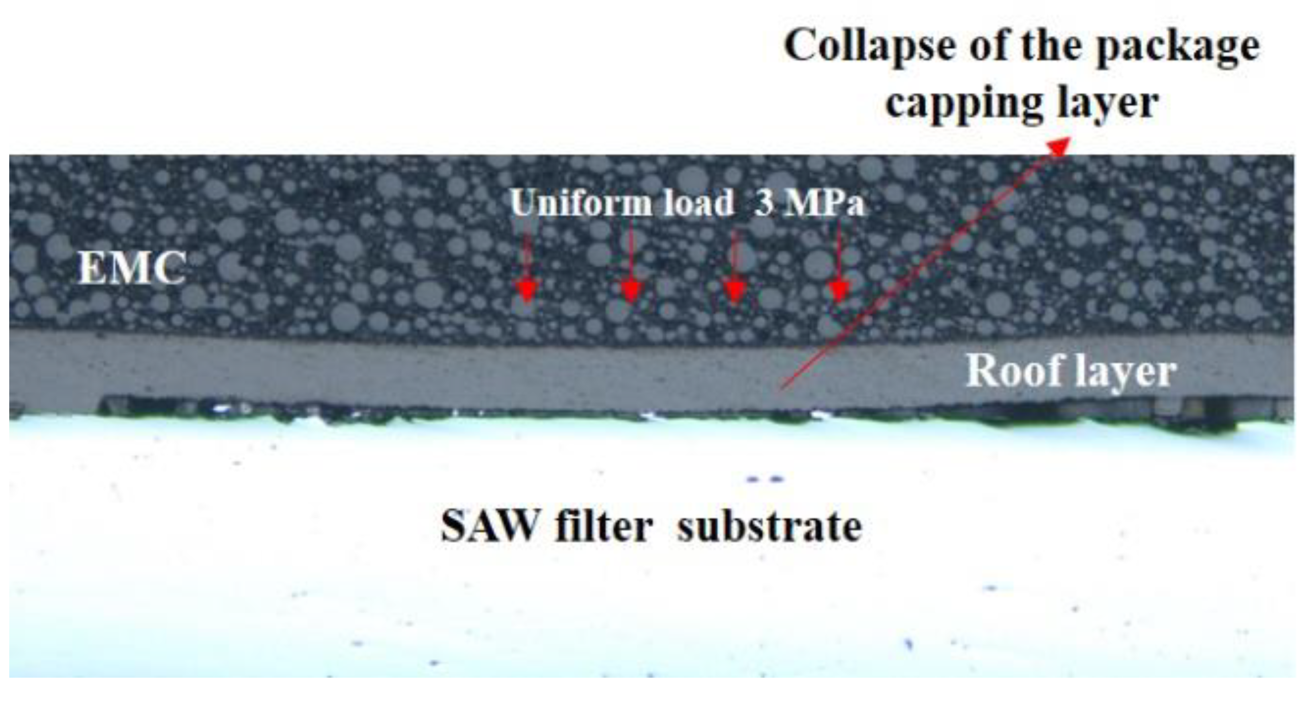
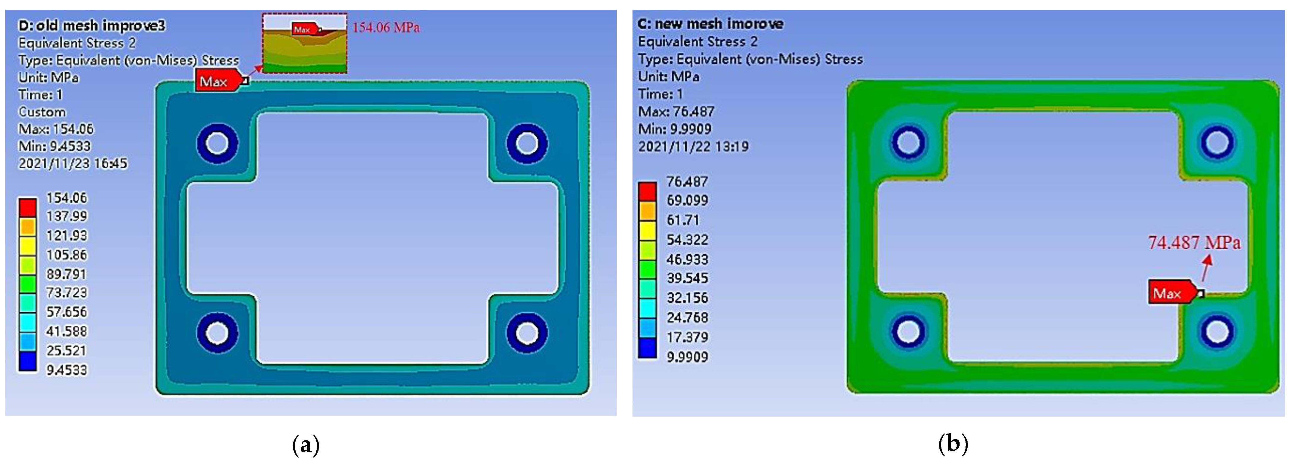
- Parameters, such as material properties and geometry, affect the maximum stress of the package significantly. Following practical verification, the cavity collapse amount was projected to be about 6.6 μm at a larger size of 980 μm × 320 μm, resolving the collapse problem caused by the encapsulating pressure of the SAW filter WLP. In terms of the effect of the geometric parameters on stress distribution, by comparing the top-side molded with the conventional SAW filter WLP, the maximum von Mises values were 74.487 MPa and 154.06 MPa, respectively, with a 51.65% reduction.
- (3)
- After Pre Con L3 and uHAST 96-h, no electrical breakdown was seen during the reliability tests. The results show that the proposed SAW filter package based on 3D WLP technology is reliable for large-scale industrial manufacture. We infer from this that our technique can significantly enhance the development and use of consumer market band applications.
6. Patents
Author Contributions
Funding
Institutional Review Board Statement
Informed Consent Statement
Data Availability Statement
Acknowledgments
Conflicts of Interest
References
- Watanabe, A.O.; Ali, M.; Sayeed, S.Y.B.; Tummala, R.R.; Pulugurtha, M.R. A Review of 5G Front-End Systems Package Integration. IEEE Trans. Compon. Packag. Manuf. Technol. 2021, 11, 118–133. [Google Scholar] [CrossRef]
- Gong, S.; Lu, R.; Yang, Y.; Gao, L.; Hassanien, A.E. Microwave Acoustic Devices: Recent Advances and Outlook. IEEE J. Microw. 2021, 1, 601–609. [Google Scholar] [CrossRef]
- Hagelauer, A.; Fattinger, G.; Ruppel, C.C.W.; Ueda, M.; Hashimoto, K.-Y.; Tag, A. Microwave Acoustic Wave Devices: Recent Advances on Architectures, Modeling, Materials, and Packaging. IEEE Trans. Microw. Theory Tech. 2018, 66, 4548–4562. [Google Scholar] [CrossRef]
- Chen, Z.; Yu, D.; Zhang, M.; Jiang, F. Development and Reliability Study of 3-D Wafer Level Packaging for SAW Filter Using Thin Film Capping. IEEE Trans. Compon. Packag. Manuf. Technol. 2021, 11, 1047–1054. [Google Scholar] [CrossRef]
- Chen, Z.; Yu, D.; Jiang, F. Development of 3-D Wafer Level Packaging for SAW Filters Using Thin Glass Capping Technology. IEEE Trans. Compon. Packag. Manuf. Technol. 2022, 12, 375–381. [Google Scholar] [CrossRef]
- Chen, Z.; Yu, D.; Jiang, F. A Wafer-Level Packaging Structure and Method for Filter. CN Patent 202210528805.8, 16 May 2022. [Google Scholar]
- Lim, J.-H.; Hwang, J.-S.; Kwon, J.; Ham, S.-J.; Kim, T.H.; Jeung, W.K.; Yang, S.J.; Choi, S.M.; Park, J.H.; Kim, W. 6B-6 An Ultra Small SAW RF Filter using Wafer Level Packaging Technology. In Proceedings of the 2006 IEEE Ultrasonics Symposium, Vancouver, BC, Canada, 3–6 October 2006; pp. 196–199. [Google Scholar] [CrossRef]
- Zoschke, K.; Wegner, M.; Lopper, C.; Klein, M.; Gruenwald, R.; Schoenbein, C.; Lang, K.-D. LiTaO3 Capping Technology for Wafer Level Chip Size Packaging of SAW Filters. In Proceedings of the 2016 IEEE 66th Electronic Components and Technology Conference (ECTC), Las Vegas, NV, USA, 31 May–3 June 2016; pp. 889–896. [Google Scholar] [CrossRef]
- Kim, T.H.; Jeung, W.K.; Yang, S.J.; Choi, S.M.; Park, S.W.; Kim, H.H.; Ha, J.; Park, M.J.; Kao, S.; Hong, J.; et al. Miniaturization and Optimization of RF SAW Filter Using Wafer Level Packaging Technology. In Proceedings of the 57th Electronic Components and Technology Conference, Las Vegas, NV, USA, 29 May–1 June 2007; pp. 574–579. [Google Scholar] [CrossRef]
- Pitschi, F.M.; Bauer, C.; Koch, R.D.; Wagner, K.C. Approaches to wafer level packaging for SAW components. In Proceedings of the 2013 IEEE MTT-S International Microwave Symposium Digest (MTT), Seattle, WA, USA, 2–7 June 2013; pp. 1–3. [Google Scholar] [CrossRef]
- Ham, S.-J.; Jeong, B.-G.; Lim, J.-H.; Jung, K.-D.; Baek, K.-D.; Kim, W.-B.; Moon, C.-Y. Characterization and Reliability Verification of Wafer-Level Hermetic Package with Nano-Liter Cavity for RF-MEMS Applications. In Proceedings of the 57th Electronic Components and Technology Conference, Sparks, NV, USA, 29 May 2007–1 June 2007; pp. 1127–1134. [Google Scholar] [CrossRef]
- Park, S.W.; Hong, J.P.; Kim, T.H.; Yang, S.J.; Ha, J.; Park, S.W.; Kweon, Y.D.; Yi, S. Fabrication and optimization of wafer level SAW filter package using laser via drilling. In Proceedings of the 2nd Electronics System-Integration Technology Conference, Greenwich, UK, 1–4 September 2008; pp. 1273–1278. [Google Scholar] [CrossRef]
- Kawachi, O.; Sakinada, K.; Kaneda, Y.; Ono, S. P3N-2 Packaging of SAW Devices with Small, Low Profile and Hermetic Performance. In Proceedings of the IEEE Ultrasonics Symposium, Vancouver, BC, Canada, 3–6 October 2006; pp. 2289–2292. [Google Scholar] [CrossRef]
- Feiertag, G.; Krüger, H.; Bauer, C. Surface acoustic wave component packaging. In Proceedings of the European Microelectronics and Packaging Conference, Oulu, Finland, 17–20 June 2007; pp. 1–5. [Google Scholar]
- Mandal, D.; Banerjee, S. Surface Acoustic Wave (SAW) Sensors: Physics, Materials, and Applications. Sensors 2022, 22, 820. [Google Scholar] [CrossRef]
- Savornin, B.; Baillin, X.; Blanquet, E.; Nuta, I.; Patrice, D.S.; Nicolas, P.; Charvet, P.L.; Pornin, J.L. Outgassing characterization of MEMS thin film packaging materials. In Proceedings of the IEEE 63rd Electronic Components and Technology Conference, Las Vegas, NV, USA, 28–31 May 2013; pp. 1514–1518. [Google Scholar] [CrossRef]
- Zhou, T.; Ma, S.; Yu, D.; Li, M.; Hang, T. Development of Reliable, High Performance WLCSP for BSI CMOS Image Sensor for Automotive Application. Sensors 2020, 20, 4077. [Google Scholar] [CrossRef]
- Fukano, T.; Okubo, Y.; Nishii, J.; Obara, I. 2E-2 0806 SAW Filters Using Wafer Level Packaging Technology. In Proceedings of the IEEE Ultrasonics Symposium, New York, NY, USA, 28–31 October 2007; pp. 68–71. [Google Scholar] [CrossRef]
- Qin, F.; Zhao, S.; Dai, Y.; Yang, M.; Xiang, M.; Yu, D. Study of Warpage Evolution and Control for Six-Side Molded WLCSP in Different Packaging Processes. IEEE Trans. Compon. Packag. Manuf. Technol. 2020, 10, 730–738. [Google Scholar] [CrossRef]
- Hsiao, H.-Y.; Ho, D.S.W.; Chong, S.C.; Chai, T.C.; Schutzberger, D.; Oz, Y.; Amrani, G. Through Mold Via Development Using Laser Drilling Process for 3D Fan-out Wafer Level Package. In Proceedings of the IEEE 23rd Electronics Packaging Technology Conference (EPTC), Virtual, 1–3 December 2021; pp. 253–257. [Google Scholar] [CrossRef]
- Hsiao, H.-Y.; Ho, D.S.W.; Lim, K.C.S.; Chong, S.C.; Chai, T.C.; Schutzberger, D.; Oz, Y.; Amrani, G.; Zhao, J.; Toh, J. Laser drilling and Plasma Cleaning Process for Blind Via Through Mold Interconnect. In Proceedings of the IEEE 22nd Electronics Packaging Technology Conference (EPTC), Singapore, 2–4 December 2020; pp. 14–18. [Google Scholar] [CrossRef]
- Zhao, J.; Li, W.; Zhong, Y.; Yu, D.; Qin, F. Stress Issues in 3D Interconnect Technology Using Through Glass Vias. J. Mech. Eng. 2022, 58, 246–258. [Google Scholar] [CrossRef]
- Zhao, J.; Qin, F.; Yu, D.; Chen, Z.; Zhao, S. Warpage Characteristic of Glass Interposer with Different CTE’s and Thickness. In Proceedings of the 22nd International Conference on Electronic Packaging Technology (ICEPT), Xiamen, China, 11–14 August 2021; pp. 1–4. [Google Scholar] [CrossRef]
- Li, Q.; Goosen, H.; Van Keulen, F.; Van Beek, J.; Zhang, G. Assessment of testing methodologies for thin-film vacuum MEMS packages. Microsyst. Technol. 2009, 15, 161–168. [Google Scholar]


| Items | Young Modulus | Poisson Ratio | CTE |
|---|---|---|---|
| SAW device substrate | 230 Gpa | 0.22 | 16.1 ppm/°C 4.1 ppm/°C |
| Cavity wall layer | 4.4 Gpa | 0.34 | 65 ppm/°C |
| Roof layer | 9 Gpa | 0.34 | CTE1: 18 ppm/°C (25–150 °C) CTE2: 45 ppm/°C (150–240 °C) |
| Cu | 119 Gpa | 0.326 | 17.5 ppm/°C |
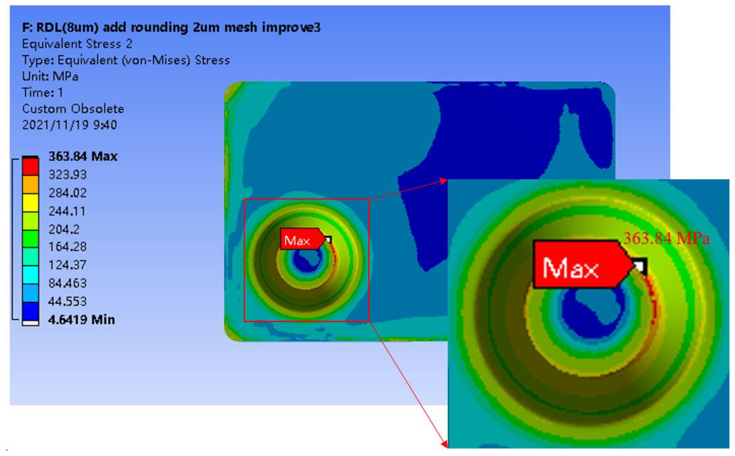
| Cu Thickness | Stress Point (MPa) | Ratio |
|---|---|---|
| 2 µm | 416.07 | 1.00 |
| 8 µm | 363.84 | 1.14 |
| filled via | 350.45 | 1.19 |
| Items | Conditions | Failure Rate (%) | Result | |
|---|---|---|---|---|
| Pre-Con L3 | Bake | 125 °C/24 H | 0.00 | Pass |
| Soak | 30 °C/60%/192 H | 0.00 | Pass | |
| Reflow | 260 °C (+5/−0) 3× | 0.00 | Pass | |
| uHAST | 130 °C/85% RH, 96 H | 0.00 | Pass | |
Publisher’s Note: MDPI stays neutral with regard to jurisdictional claims in published maps and institutional affiliations. |
© 2022 by the authors. Licensee MDPI, Basel, Switzerland. This article is an open access article distributed under the terms and conditions of the Creative Commons Attribution (CC BY) license (https://creativecommons.org/licenses/by/4.0/).
Share and Cite
Chen, Z.; Yu, D. Development of a Reliable High-Performance WLP for a SAW Device. Sensors 2022, 22, 5760. https://doi.org/10.3390/s22155760
Chen Z, Yu D. Development of a Reliable High-Performance WLP for a SAW Device. Sensors. 2022; 22(15):5760. https://doi.org/10.3390/s22155760
Chicago/Turabian StyleChen, Zuohuan, and Daquan Yu. 2022. "Development of a Reliable High-Performance WLP for a SAW Device" Sensors 22, no. 15: 5760. https://doi.org/10.3390/s22155760
APA StyleChen, Z., & Yu, D. (2022). Development of a Reliable High-Performance WLP for a SAW Device. Sensors, 22(15), 5760. https://doi.org/10.3390/s22155760