Communication

A Design of 10-Bit Asynchronous SAR ADC with an On-Chip Bandgap Reference Voltage Generator

1
Department of Electrical and Computer Engineering, Sungkyunkwan University, Suwon 16419, Korea
2
SKAIChips Co., Ltd., Suwon 16419, Korea
*
Author to whom correspondence should be addressed.
Sensors 2022, 22(14), 5393; https://doi.org/10.3390/s22145393
Submission received: 22 June 2022 / Revised: 16 July 2022 / Accepted: 18 July 2022 / Published: 19 July 2022

Abstract

:
A proposed prototype of a 10-bit 1 MS/s single-ended asynchronous Successive Approximation Register (SAR) Analog-to-Digital Converter (ADC) with an on-chip bandgap reference voltage generator is fabricated with 130 nm technology. To optimize the power consumption, static, and dynamic performance, several techniques have been proposed. A dual-path bootstrap switch was proposed to increase the linearity sampling. The Voltage Common Mode (VCM)-based Capacitive Digital-to-Analog Converter (CDAC) switching technique was implemented for the CDAC part to alleviate the switching energy problem of the capacitive DAC. The proposed architecture of the two-stage dynamic latch comparator provides high speed and low power consumption. Moreover, to achieve faster bit conversion with an efficient time sequence, asynchronous SAR logic with an internally generated clock is implemented, which avoids the requirement of a high-frequency external clock, as all conversions are carried out in a single clock cycle. The proposed error amplifier-based bandgap reference voltage generator provides a stable reference voltage to the ADC for practical implementation. The measurement results of the proposed SAR ADC, including an on-chip bandgap reference voltage generator, show an Effective Number of Bits (ENOB) of 9.49 bits and Signal-to-Noise and Distortion Ratio (SNDR) of 58.88 dB with 1.2 V of power supply while operating with a sampling rate of 1 MS/s.

1. Introduction

For low-power applications, a Successive Approximation Register (SAR) analog-to-digital converter (ADC) is a good choice to obtain successive digital code from an analog input by using the binary search algorithm. Due to its simplicity and power efficiency, SAR ADC is more popular and favorable for comparison with other types of ADCs [1,2,3]. Traditionally, pipeline ADCs have been frequently used for high-speed and medium-resolution data converters. However, the down-scaling of CMOS technologies and reduction in the power supply voltages arouses some significant obstacles for the power-efficient design of pipeline ADCs, because pipeline ADCs have need for high-gain operational amplifiers, which increases the power consumption of pipeline ADCs. In addition to this, it also degrades the swing of amplifiers, which results in the reduction of the Signal-to-Noise Ratio (SNR) for the provided sampling capacitance value. Additionally, the operational amplifier needs to have high DC gain, which lowers the power efficiency because of the low output resistance from short-channel-length devices. On the other hand, SAR ADCs abolish the requirement for an operational amplifier and can attain magnificent power efficiency [4,5]. According to the present trend, SAR ADC provides a sampling speed of several tens of MS/s for medium resolution, which permits the design of low-power and high-performance ADCs. SAR ADCs also have the characteristic of power dissipation being directly related to the sampling rate. These features of SAR ADCs make them the ideal candidate for many applications, such as data signal acquisition, battery management systems, pen digitizers, etc. The simple concept of the SAR ADC is that the analog input will be held by the sample and then be compared with the reference voltage of the ADC, which is an output of the DAC. A stable reference voltage is required for high-resolution ADCs. For SAR ADCs, static bias current is not required in the design of the dynamic comparator [6,7]; hence, the overall power consumption of SAR ADC scales with the sampling rate.
In the SAR ADC, the analog input signal is compared with the reference voltage by a comparator. This reference voltage should be stable and independent of the environmental condition for the stable analog-to-digital conversion [8]. The reference voltage can also be generated by the supply voltage, but it suffers around ±10% of variation [9]; hence, SAR ADC requires a high-precision reference voltage generated by an on-chip bandgap reference voltage generator circuit [10]. The reference voltage cannot vary with the operating conditions, but it can change within the small range of process, voltage, and temperature (PVT) variations [8,11,12]. Furthermore, parasitic inductance affects the reference voltage line and degrades the overall ADC performance when the reference voltage is generated off-chip. In order to achieve the targeted SAR ADC performance, it requires an on-chip reference voltage generator circuit.
In this work, we present a power-efficient single-ended asynchronous SAR ADC implemented in 130 nm CMOS technology. The proposed dual-path bootstrap switch reduces the sampling nonlinearity. The VCM-based switching sequence is proposed, which reduces the capacitive DAC total capacitance by half due to the additional reference of VCM. For high speed and power efficiency, we implemented a two-stage dynamic latch comparator. To overcome the speed limitation, which is caused by the capacitive DAC settling, an on-chip bandgap reference voltage generator has been implemented. The design details and topology of a dual-path bootstrap switch, capacitive DAC, a two-stage dynamic comparator, asynchronous SAR logic, and an error amplifier-based bandgap reference voltage generator that satisfies the performance requirements are further discussed in detail.
The proposed single-ended asynchronous SAR ADC architecture is described in Section 2. The sub-blocks of the proposed asynchronous ADC, such as dual-path bootstrap switching, VCM-based capacitive DAC switching, two-stage dynamic latch comparator, asynchronous SAR logic, and error-amplifier-based bandgap reference voltage generator are described in Section 3, and the measurement results are presented in Section 4. Finally, we conclude the paper in Section 5.

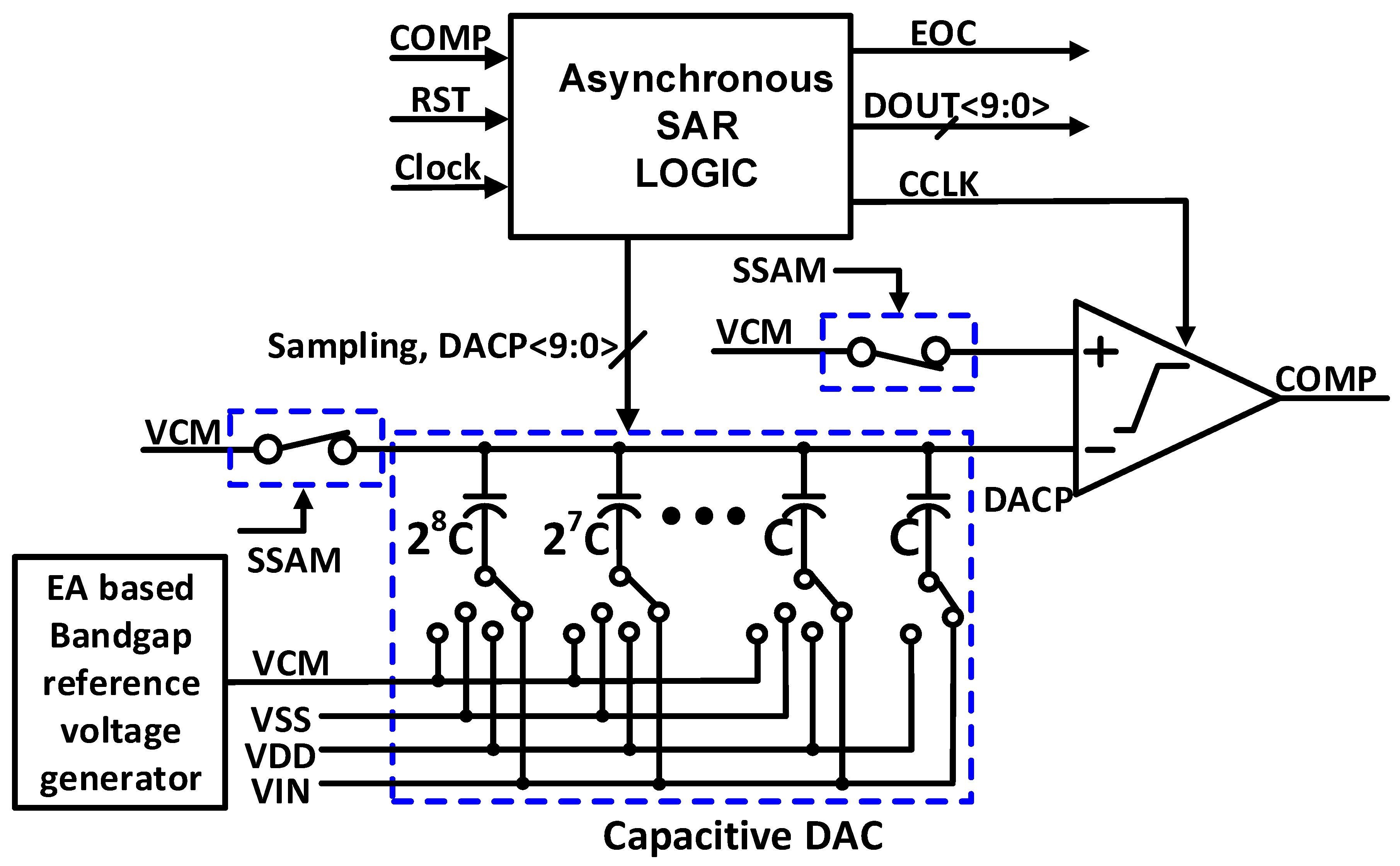
2. Proposed ADC Architecture

The proposed single-ended asynchronous SAR ADC topology is designed and fabricated for a 10-bit resolution with a sampling speed of 1 MS/s, and the architecture is presented in Figure 1. The proposed SAR ADC contains a binary weighted capacitive DAC, a bootstrap switch, dynamic comparator, asynchronous SAR logic with an internal comparator clock generator, and a bandgap reference generator. A dual-path bootstrap switch is presented that overcomes the sampling nonlinearity. The VCM-based switching sequence is proposed, which reduces the capacitive DAC’s total capacitance by half due to the additional reference of VCM. Owing not only to the reduced capacitance, but also to the reduced switching step size as well as the removed switching-back operation, the VCM-based CDAC switching achieves excellent energy efficiency. The capacitive DAC is controlled by the digital output code, which is stored by asynchronous SAR logic and the decision made by the comparator. In the proposed single-ended asynchronous SAR ADC, a reference voltage of 0.6 V is generated by the error amplifier (EA)-based bandgap reference voltage generator. The 10-bit capacitive DAC provides the reference voltage DACP to the one input of the comparator, and the other input comparator has common-mode voltage (VCM). The sampling and hold operation is conducted by the sampling switch and capacitive DAC capacitors. The sampling signal, DACP<9:0>, CCLK, and SSAM are the control signals generated from the asynchronous SAR logic. The CCLK signal is provided to the comparator for the fast comparison of the comparator. For high speed and power efficiency, we implemented a two-stage dynamic latch comparator. In addition to this, for practical use, we implemented an on-chip bandgap reference voltage generator that provides better stability and reduced offset voltage distribution.

3. Circuit Implementation

3.1. Bootstrap Switching
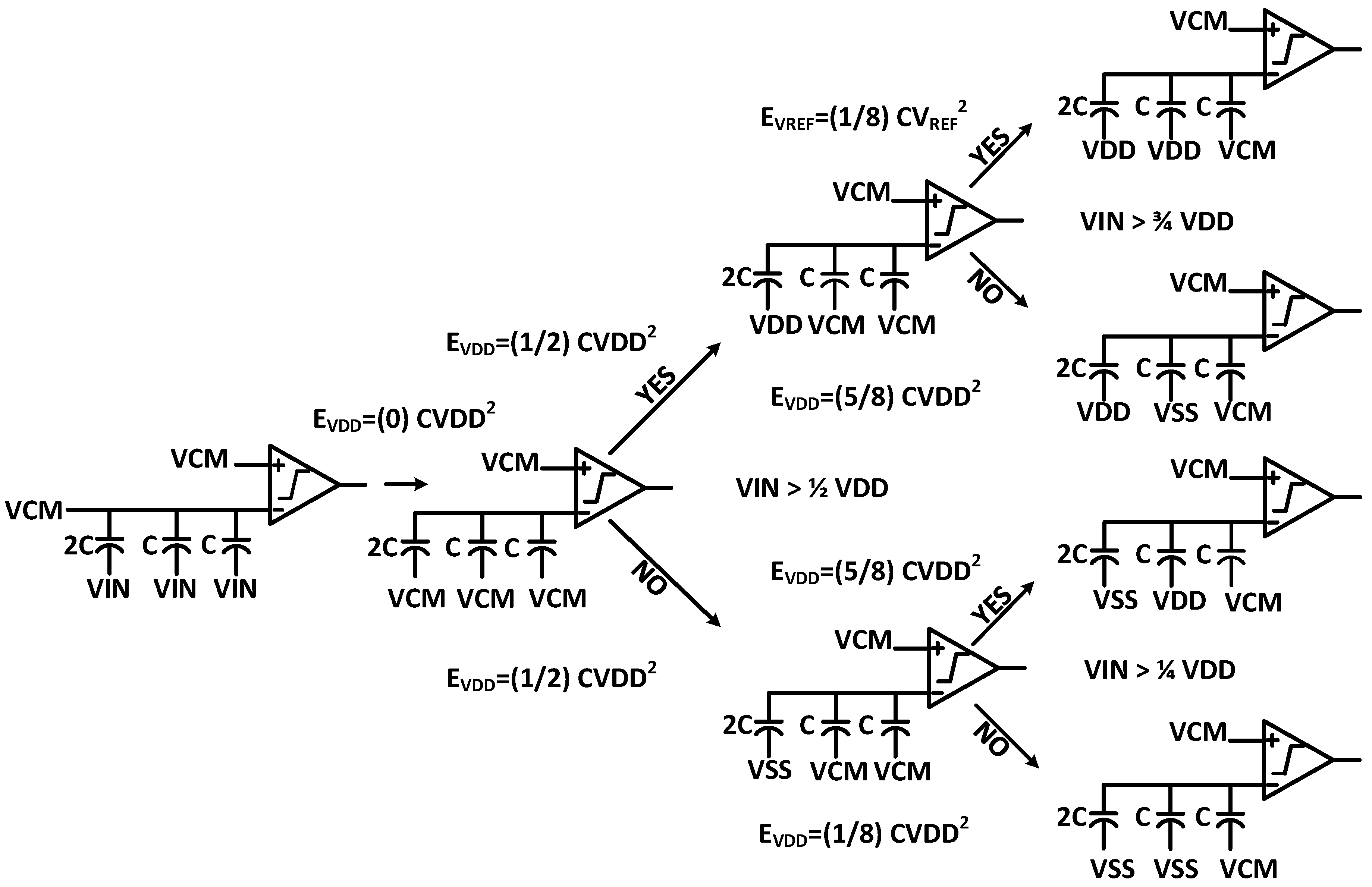
Nowadays, for linear sampling, a bootstrap switch is frequently used, and its non-idealities have become pronounced; thus, its linearity is seriously degrading. Several techniques have been used to improve the performance of the bootstrap switch, such as modifying the circuit network or incorporating fast-turn-on circuits [13]. In Figure 2, we propose a technique to improve the linearity of the bootstrap switch. Ideally, to achieve the constant switch on-conductance, the Vgs of the sampling transistor M10 is independent of and constant with the input. The proposed technique integrates the dual-path bootstrap switch to improve the sampling nonlinearity, and operates at the sampling rate of 1 MS/s, with a 50% duty cycle and peak-to-peak voltage of 600 mV, as shown in Figure 2. This technique creates two paths for the signal; one is the main path, which contains M2 and C2, and the other is an auxiliary path, which contains M1 and C1. In the auxiliary path, the PMOS transistor’s M1, M2, and M4’s bulk terminals are connected to the VX node, which prevents forward biasing. By the proposed dual-path bootstrap switching technique, the nonlinear capacitance drives through the auxiliary path, while the gate of the sampling switch propagates the input signal, and hence the nonlinear capacitance is not directly being loaded into the main path. In this way, we can maximize the drive strength and signal linearity by independently optimizing the auxiliary path and the main path. The formula for voltage transfer to Vg from VIN and its phase are expressed as follows:
V g VIN = ( sR 4 C g + C g C 2 + 1 ) 1
ϕ = ω IN R 4 C g ( 1 + C g C 2 ) 1
where R4 = 1/G4, G4 is the on conductance of transistor M4, and Cg is the gate capacitance of transistor M10. By the proposed bootstrap switch, G4 is more linear because, instead of the supply voltage VDD, the bulk of M4 is connected to the nonlinear voltage VX. Therefore, the square root of the error of nonlinear voltage VX is directly proportional to G4. Hence, to improve the nonlinearity, the nonlinear voltage VX goes through the bulk of M4, and nonlinear parasitic capacitance from the main path is removed by C2.

3.2. Capacitive DAC

Various circuit techniques could further enhance the low power advantage of SAR ADCs. A large amount of research has been conducted to save the CDAC’s switching power consumption. Unlike the traditional SAR ADC architecture with two voltage references, the VCM-based switching scheme proposed could reduce the total capacitance of the CDAC by half due to the additional reference of VCM. It does not only reduce the overall CDAC capacitance, but also reduces the switching step size. With the removed switching-back operation, the VCM-based CDAC switching could achieve excellent energy efficiency and become popular for low-power designs. One drawback of the VCM-based switching scheme might be the difficulty in designing low-resistance switches for VCM. The monotonic switching technique can eliminate the need for VCM by the asymmetric CDAC switching, but this scheme has a varying common-level problem [14,15]. The energy-saving switching technique could implement VCM-based-like switching behavior without utilizing VCM by splitting each capacitor in half. The improved process controllability of advanced CMOS technologies also contributed to reducing the CDAC switching power consumption by decreasing the minimum unit capacitor values without the need for a dedicated process for capacitor implementation.
The proposed CDAC switching with the binary weighted array used in the single-ended SAR ADC is depicted in Figure 3. In the sampling phase, the bottom plates of all capacitors are connected to the VCM and the top plates are connected to the VIN. Thus, the input voltage is sampled on the binary weighted capacitor array, and we obtain the first signed bit without consuming any switching energy. Depending on the first signed bit, the next conversion cycle is either charged to VDD or discharged to VSS from VCM. Hence, the MSB capacitor is not required in the proposed switching scheme. The sensitivity due to the capacitor mismatch, dynamic, and static performance of the proposed capacitive DAC switching scheme is checked based upon the behavioral simulation in MATLAB. The fast Fourier transform (FFT) spectrum of the behavioral model-level simulation is evaluated in MATLAB® for the proposed switching architecture with 1% unit capacitor mismatch, as shown in Figure 4. The static performance metrics, differential non-linearity (DNL), and the integral non-linearity (INL) of the proposed switching with 1% unit capacitor mismatch are shown in Figure 5a,b respectively.
Figure 6 shows the output of the capacitive DAC (DACP) settling of input signals according to the clock signal. An end-of-conversion (EOC) signal will be generated after the completion of the conversion cycle based on the asynchronous SAR logic.

3.3. Two-Stage Dynamic Comparator

In the proposed two-stage dynamic latched comparator, two inverters are added to make the Vi node’s voltage strong by providing a higher regeneration speed, as shown in Figure 7. The proposed architecture of the two-stage dynamic latch comparator provides high speed and power efficiency, and lowers the input-referred offset compared with conventional comparator architecture [16,17,18]. When the clock signal CCLK is turned off, the PMOS transistors M11 and M12 are on, then the Vi nodes are charged to VDD, and VBi nodes are discharged to VSS during the reset phase. Consequently, there is no static power dissipation and static path due to charge sharing, and no DC flows in the static state of the proposed comparator. The NMOS transistors M9 and M10 drain, and output nodes charge to VDD, while the PMOS transistors of the regeneration stage turn on, and the VBi nodes discharge to VSS.
In the evaluation phase, when the clock signal CCLK increases, the Vi nodes discharge to VSS depending on the input voltage through the input transistors M13 and M14, and the tail transistor M15. The VBi nodes are charged from VSS to VDD, while the Vi nodes are discharged to VSS in the evaluation phase. Other transistors will be turned on when the NMOS transistors M9 and M10 are turned on in the second stage and either of the VBi nodes reaches the threshold voltage Vth. Consequently, the latch is activated and regenerates the digital voltage at the output.

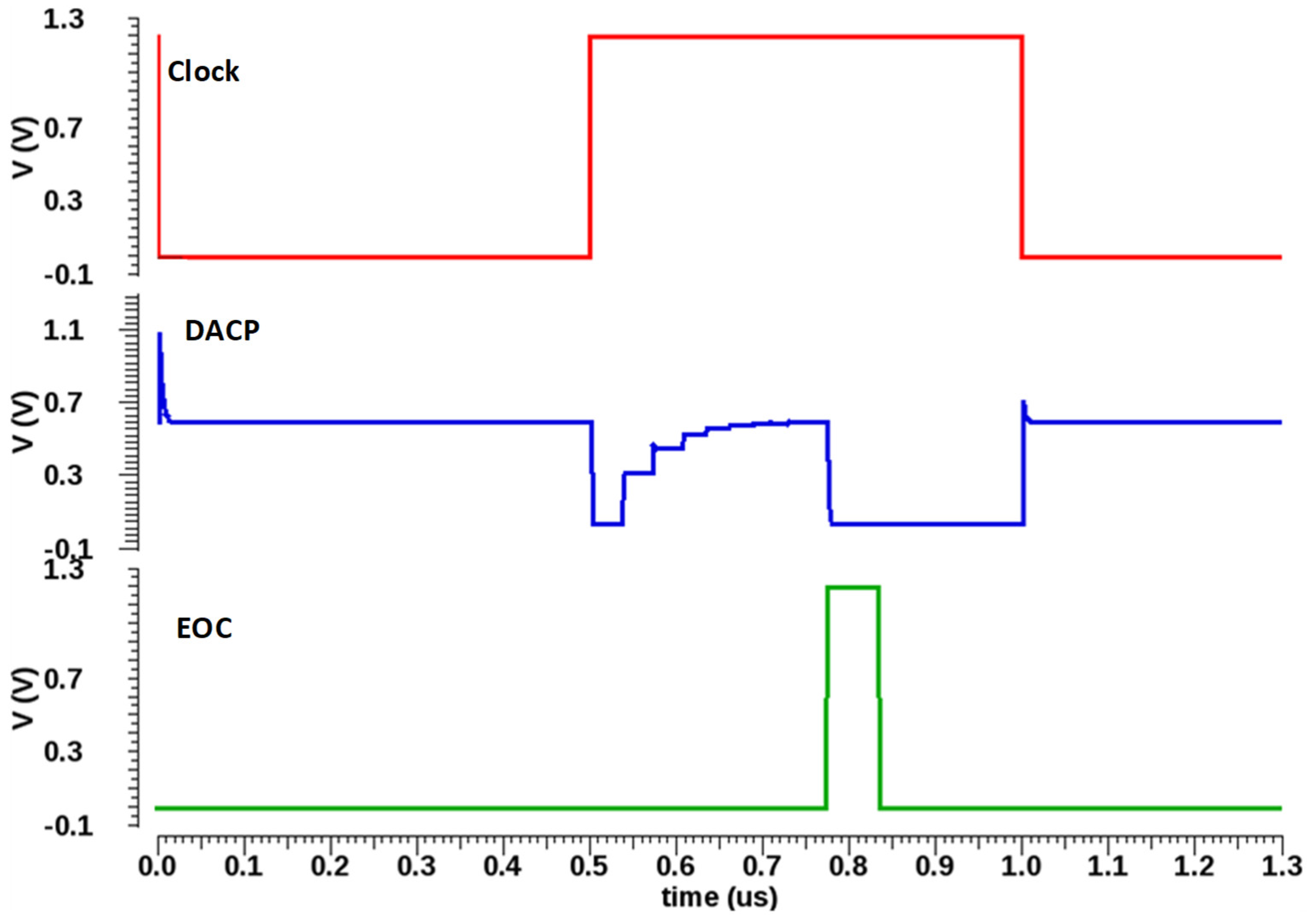
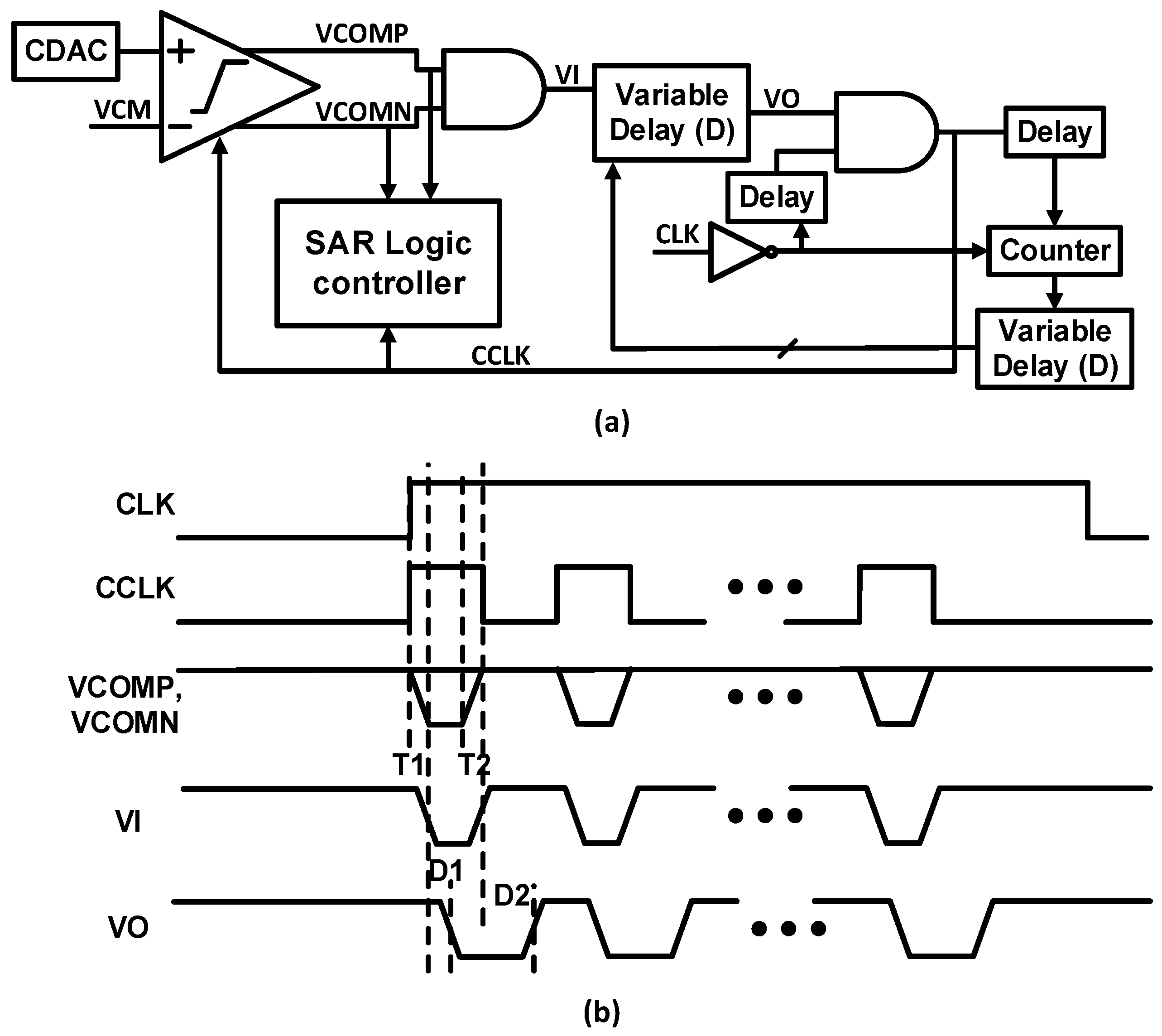
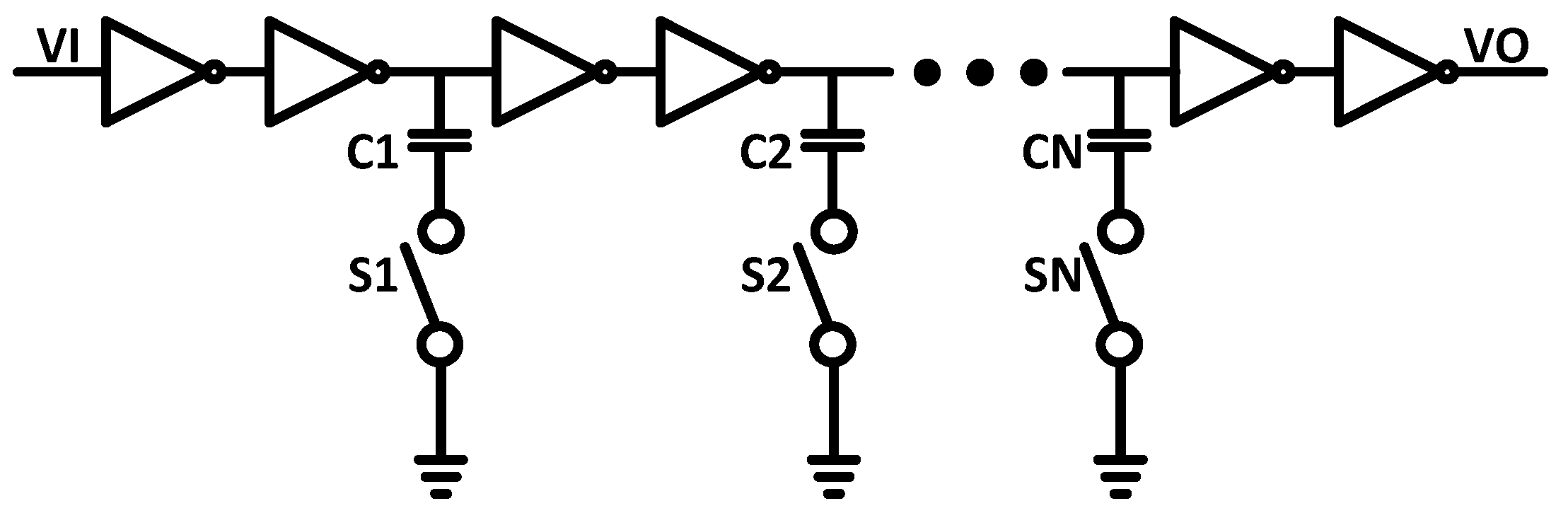
3.4. Asynchronous SAR Logic and Comparator Clock Generator

To achieve faster bit conversion with an efficient time sequence, asynchronous SAR ADC is more popular [19,20]. Asynchronous SAR logic with an internally generated clock avoids the requirement for the high-frequency external clock, as all conversions are carried out in a single clock cycle. Asynchronous SAR control logic is implemented for a shorter critical path.
A clock generator for SAR control logic is proposed, as shown in Figure 8a. The asynchronous clock generator consists of a delay cell, variable delay, an edge counter, delay adjust block, and logic gates. VCOMP or VCOMN are low, which allows VI to decrease after the decision of the comparator. Then, after the variable delay, VO is also low, which makes the CCLK decrease, and the SAR logic controller is triggered. The comparator starts the comparison when the reset of the comparator is completed, and VI, VO, and CCLK increase. To maximize the sampling period of conversion and to adjust the time delay, the delay adjust block and counter are used in feedback.
CCLK provides the reset time of the comparator and more time for DAC settling, as shown in Figure 8b. The proposed clock generator eliminates the memory effect in the comparator and speeds up the bit conversion. Hence, it also helps to improve the ADC robustness. The timing diagram of the proposed clock generator is shown in Figure 8b. The comparator’s decision time and reset time are represented as T1 and T2, respectively. D1 and D2 are the delay time, and unequal D1 and D2 can be obtained by the variable delay cell, as depicted in Figure 9. The variable delay cell is composed of an inverter array, implemented to achieve the desired variable delay. The arrangement of the inverter array leads the delay D1 to be small for the falling edge from VI to VO and delay D2 to be large for the rising edge.

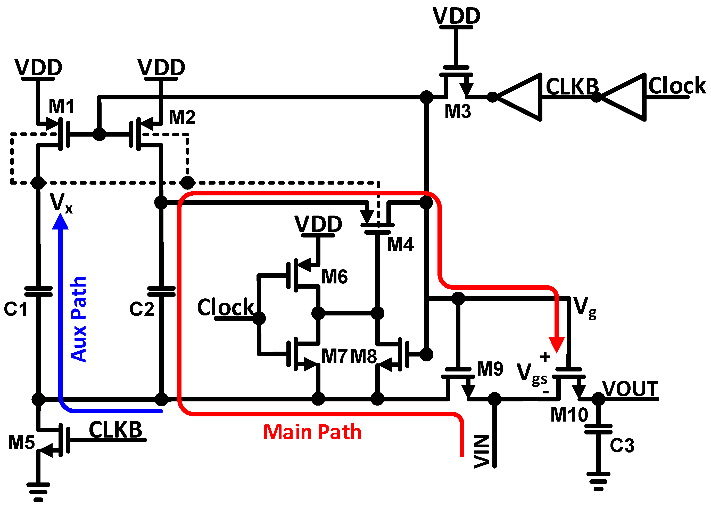
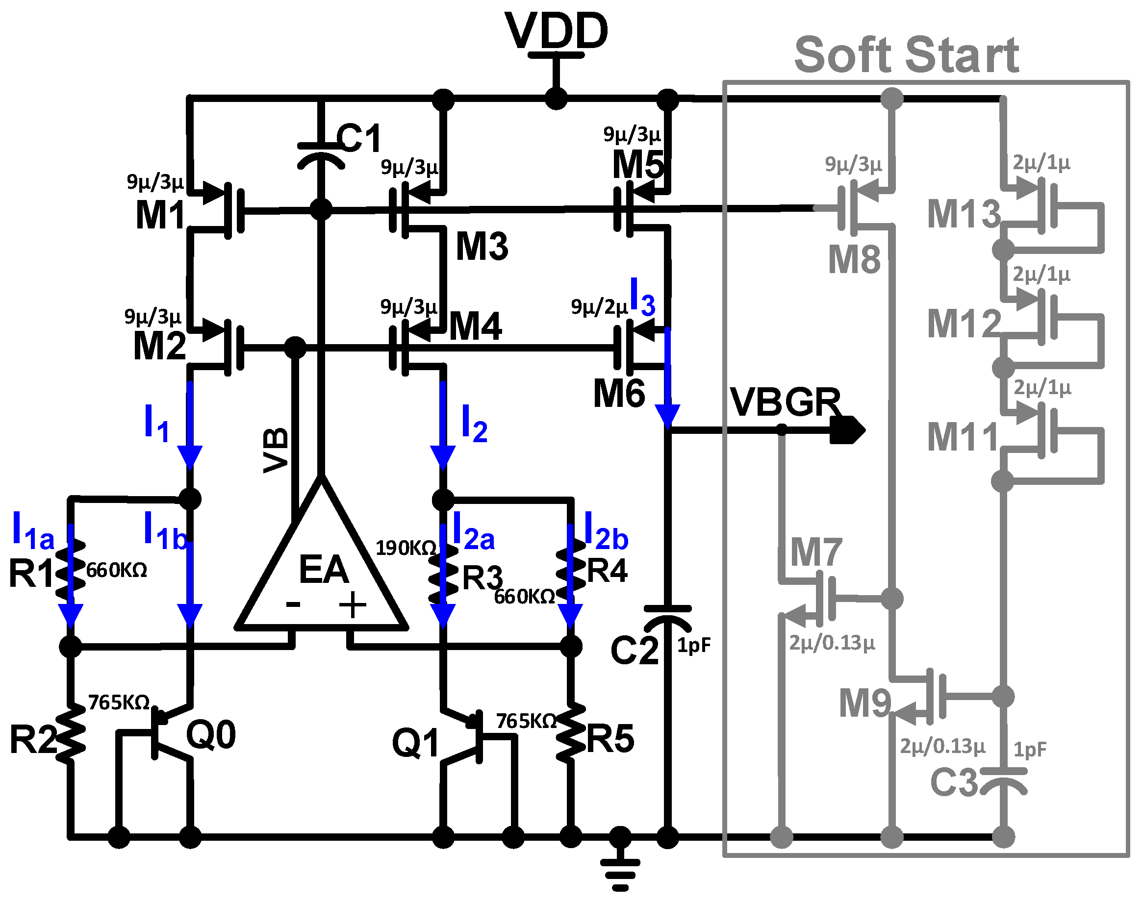
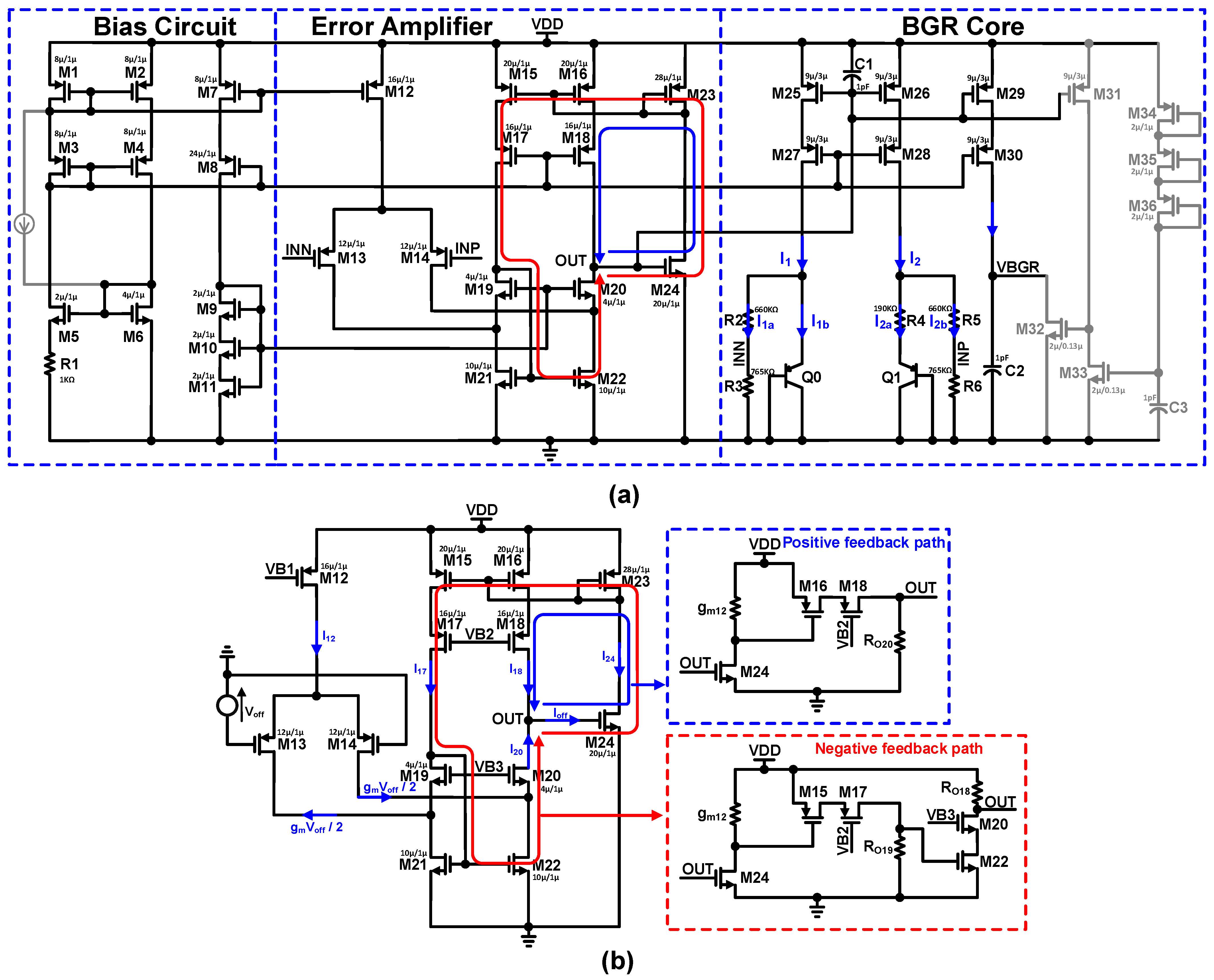
3.5. Error Amplifier-Based Bandgap Reference Voltage Generator

Reference voltage generators are required to stabilize the overall PVT variation, and also need to be implemented without modifying the fabrication process [21,22,23]. The bandgap reference voltage generator (BGR) is a popular reference voltage generator that successfully achieves the requirements [24,25]. Low power and low voltage operation are the characteristics of reference voltage generators. The error amplifier feedback keeps the same voltage level at both inputs of EA, and R3 generates the voltage difference between the two BJTs, as represented in Figure 10. A Soft-Start circuit is added to the output; when the power signal is high, a current starts to flow through the PMOSs, M11, M12, and M13 connected in diode fashion. To prevent the BGR peak voltage, it slowly charges the capacitor C3, and the BGR output voltage rises. The output of the error amplifier controls the gate of transistors M1 and M3 so that the input voltages of the error amplifier are equal. The positive feedback and negative feedback improve the loop stability of the proposed error amplifier. A detailed schematic of the error amplifier-based BGR circuit is shown in Figure 11a. VB1, VB2, and VB3 are the biasing voltages provided by the bias circuit to the cascaded error amplifier. We assume that the transistors M15–M18 and M23 are matched in terms of their aspect ratios, and the drain current of M18 is represented as:
I 18 = I 17 = I 15 = I 16 = I 24 = g m 24 2 ( OUT V THn ) = g m 16 2 ( V d s 23 V THp )
Initially, Voff caused the output offset current Ioff of the proposed error amplifier circuit shown in Figure 11b. Between the feedback stage and cascade stage output, OUT triggers the two opposite currents. The offset currents I18 and I20 are the positive feedback path and negative feedback path, respectively, and act contrary to each other. Therefore, the output offset current Ioff is expressed as follows:
I off = I 18 I 20 = I 18 ( I 22 I 14 )
I off = g m 16 V o v 16 2 + g m 14 V off 2 g m 22 V o v 22 2
where Vov is the overdrive voltage; Vov = OUT − VTH and I20 = gmVoff/2. By carefully setting the overdrive voltage Vov and transconductance gm, we can alleviate the output offset current Ioff, as estimated by Equation (5). We assume that all transistors’ transconductance is the same; then Equation (5) can be expressed as:
I off = g m 2 ( V o v 16 + V off V o v 22 )
Equation (6) represents that we can reduce the output offset current Ioff by adjusting the Vov22 to Vov16 + Voff. This type of reduction in the output offset current Ioff can be achieved by inducing the intentional feedback loop in the proposed error amplifier. The Monte Carlo simulation of the proposed error amplifier-based bandgap reference voltage generator is depicted in Figure 12. An on-chip voltage generator with a standard deviation of less than 1 LSB is used in the proposed ADC architecture.

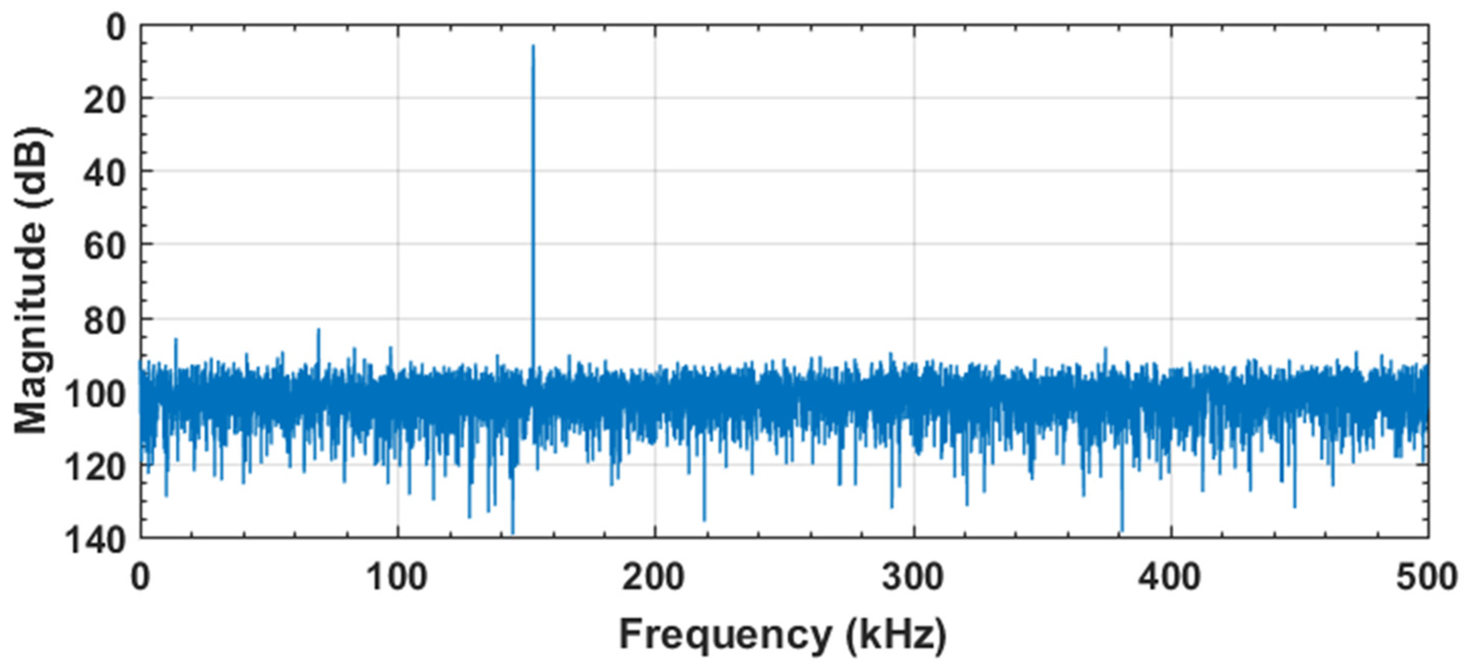
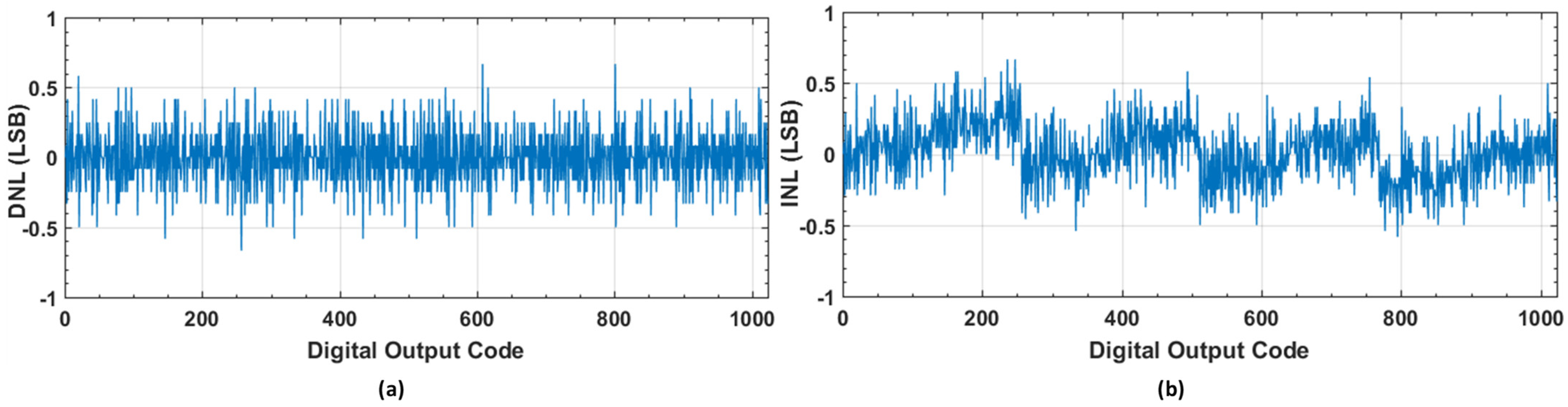
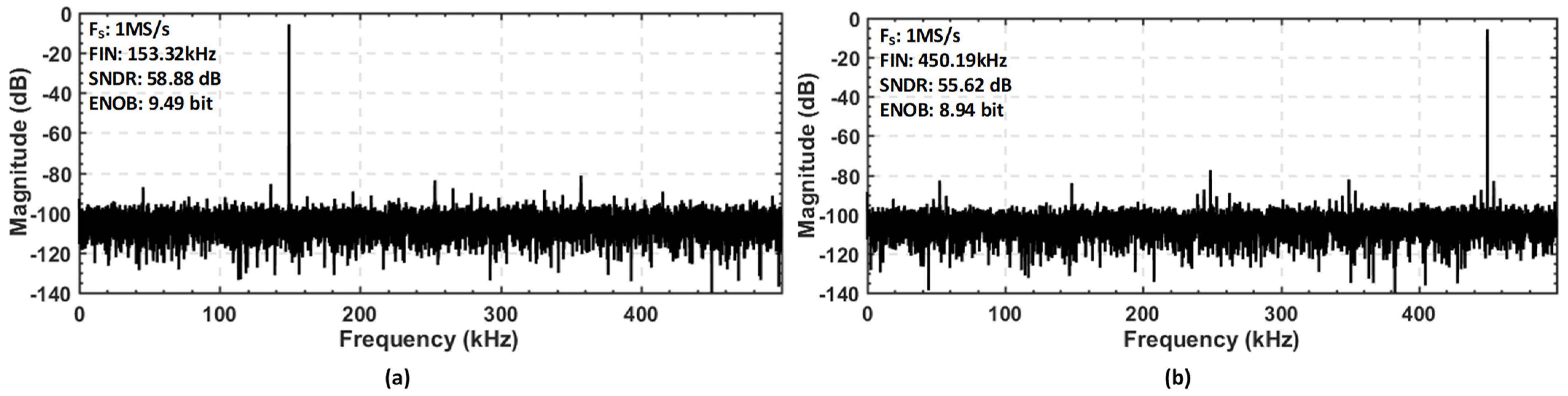
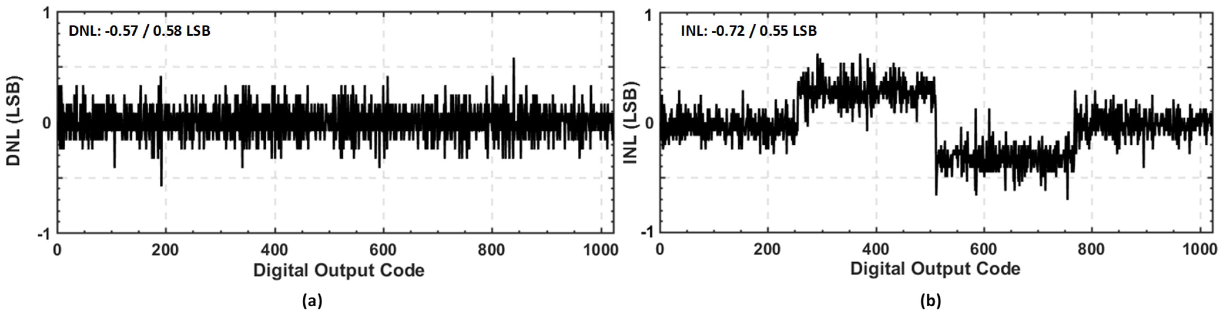
4. Measurement Results

The proposed SAR ADC architecture with VBGR was implemented and tested with TSMC 130 nm CMOS technology. Figure 13 represents a die photograph of the asynchronous SAR ADC with VBGR. The measured dynamic performance of the ADC at 153.32 kHz and 450.19 kHz input frequencies with a sampling rate of 1 MS/s is presented in Figure 14a,b, respectively. The proposed SAR ADC architecture achieved 9.49-bit ENOB and 58.88 dB SNDR with an input frequency of 153.32 kHz, as shown in Figure 14a, and 8.94-bit ENOB and SNDR of 55.62 db with an input frequency of 450.19 kHz at 1 MS/s sampling speed, as shown in Figure 14b.
To check the linearity or the static performance of the proposed SAR ADC, the measured DNL and INL results are presented in Figure 15. The measured DNL and INL were −0.57/0.58 LSB and −0.72/0.55 LSB, respectively. The ENOB trend of the proposed ADC with an on-chip EA-based bandgap reference voltage generator is depicted in Figure 16a,b, representing the power breakdown of the proposed EA-based bandgap reference voltage generator. Table 1 summarizes the performance of the proposed SAR ADC architecture and compares it with the other state-of-the-art SAR ADC architectures. The figure of Merit (FOM) is generally used to check the overall performance of ADC, and the FOM can be evaluated as below:
FOM = Power ADC min ( F S , 2 × BW ) 2 ENOB
where the sampling rate is presented as FS, bandwidth of ADC is denoted as BW, and power consumed by the proposed ADC is represented as PowerADC. The proposed SAR ADC architecture achieved a FOM of 66.25 fJ/conv-step.

5. Conclusions

A proposed prototype of a 10-bit 1 MS/s single-ended asynchronous SAR ADC with an on-chip bandgap reference voltage generator is fabricated with 130 nm technology. To optimize the power consumption, static, and dynamic performance several, techniques have been proposed. A dual-path bootstrap switch is proposed to increase the linearity sampling. The VCM-based CDAC switching technique has been implemented for the CDAC part to alleviate the switching energy problem of the capacitive DAC. The proposed architecture of the two-stage dynamic latch comparator provides high speed and low power consumption. Moreover, to achieve the faster bit conversion with an efficient time sequence, asynchronous SAR logic with an internally generated clock is implemented, which avoids the requirement for a high-frequency external clock, as all conversions are carried out in a single clock cycle. The proposed error amplifier-based bandgap reference voltage generator provides stable reference voltages to the ADC for practical implementation. The measurement results of the proposed SAR ADC including an on-chip bandgap reference voltage generator showed an ENOB of 9.49 bits and SNDR of 58.88 dB with 1.2 V of power supply and operation with a sampling rate of 1 MS/s.

Author Contributions

Conceptualization, D.V. and K.S.; methodology, D.V.; software, D.V., K.S. and S.J.K.; validation, D.V. and K.S.; formal analysis, D.V. and K.S.; investigation, D.V. and K.S.; resources, D.V.; data curation, D.V. and K.S.; writing—original draft preparation, D.V. and K.-Y.L.; writing—review and editing, D.V., Y.G.P., S.-S.Y. and K.-Y.L.; visualization, D.V., K.S. and K.-Y.L.; supervision, K.C.H., Y.Y. and K.-Y.L.; project administration, K.-Y.L. All authors have read and agreed to the published version of the manuscript.

Funding

This research received no external funding.

Institutional Review Board Statement

Not applicable.

Informed Consent Statement

Not applicable.

Data Availability Statement

Not applicable.

Acknowledgments

This paper was supported by Korea Institute for Advancement of Technology (KIAT) grant funded by the Korea Government (MOTIE) (P0012451, The Competency Development Program for Industry Specialist).

Conflicts of Interest

The authors declare no conflict of interest.

References

  1. Adeniran, O.A.; Demosthenous, A.; Clifton, C.; Atungsiri, S.; Soin, R. A CMOS low-power ADC for DVB-T and DVB-H systems. In Proceedings of the IEEE International Symposium Circuits and Systems (ISCAS), Vancouver, BC, Canada, 23–26 May 2004. [Google Scholar]
  2. Verma, D.; Rikan, B.S.; Shehzad, K.; Kim, S.J.; Khan, D.; Kommangunta, V.; Shah, S.A.A.; Pu, Y.; Yoo, S.-S.; Hwang, K.C.; et al. A Design of 44.1 fJ/Conv-Step 12-Bit 80 ms/s Time Interleaved Hybrid Type SAR ADC with Redundancy Capacitor and On-Chip Time-Skew Calibration. IEEE Access 2021, 9, 133143–133155. [Google Scholar] [CrossRef]
  3. Verma, D.; Kang, H.Y.; Shehzad, K.; Rehman, M.R.U.; Lee, K.-Y. Design of asynchronous SAR ADC for low power mixed signal applications. In Proceedings of the 2017 International SoC Design Conference (ISOCC), Seoul, Korea, 5–8 November 2017; pp. 222–223. [Google Scholar] [CrossRef]
  4. Van Elzakker, M.; Van Tuijl, E.; Geraedts, P.; Schinkel, D.; Klumperink, E.; Nauta, B. A 1.9μw 4.4fJ/Conversion-step10b1MS/s charge-redistribution ADC. In Proceedings of the 2008 IEEE International Solid-State Circuits Conference—Digest of Technical Papers, San Francisco, CA, USA, 3–7 February 2008; pp. 244–610. [Google Scholar]
  5. Verma, D.; Shehzad, K.; Kim, S.J.; Lee, K.Y. Low Power 10-BIT 8MS/s Asynchronous SAR ADC with Wake-up and Sample Logic for BLE Application. In Proceedings of the 2020 International Conference on Electronics, Information, and Communication (ICEIC), Barcelona, Spain, 19–22 January 2020; pp. 1–3. [Google Scholar] [CrossRef]
  6. Craninckx, J.; Van der Plas, G. A 65 fJ/conversion-step 0-to-50 MS/s 0-to-0.7 mW 9 b charge-sharing SAR ADC in 90 nm digital CMOS. In Proceedings of the 2007 IEEE International Solid-State Circuits Conference—Digest of Technical Papers, San Francisco, CA, USA, 11–15 February 2007; pp. 246–600. [Google Scholar]
  7. Shehzad, K.; Verma, D.; Khan, D.; Ain, Q.U.; Basim, M.; Kim, S.J.; Rikan, B.S.; Pu, Y.G.; Hwang, K.C.; Yang, Y.; et al. A Low-Power 12-Bit 20 MS/s Asynchronously Controlled SAR ADC for WAVE ITS Sensor Based Applications. Sensors 2021, 21, 2260. [Google Scholar] [CrossRef] [PubMed]
  8. Carusone, T.C.; Johns, D.A.; Martin, K.W. Analog Integrated Circuit Design; Wiley: New York, NY, USA, 2011. [Google Scholar]
  9. Gupta, M.S.; Oatley, J.L.; Joseph, R.; Wei, G.Y.; Brooks, D.M. Understanding voltage variations in chip multiprocessors using a distributed power-delivery network. In Proceedings of the Automation & Test in Europe Conference & Exhibition, Nice, France, 16–20 April 2007. [Google Scholar]
  10. Shehzad, K.; Verma, D.; Khan, D.; Ain, Q.U.; Basim, M.; Kim, S.J.; Pu, Y.; Hwang, K.C.; Yang, Y.; Lee, K.-Y. Design of a Low Power 10-b 8-MS/s Asynchronous SAR ADC with On-Chip Reference Voltage Generator. Electronics 2020, 9, 872. [Google Scholar] [CrossRef]
  11. Razavi, B. Design of Analog CMOS Integrated Circuits; McGraw Hill: New York, NY, USA, 2016. [Google Scholar]
  12. Osaki, Y.; Hirose, T.; Kuroki, N.; Numa, M. 1.2-V supply, 100-nW, 1.09-V bandgap and 0.7-V supply, 52.5-nW, 0.55-V sub bandgap reference circuits for nano watt CMOS LSIs. IEEE J. Solid-State Circ. 2013, 48, 1530–1538. [Google Scholar] [CrossRef]
  13. Verma, D.; Shehzad, K.; Khan, D.; Kim, S.J.; Pu, Y.G.; Yoo, S.-S.; Hwang, K.C.; Yang, Y.; Lee, K.-Y. A Design of Low-Power 10-bit 1-MS/s Asynchronous SAR ADC for DSRC Application. Electronic 2020, 9, 1100. [Google Scholar] [CrossRef]
  14. Lai, W.; Huang, J.; Lin, W. 1 MS/s low power successive approximations register ADC for 67-fJ/conversion-step. In Proceedings of the 2012 IEEE Asia Pacific Conference on Circuits and Systems, Kaohsiung, Taiwan, 2–5 December 2012; pp. 260–263. [Google Scholar]
  15. Liu, C.C.; Chang, S.J.; Huang, G.Y.; Lin, Y.Z.; Huang, C.M. A 1V 11fJ/conversion-step 10bit 10MS/s asynchronous SAR ADC in 0.18 μm CMOS. In Proceedings of the 2010 Symposium on VLSI Circuits, Honolulu, HI, USA, 16–18 June 2010; pp. 241–242. [Google Scholar]
  16. Yoshioka, K. VCO-Based Comparator: A Fully Adaptive Noise Scaling Comparator for High-Precision and Low-Power SAR ADCs. In IEEE Transactions on Very Large Scale Integration (VLSI) Systems; IEEE: Washington, DC, USA, 2021; Volume 29, pp. 2143–2152. [Google Scholar] [CrossRef]
  17. Saisundar, S.; Cheong, J.H.; Je, M. A 1.8 V 1 MS/s rail-to-rail 10-bit SAR ADC in 0.18μm CMOS. In Proceedings of the 2012 IEEE International Symposium on Radio-Frequency Integration Technology (RFIT), Singapore, 21–23 November 2012; pp. 83–85. [Google Scholar]
  18. Verma, D.; Shehzad, K.; Khan, D.; Ain, Q.U.; Kim, S.J.; Lee, D.; Pu, Y.G.; Lee, M.; Hwang, K.C.; Yang, Y.; et al. A Design of 8 fJ/Conversion-Step 10-bit 8MS/s Low Power Asynchronous SAR ADC for IEEE 802.15.1 IoT Sensor Based Applications. IEEE Access 2020, 8, 85869–85879. [Google Scholar] [CrossRef]
  19. Yoshioka, M.; Ishikawa, K.; Takayama, T.; Tsukamoto, S. A 10-b 50-MS/s 820-μW SAR ADC with On-Chip Digital Calibration. IEEE Trans. Biomed. Circuits Syst. 2021, 4, 410–416. [Google Scholar] [CrossRef] [PubMed]
  20. Chen, S.-W.M.; Brodersen, R.W. A 6-bit 600-MS/s 5.3-mW Asynchronous ADC in 0.13-μm CMOS. IEEE J. Solid-State Circ. 2006, 41, 2669–2680. [Google Scholar] [CrossRef]
  21. Banba, H.; Shiga, H.; Umezawa, A.; Miyaba, T.; Tanzawa, T.; Atsumi, S.; Sakui, K. A CMOS bandgap reference circuit with sub-1-Voperation. IEEE J. Solid-State Circ. 1999, 34, 670–674. [Google Scholar] [CrossRef] [Green Version]
  22. Ceekala, V.G.; Lewicki, L.D.; Wieser, J.B.; Varadarajan, D.; Mohan, J. A method for reducing the effects of random mismatches in CMOS bandgap references. In Proceedings of the 2002 IEEE International Solid-State Circuits Conference. Digest of Technical Papers (Cat. No. 02CH37315), San Francisco, CA, USA, 7 February 2002; pp. 318–319. [Google Scholar]
  23. Shehzad, K.; Kang, H.-Y.; Verma, D.; Park, Y.J.; Lee, K.-Y. Low-power 10-bit SAR ADC using class-AB type amplifier for IoT applications. In Proceedings of the 2017 International SoC Design Conference (ISOCC), Seoul, Korea, 5–8 November 2017; pp. 224–225. [Google Scholar]
  24. Wang, R.; Lu, W.; Zhao, M.; Niu, Y.; Liu, Z.; Zhang, Y.; Chen, Z. A sub-1ppm/°C current-mode CMOS bandgap reference with piecewise curvature compensation. IEEE Trans. Circuits Syst. I Regul. Pap. 2018, 65, 904–913. [Google Scholar] [CrossRef]
  25. Rad, R.E.; Hejazi, A.; Asl, S.-A.H.; Shehzad, K.; Verma, D.; Kim, S.; Rikan, B.S.; Pu, Y.; Kim, J.T.; Hwang, K.C.; et al. A 77-dB Dynamic-Range Analog Front-End for Fine-Dust Detection Systems with Dual-Mode Ultra-Low Noise TIA. Sensors 2021, 21, 6360. [Google Scholar] [CrossRef] [PubMed]
Figure 1. The proposed block diagram of the asynchronous SAR ADC with an EA-based bandgap reference voltage generator circuit.
Sensors 22 05393 g001
Figure 2. The schematic of the proposed bootstrap switch.
Sensors 22 05393 g002
Figure 3. The proposed 3-bit switching method for single-input SAR ADC.
Sensors 22 05393 g003
Figure 4. Dynamic performance of proposed switching with 1% unit capacitor mismatch.
Sensors 22 05393 g004
Figure 5. Static performance of the proposed switching with 1% unit capacitor mismatch. (a) DNL; (b) INL.
Sensors 22 05393 g005
Figure 6. Simulation result of capacitive DAC.
Sensors 22 05393 g006
Figure 7. Transistor-level schematic of the dynamic comparator.
Sensors 22 05393 g007
Figure 8. (a) Block diagram of the clock generator; (b) timing diagram of the clock generator.
Sensors 22 05393 g008
Figure 9. Schematic of variable delay cell.
Sensors 22 05393 g009
Figure 10. Schematic of BGR.
Sensors 22 05393 g010
Figure 11. (a) Detailed schematic of the proposed error amplifier based bandgap reference voltage generator; (b) Proposed folded-Cascoded error amplifier with intentional positive and negative feedback loop.
Sensors 22 05393 g011
Figure 12. Monte Carlo simulation result of error amplifier-based bandgap reference voltage generator.
Sensors 22 05393 g012
Figure 13. Die photograph of the asynchronous SAR ADC with VBGR.
Sensors 22 05393 g013
Figure 14. Measured dynamic performance at a sampling speed of 1 MS/s with the two different input frequencies: (a) 153.32 MHz input frequency; (b) 450.19 MHz input frequency.
Sensors 22 05393 g014
Figure 15. Measured static performance: (a) Differential non-linearity (DNL); (b) Integral non-linearity (INL).
Sensors 22 05393 g015
Figure 16. (a) Measured ENOB trend at different input frequencies with 1 MS/s sampling speed; (b) Power breakdown of proposed ADC.
Sensors 22 05393 g016
Table 1. Performance summary and comparison table.
Parameter[16][17][14][10][15]This Work
Technology (nm)6518018055180130
Resolution (bits) 13108101010
Supply Voltage (V)1.21.21.8111.2
Sampling Rate (MS/s)10118101
ENOB (bits)10.358.707.239.569.839.49
SNDR (dB)64.154.1345.359.360.9458.88
DNL (LSB)-0.40.66−0.2/0.4−0.3/0.2−0.57/0.58
INL (LSB)-0.460.61−0.6/0.5−0.3/0.2−0.72/0.55
Power Consumption (µW)98034.610.35729847.64
FOM (fJ/con-step)71836794.76366.25
Publisher’s Note: MDPI stays neutral with regard to jurisdictional claims in published maps and institutional affiliations.

