Article

Simple Fabrication of Photodetectors Based on MoS2 Nanoflakes and Ag Nanoparticles

1
College of BioNano Technology, Gachon University, Seongnam 13120, Korea
2
Department of Chemical Engineering, Ajou University, Suwon 16499, Korea
3
Department of Energy Systems Research, Ajou University, Suwon 16499, Korea
*
Authors to whom correspondence should be addressed.
Sensors 2022, 22(13), 4695; https://doi.org/10.3390/s22134695
Submission received: 20 May 2022 / Revised: 16 June 2022 / Accepted: 20 June 2022 / Published: 22 June 2022
(This article belongs to the Special Issue Advanced Materials for Sensing Applications)

Abstract

:
Low-dimensional transition-metal dichalcogenides (TMDs) have recently emerged as promising materials for electronics and optoelectronics. In particular, photodetectors based on mono- and multilayered molybdenum disulfide (MoS2) have received much attention owing to their outstanding properties, such as high sensitivity and responsivity. In this study, photodetectors based on dispersed MoS2 nanoflakes (NFs) are demonstrated. MoS2 NFs interact with Ag nanoparticles (NPs) via low-temperature annealing, which plays a crucial role in determining device characteristics such as good sensitivity and short response time. The fabricated devices exhibited a rapid response and recovery, good photo-responsivity, and a high on-to-off photocurrent ratio under visible light illumination with an intensity lower than 0.5 mW/cm2.

1. Introduction

Low-dimensional transition-metal dichalcogenides (TMDs) have received considerable attention as promising materials for high-performance semiconductors in several fields such as electronics, optoelectronics, and energy conversion and storage [1,2,3,4,5,6,7,8]. In particular, extensive research has been conducted to explore molybdenum disulfide (MoS2), which has a direct bandgap structure contributing to its excellent electrical and optical properties [9,10]. The fundamental properties of MoS2, such as quantum confinement effects and the functions of chalcogen vacancies and photoexcited carriers, have been extensively studied for their practical and potential applications [11,12,13,14,15]. Several electronic and optoelectronic devices, including field-effect transistors, charge-trap memories, and photodetectors based on mono- and multilayered MoS2, have been realized [16,17,18,19]. Interestingly, thin layers of MoS2 with structural integrity exhibit high light-absorption coefficients, enabling sensitive photon detection via photoexcited carriers. These thin layers are conventionally fabricated using chemical vapor deposition (CVD) growth methods [20,21,22]. Recently, solution-phase exfoliation and stabilization of TMDs have been proposed as alternative methods that facilitate facile and rapid fabrication [23,24,25,26]. These methods enable synthesis of MoS2 with small dimensions, such as nanoflakes (NFs), in a size-controlled manner, demonstrating their significant advantages such as low-temperature and solution-based processing. However, in the context of photodetecting, connectivity between MoS2 nanostructures with high light-absorption coefficients is required during film formation to provide conducting pathways for the collecting photoexcited carriers generated in MoS2 through electrodes. Thus, considerable research is underway to achieve high electrical conductivity and environmental stability in nanostructured MoS2 films. For example, band-selective photodetection has been successfully demonstrated using TMD nanosheets exfoliated with amine-terminated polymers in solution [27].
In this study, thin photodetectors based on dispersed MoS2 NFs are presented, and the optoelectronic properties for high absorption coefficients of photons are discussed in relation to experimental and theoretical studies. Initially, MoS2 NFs are synthesized in the solution phase with planar dimensions of ~20 nm for thin film formation via the drop-coating method, using Ag nanoparticles (NPs) formed from Ag nanofilms to ensure electrical connectivity between the MoS2 NFs. The Ag contacts to bulk MoS2 layers are known to become ohmic, and the resistivity of the MoS2 layers decreases after annealing at 400–600 °C [28]. Furthermore, Ag NPs and islands can enhance light absorption in photoresponsive devices via plasmonic [29,30]. Thus, the photoexcited carriers in MoS2 can be efficiently collected even under low-intensity illumination (<0.5 mW/cm2) with rapid response and recovery times. Photodetectors based on MoS2 NFs and Ag NPs have exhibited good photodetection abilities under low-intensity illumination and ambient conditions. This study provides a novel and simple route to achieve good performance thin photodetectors with desirable photodetection abilities for practical applications, particularly under low-intensity illumination conditions. These results demonstrate great potential for the development of advanced light-sensing systems, and other TMD-based applications such as transistors, memories, and energy conversion and storage devices.

2. Materials and Methods

2.1. Preparation of MoS2 NFs Solution

MoS2 NFs were prepared using a simple liquid exfoliation technique; 500 mg of MoS2 micro-crystals (Sigma Aldrich, St. Louis, MO, USA) were dispersed in 250 mL of a deionized (DI) water:ethyl alcohol (1:1) solution. The mixture was sonicated using a probe sonic tip (19 mm in diameter) at a power of 500 W using 10 s ON and 10 s OFF pulses for 10 h. DI water:ethyl alcohol solution (1:1, 50 mL) was added into the beaker every 2 h to maintain the volume of the MoS2 solution (250 mL) because the solution easily evaporated during ultrasonication owing to the high temperature. Additionally, the continuous feeding of the solution prevented a steep increase in temperature during the ultrasonication process. Subsequently, the solution was diluted to 1000 mL and centrifuged for 5 min at 5000 rpm to separate and remove the unexfoliated MoS2. The supernatant solution was further centrifuged at 8000 rpm for 30 min to remove large MoS2 particles. Approximately 90% of the supernatant solution was filtered under vacuum onto a membrane paper with a pore size of 100 nm. The filtered solution was dried in an oven to concentrate the MoS2 NF solution, until the volume of the solution reached 500 mL.

2.2. Photodetector Fabrication

Photodetectors were fabricated based on the schemes shown in Figure 1a. For example, the photodetector (20 nm Ag, 400 °C, vacuum, 24 h) exhibited high performance. In the typical procedure for the bottom-mode photodetector, a rectangular SiO2 (300 nm)/Si substrate with dimensions of 1 × 1 cm2 was cleaned using oxygen plasma equipment. The substrate was drop coated with the MoS2 NF solution at a solution/substrate ratio of ~0.3 mL/cm2. Subsequently, the solution was dried on the substrate in an oven at 80 °C for 30 min. The top Ag thin film was evaporated onto the sample under vacuum (<2 × 10⁻⁶ Torr) using a thermal evaporation system. The prepared sample was then annealed at 400 °C for 24 h in a muffle furnace at 1 atm, using a heating rate of 50 °C/min. After cooling to room temperature, the Au electrodes (50 nm) were evaporated onto the thin annealed film under vacuum using a patterned shadow mask. For the middle-mode photodetector, a 10 nm Ag layer was deposited on the SiO2 substrate and annealed at 400 °C for 24 h at atmospheric pressure. The MoS2 solution was then drop coated and dried in an oven at 80 °C for 30 min. A second 10 nm thick Ag film was deposited on the dried sample and annealed under the same conditions. Subsequently, the Au electrodes (50 nm) were evaporated onto the thin annealed film, as described above. An optical image of the fabricated device is shown in Figure 1c.

2.3. Process and Measurements

The following equipment was used: ultrasonicactor (SONICS-VCX500, SONICS, Newtown, CT, USA), centrifuge (UNIVERSAL 320R, Hettich, Beverly, MA, USA), field emission scanning electron microscope (FESEM, JSM-7500F, JEOL, Tokyo, Japan), vacuum muffle furnace (Neytech Qex, DEGUSSA-NEY DENTAL, INC., Bloomfield, CT, USA), light source (FOK-100W, Fiber Optic Korea, Cheonan, Korea), photodetectivity measurement system (4200-SCS, Keithley, Beaverton, OR, USA), thermal evaporation system, and solar simulator for the on/off test (XES-301S, SAN-EI ELECTRIC CO., Ltd., Osaka, Japan).

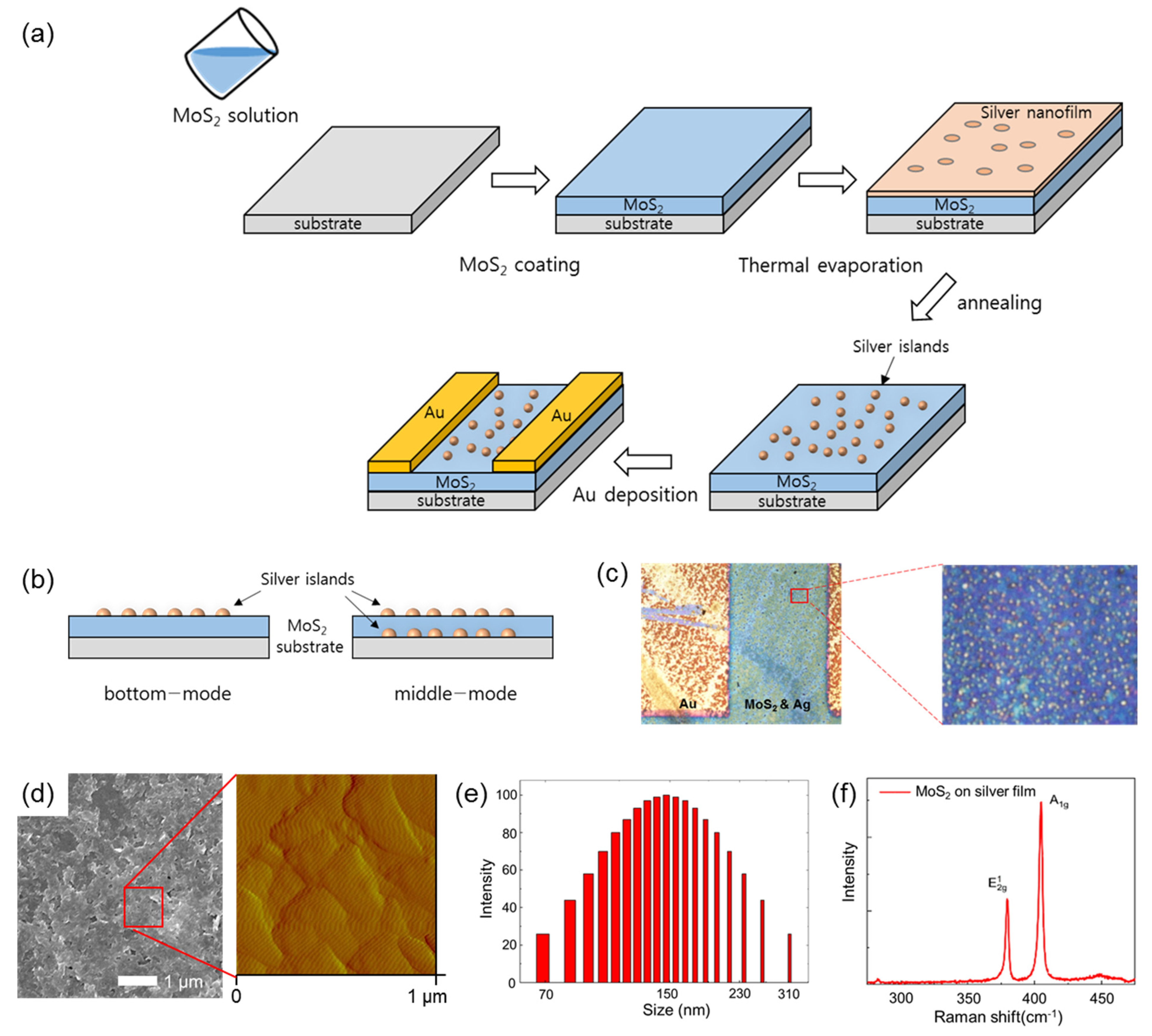
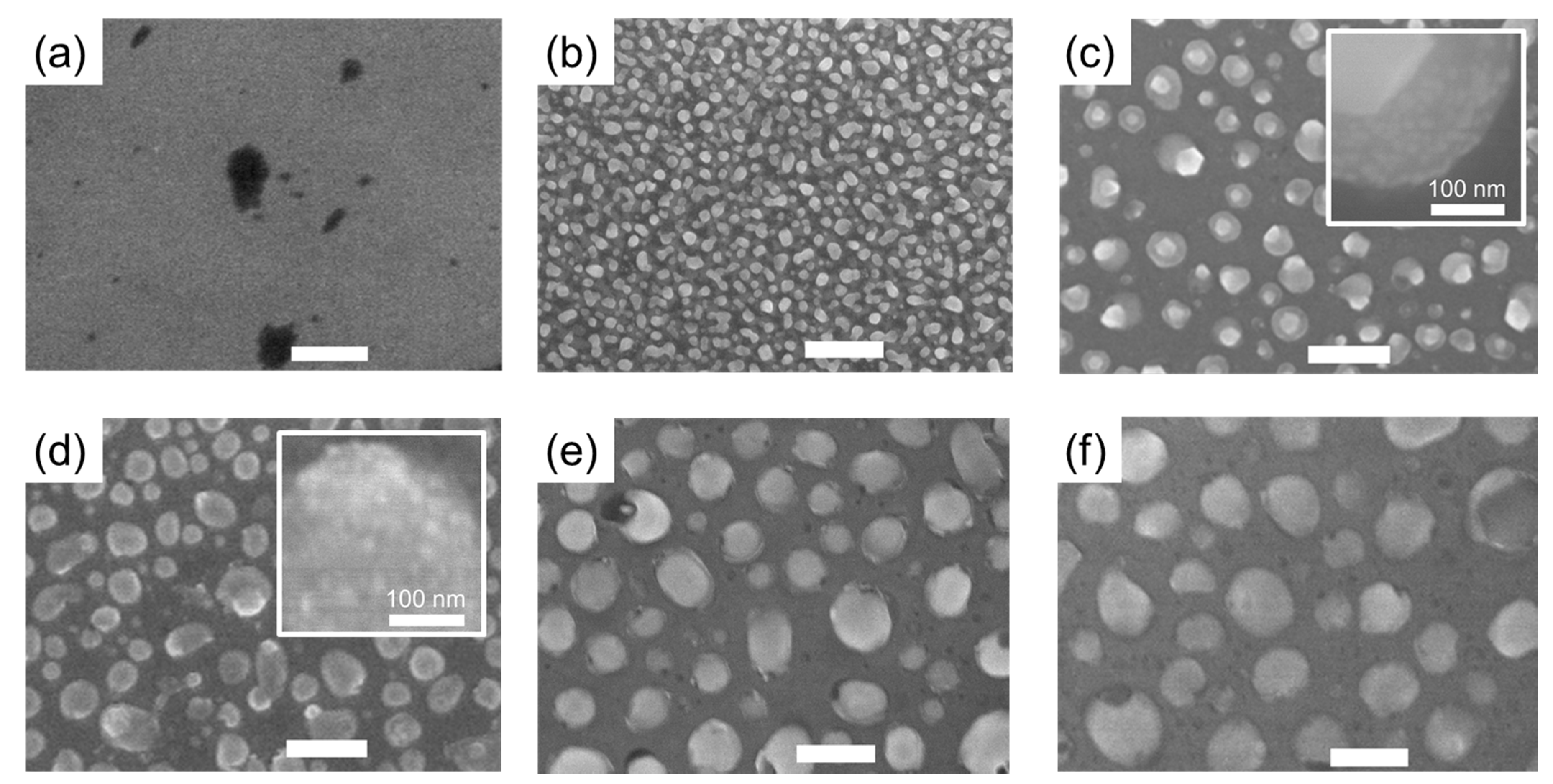
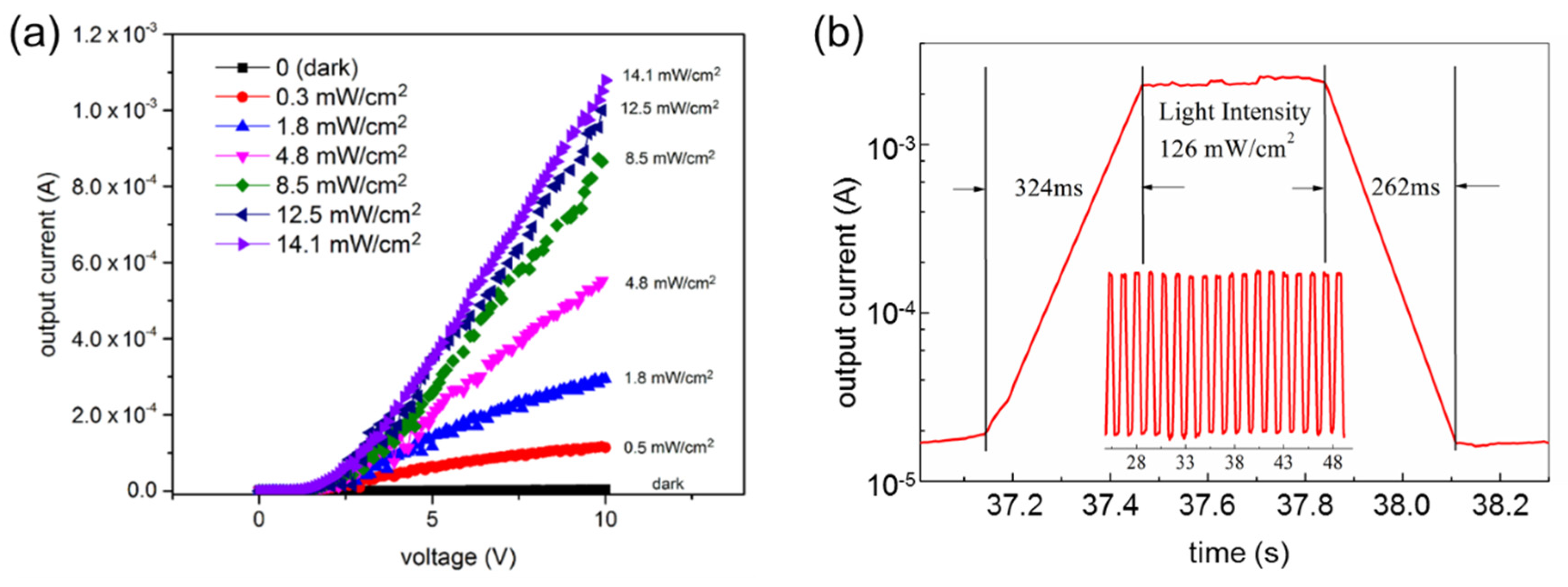
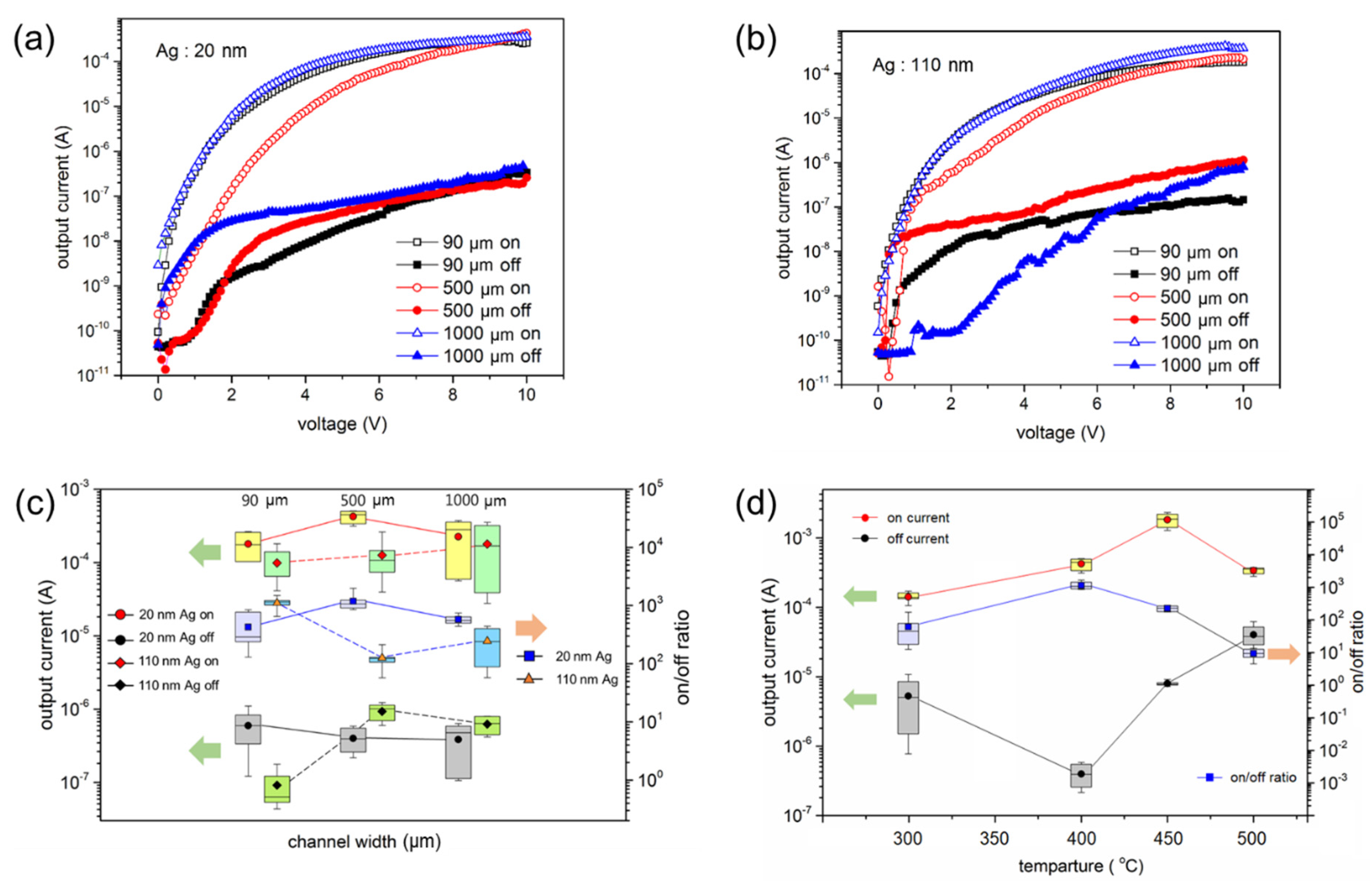
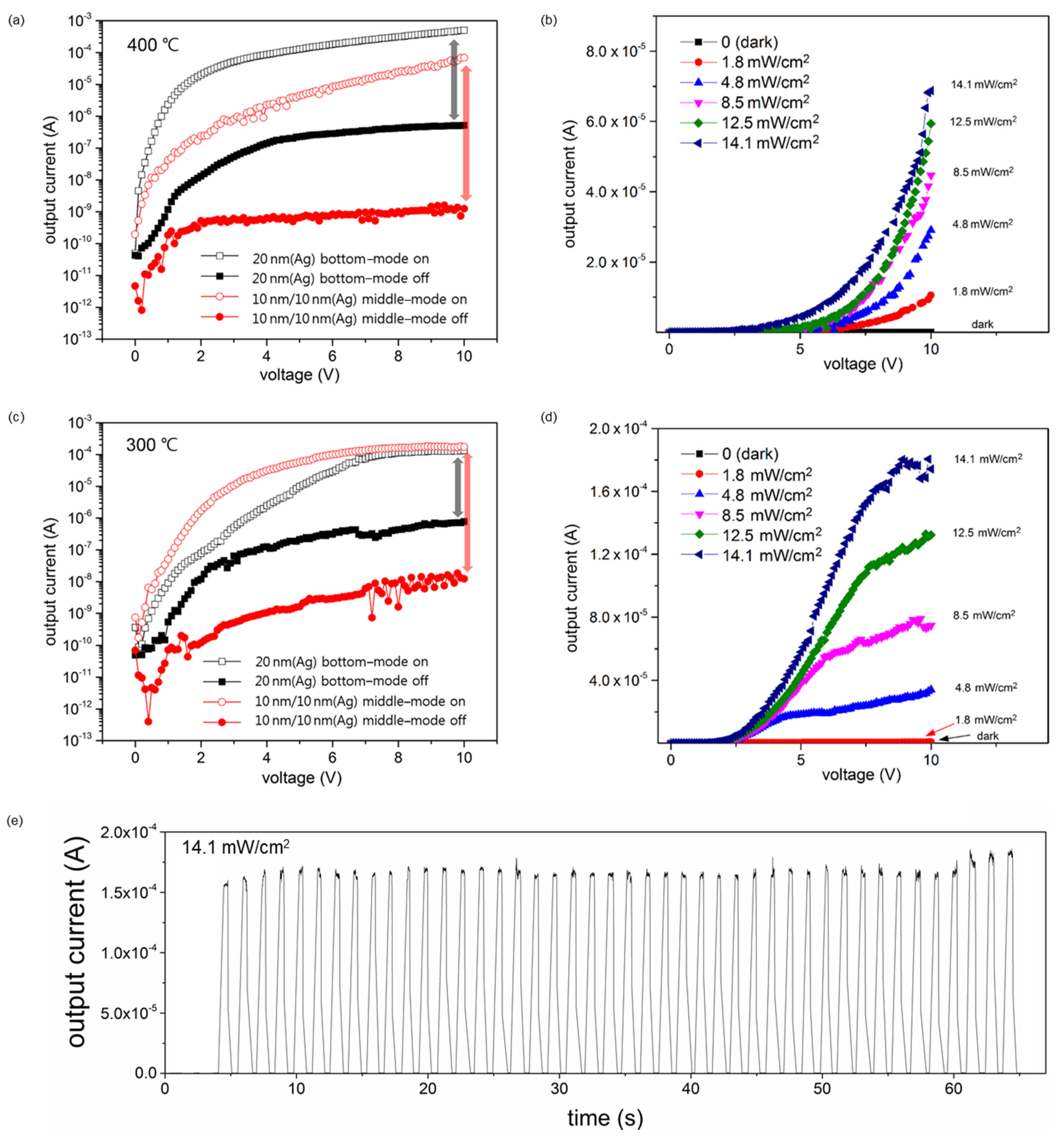
3. Results and Discussions

As the solvent of the MoS2 NFs solution was slowly evaporated, the MoS2 NFs were aggregated in a thin film form on the substrate. The surface morphology of the MoS2 film after solvent evaporation was examined as shown in Figure 1d. Scanning electron microscope (SEM) and atomic force microscopy (AFM) images clearly revealed that the MoS2 NFs were agglomerated, forming continuous domains. The thickness of the MoS2 film was measured to be ~20 nm, indicating the multilayered MoS2 domains. Size distribution of the MoS2 NFs in the solution is also shown in Figure 1e. Diameters of the NFs were mostly smaller than 300 nm, and it was also found that the most probable diameter of the NFs was 150 nm. In addition, Raman spectroscopy was employed to clarify the existence of the MoS2 NFs in the film without significant changes in chemical composition. Two prominent peaks were observed around 381 cm−1 and 409 cm−1, as shown in Figure 1f. These peaks can be assigned to the multilayered MoS2 in consideration of the peak shifts, which are typically observed in the multilayered MoS2. It is worth noting that the center of the thin film was not completely covered with the MoS2 NFs, due to the coffee-ring effect that occurred in the drop-casting process, and thus the substrate was partially exposed to air.
Figure 2 shows the SEM micrographs of the annealed Ag nanofilm on MoS2 layers at various temperatures (without annealing and annealed at 200, 400, 450, 500, and 550 °C). All samples were annealed for 24 h at atmospheric pressure. The surface of the Ag nanofilm (20 nm thick) on the MoS2 layer before the annealing process was flat, and some dark spots appeared on the surface, as shown in Figure 2a. The dark spots are slightly dented and considered to be an uncovered region of the MoS2 film. After annealing, the Ag film on MoS2 was dewetted and formed Ag islands on the surfaces, as shown in Figure 2b–f. Exfoliated MoS2 nanosheets are known to be electrically conductive [31]; however, the electrical conductivity of MoS2 films after the drop-coating process was low because there are many inter-nanosheet junctions between the MoS2 nanosheets, which complicates electron conduction between them at low voltages [32]. By annealing the Ag film, Ag diffused into the MoS2 layer, increasing the MoS2 conductivity. Furthermore, the contact between the metal and the MoS2 layer is known to become ohmic after diffusion, reducing the resistivity [33]. Thus, annealing of the Ag film improved the electrical contact between the MoS2 layers. In particular, the device, which was solely based on MoS2 without Ag, did not show any photo response. As mentioned above, this result is possibly originating from the inter-nanosheet junctions reducing the electrical conductivity. The MoS2 NFs were also concentrated at the edge of the thin film due to the coffee-ring effect in the drop-casting process, causing domain discontinuities near the center. Such disconnection between MoS2 disrupts the electron transportation and the photo response. However, when the Ag nanofilm was formed and annealed on the sample, the MoS2 domains were well connected to each other through the Ag islands consisting of the Ag NPs. The radii of the Ag islands were measured to be in the range of 10–600 nm, and the particle size increased with the annealing temperature (See Figure 2). It was also observed that small Ag NPs (<10 nm) were attached to the MoS2 surface, leading to connection between Ag and MoS2 after annealing. These results are consistent with the previous studies reporting that Ag can be easily attached to the MoS2 NFs. It has been reported that the Ag NPs can be attached to the MoS2 surface via the formation of the Ag ions in the solution [34], and the MoS2 layer can play a role as a photocatalyst with the Ag NPs [15]. Notably, the surface plasmon resonance effect of metal NPs can increase visible light absorption [35,36]. Surface plasmons can be localized by Ag NPs, and the excitation of localized surface plasmon resonance can occur. This leads to an enhanced electric field, which increases the photocurrent of the MoS2 layer.
Thin photodetectors based on MoS2 NFs and Ag NPs were fabricated as shown in Figure 1a. The two types of device structures, bottom-mode and middle-mode structures, are also described in Figure 1b. Prior to measuring performance of the Ag-coated MoS2 devices, a device with only the MoS2 film on the SiO2/Si substrate was fabricated that was annealed at various temperatures from 200 to 1000 °C in a muffle furnace. However, no photo response was observed in the device. Subsequently, two bottom-mode devices were fabricated with 20 and 110 nm thick Ag films. The Ag nanofilm on the MoS2 layer was annealed at 400 °C. The characteristic curves of the devices are shown in Figure 3a,b. Additionally, a device with a 200 nm Ag film was fabricated. However, the results for this device are not presented because the Ag layer was too thick, and Ag did not form islands after annealing. Thus, the device with a 200 nm Ag film short circuited and exhibited a maximum current of 1 × 10⁻² A at all voltages.
Subsequently, the channel width of the Au electrodes was varied from 90 to 1000 μm, as shown in Figure 3a,b. The characteristic current vs. voltage curves of the annealed device with the 20 nm Ag film are shown in Figure 3a, and those of the annealed device with the 110 nm Ag film are shown in Figure 3b. The devices were exposed under illumination using a visible light source (OSRAM, Munich, Germany, 64637) with a power density of 14.1 mW/cm2. All the devices were photoresponsive, and the devices were not strongly dependent on the channel width. As shown in Figure 3c, both devices with 20 and 110 nm Ag films show dark currents below 1 × 10⁻⁶ A and on-currents at 10 V over 1 × 10⁻⁴ A. Moreover, the on/off current ratios of the devices with 20 and 110 nm Ag films are shown in Figure 3c. The fabrication conditions (20 nm Ag film thickness and 500 μm channel width) showed the best performance and were adopted for further experiments. As shown in Figure 3d, the on/off ratio was affected the performance of the devices based on the annealing temperature conditions. The highest on-current at 10 V was observed for the device annealed at 450 °C. However, the off-current was also relatively higher than those of the devices annealed at 300 and 400 °C. Among them, the device annealed at 400 °C, which had the highest on/off ratio (1.66 × 10³), was selected for the fabrication process for better results in this study.
To evaluate the photodetection properties of the device annealed at 400 °C, the output characteristics and photoresponsivity were measured under visible light illumination with various intensities, as shown in Figure 4a. For the photoresponsive measurements, two sharp probes were brought into contact with the Au electrodes of the device. As mentioned previously, the device with 20 nm of Ag film and annealed at 400 °C showed the highest performance among the fabricated devices. Its photoresponsivity was 4.37 × 101 AW−1 under low-intensity illumination (~0.5 mW/cm2) and decreased to 1.53 × 101 AW−1 at a light intensity of 14.1 mW/cm2. The photocurrent gradually increased as the light intensity increased, and the photoresponsivity remained constant at ~1.5 × 101 AW−1. It is noteworthy that the photocurrent increased to ~11 mA at a sample bias voltage of 10 V under high-intensity illumination (14.1 mW/cm2). The time-resolved photo response of the device is shown in Figure 4b. The photocurrent of the device rapidly changed from 1.7 × 10⁻⁵ to ~2.5 × 10⁻³ A in response to the on/off switching of light illumination (126 mW/cm2) at a constant sample bias voltage of 10 V. The photo response and recovery times were consistently measured as ~324 and ~262 ms, respectively, because the on- and off-currents instantaneously returned to their initial levels without any losses. It is noteworthy that the shutter speed of the light source (a few milliseconds) was not compensated, and thus, the real response times were probably shorter than the measured values. The reversibility of the photoresponsive device is shown in the inset in Figure 4b. As the light illumination switches on and off, the initial off-current and on-current values are repeatedly obtained.
Based on the results, it was difficult to increase the on/off ratio above 2.0 × 10³ using the MoS2-Ag photoresponsive materials formed under the investigated conditions. Although the on-current of the device with a 10 nm thick Ag film was lower than that of the other fabricated devices with thicker Ag films, it exhibited a higher on/off ratio at 10 V compared with the other devices. Based on this result, another device configuration was evaluated to increase the on/off ratio. The middle-mode structure of the light-sensing device was designed, as shown in Figure 1b. To increase the light absorption of the device while maintaining a high on/off ratio, an Ag nanofilm was deposited and annealed before the MoS2 drop-coating process. This structure is called a ‘middle-mode’ structure, and the structure of previously discussed is called a ‘bottom-mode’ structure, as shown in Figure 1b. The designation of the structures was determined by the position of the MoS2 layer on the Ag films. In this study, the thickness of the Ag film below the MoS2 layer was 10 nm, and the same Ag film thickness was used for the device with the middle-mode structure. All Ag nanofilms of the devices were annealed immediately after deposition, as described previously. Particularly, the off-current of the device with 10 nm of Ag film annealed at 400 °C had a low value to be distinguished, compared with the devices with thicker Ag films. Thus, the middle-mode structure is suggested for increasing the on/off ratio of the photoresponsive device.
The characteristic curves of the two different devices annealed at 400 °C are shown in Figure 5a. The off-current of the bottom-mode device (Ag (20 nm)/MoS2/substrate) at a sample bias voltage of 10 V was relatively higher than the middle-mode device (Ag (10 nm)/MoS2/Ag (10 nm)/substrate), which was annealed at the same temperature. The device with the middle-mode structure showed a lower off-current, which resulted in a high on/off current ratio at 10 V. As shown in Figure 5b, the on-current of the middle-mode device under illumination with a visible light intensity of 14.1 mW/cm2 and a sample bias voltage of 10 V was 6.88 × 10⁻⁵ A, and the off-current under the same conditions was 1.25 × 10⁻⁹ A. Thus, the middle-mode device annealed at 400 °C exhibited low on- and off-current values, and the on/off current ratio was 5.61 × 10⁴ at 10 V, which is higher than that of the bottom-mode device with a 20 nm Ag film annealed at the same temperature. As shown in Figure 5b, the photocurrent of the middle-mode device gradually increased as the light intensity increased from 0 to 14.1 mW/cm2 at a sample bias voltage of 10 V. The photoresponsivity was 1.17 AW−1 under low-intensity illumination (~1.8 mW/cm2) and decreased to 9.75 × 10⁻¹ AW−1 at a light intensity of 14.1 mW/cm2.
Another device was fabricated under different annealing conditions to reduce the annealing temperature. The characteristic curves of the two different devices annealed at 300 °C are shown in Figure 5c. The off-current of the middle-mode device at a sample bias voltage of 10 V was lower than that of the bottom-mode device with a 20 nm Ag film annealed at 300 °C. The middle-mode device exhibited a higher on/off current ratio at a sample bias voltage of 10 V, compared with the bottom-mode device. As shown in Figure 5d, the on-current at a sample bias voltage of 10 V under illumination with a visible light intensity of 14.1 mW/cm2 was 1.74 × 10⁻⁴ A, and the off-current under the same conditions was 1.22 × 10⁻⁸ A. The middle-mode device annealed at 300 °C showed low on- and off-current values, and the on/off current ratio was 1.42 × 10⁴, which is 82.7 times higher than that of the bottom-mode device with a 20 nm Ag film annealed at 300 °C. The photocurrent of the middle-mode device at a sample bias voltage of 10 V gradually increased as the light intensity increased from 0 to 14.1 mW/cm2, as shown in Figure 5d. The photoresponsivity was 8.10 × 10⁻² AW−1 under low-intensity illumination (~1.8 mW/cm2) and increased to 2.47 AW−1 at a light intensity of 14.1 mW/cm2. Moreover, switching test was performed using the middle-mode device, of which the MoS2 film was sandwiched between the two Ag films (i.e., top and bottom). Each Ag film was 10 nm thick, and annealed at 300 °C. The device was repeatedly exposed to the visible light with an intensity of 14.1 mW/cm2 for 60 s. The current rapidly increased and decreased in response to the light as shown in Figure 5e. The device responded 43 cycles during 60 s, and the on-current was consistently maintained at ~1.6 × 10⁻⁴ A on average.
Based on these results, the on/off current of the device can be increased by fabricating a middle-mode structure and decreasing the annealing temperature to enhance the performance. Although the performance was not very high, the device annealed at 300 °C exhibited sufficient performance for application as a photoresponsive device. As reported in a previous study, Ag NPs located below the MoS2 layer enhanced the light absorption in the photoresponsive system [35]. In this study, a dewetted Ag film formed NPs on a MoS2 layer, which enhanced light absorption in the system. Thus, the dark current value was not significantly changed, and the on-current greatly increased owing to the enhanced light absorption by the Ag NPs below the active layer, resulting in an increase in the on/off ratio of the photoresponsive device.

4. Conclusions

Photodetectors were developed based on MoS2 NFs as the conversion center to transfer energy from photons to electrons in the thin film. In this study, after annealing, Ag diffused into the MoS2 layer, which decreased the resistance of the inter-nanosheet junctions between the MoS2 layers. Ag islands connected discontinuous MoS2 NFs each other. This increased the conductivity of the MoS2 layer. Moreover, the newly formed Ag islands on the MoS2 layer enhanced the absorption efficiency of light because the surface plasmon resonance effect of metal NPs increases visible light absorption. Two different device modes were fabricated for the photodetector. First, bottom-mode devices were fabricated to determine the optimal fabrication conditions based on performance. The bottom-mode device with a 20 nm Ag film annealed at 400 °C showed the highest performance, with a photoresponsivity of 4.37 × 101 AW−1 under low-intensity illumination (~0.5 mW/cm2) at a sample bias voltage of 10 V, and it exhibited the highest on/off ratio (1.66 × 10³). Second, a middle-mode device was fabricated to increase the on/off ratio. The middle-mode device annealed at 400 °C exhibited lower off-current, which caused a high on/off current ratio of 5.61 × 10⁴ at a sample bias voltage of 10 V. Therefore, the on/off ratio increased by over an order and was 82.7 times higher than that of the bottom-mode device annealed at 300 °C. In conclusion, MoS2 NFs play a major role in transferring newly generated electrons to the Ag film under illumination. Therefore, the developed methodology is proposed as an effective way to capture energy from conversion centers, such as TMD NFs using nano-thick metal films. This is a crucial concept for the utilization of various NFs and TMDs in optoelectronic applications. Thus, these results are expected to contribute to the advancement of high-performance photoresponsive systems for light-sensing applications.

Author Contributions

P.X.: conceptualization, methodology, formal analysis, investigation, data curation, visualization, and writing—original draft preparation; J.-H.K.: investigation, data curation, visualization, writing—original draft preparation, review and editing, and supervision; S.S.: conceptualization, formal analysis, visualization, writing—review and editing, supervision, and funding acquisition. All authors have read and agreed to the published version of the manuscript.

Funding

This work was supported by the Basic Science Research Program through the National Research Foundation of Korea (NRF-2021R1F1A1047036 and NRF-2018R1D1A1B07041253). This research was also supported by Korea Basic Science Institute (National research Facilities and Equipment Center) grant funded by the Ministry of Education (Grant No. 2020R1A6C101A184).

Institutional Review Board Statement

Not applicable.

Informed Consent Statement

Not applicable.

Data Availability Statement

Not applicable.

Conflicts of Interest

The authors declare no conflict of interest.

References

  1. Radisavljevic, B.; Radenovic, A.; Brivio, J.; Giacometti, V.; Kis, A. Single-layer MoS2 transistors. Nat. Nanotechnol. 2011, 6, 147–150. [Google Scholar] [CrossRef] [PubMed]
  2. Kim, S.; Konar, A.; Hwang, W.-S.; Lee, J.H.; Lee, J.; Yang, J.; Jung, C.; Kim, H.; Yoo, J.-B.; Choi, J.-Y.; et al. High-mobility and low-power thin-film transistors based on multilayer MoS2 crystals. Nat. Commun. 2012, 3, 1011. [Google Scholar] [CrossRef] [PubMed] [Green Version]
  3. Wang, H.; Yu, L.; Lee, Y.H.; Shi, Y.; Hsu, A.; Chin, M.L.; Li, L.-J.; Dubey, M.; Kong, J.; Palacios, T. Integrated circuits based on bilayer MoS2 transistors. Nano Lett. 2012, 12, 4674–4680. [Google Scholar] [CrossRef] [PubMed] [Green Version]
  4. Wang, K.; Wang, J.; Fan, J.; Lotya, M.; O’Neill, A.; Fox, D.; Feng, T.; Zhang, X.; Jiang, B.; Zhao, Q.; et al. Ultrafast saturable absorption of two-dimensional MoS2 nanosheets. ACS Nano 2013, 7, 9260–9267. [Google Scholar] [CrossRef]
  5. Ross, J.S.; Klement, P.; Jones, A.M.; Ghimire, N.J.; Yan, J.; Mandrus, D.G.; Taniguchi, T.; Watanabe, K.; Kitamuira, K.; Yao, W.; et al. Electrically tunable excitonic light-emitting diodes based on monolayer WSe2 p-n junctions. Nat. Nanotechnol. 2014, 9, 268–272. [Google Scholar] [CrossRef]
  6. Pospischil, A.; Furchi, M.M.; Mueller, T. Solar-energy conversion and light emission in an atomic monolayer p-n diode. Nat. Nanotechnol. 2014, 9, 257–261. [Google Scholar] [CrossRef]
  7. Stephenson, T.; Li, Z.; Olsen, B.; Mitlin, D. Lithium ion battery applications of molybdenum disulfide (MoS2) nanocomposites. Energy Environ. Sci. 2014, 7, 209–231. [Google Scholar] [CrossRef]
  8. Voiry, D.; Yamaguchi, H.; Li, J.; Silva, R.; Alves, D.C.; Fujita, T.; Chen, M.; Asefa, T.; Shenoy, V.B.; Eda, G.; et al. Enhanced catalytic activity in strained chemically exfoliated WS2 nanosheets for hydrogen evolution. Nat. Mater. 2013, 12, 850–855. [Google Scholar] [CrossRef]
  9. Splendiani, A.; Sun, L.; Zhang, Y.; Li, T.; Kim, J.; Chim, C.Y.; Galli, G.; Wang, F. Emerging photoluminescence in monolayer MoS2. Nano Lett. 2010, 10, 1271–1275. [Google Scholar] [CrossRef]
  10. Mak, K.F.; Lee, C.; Hone, J.; Shan, J.; Heinz, T.F. Atomically thin MoS2: A new direct-gap semiconductor. Phys. Rev. Lett. 2010, 105, 136805. [Google Scholar] [CrossRef] [Green Version]
  11. Lebègue, S.; Eriksson, O. Electronic Structure of Two Dimensional Crystals from ab Initio Theory. Phys. Rev. B 2009, 79, 115409. [Google Scholar] [CrossRef] [Green Version]
  12. Kuc, A.; Zibouche, N.; Heine, T. Influence of Quantum Confinement on the Electronic Structure of the Transition Metal Sulfide TS2. Phys. Rev. B 2011, 83, 245213. [Google Scholar] [CrossRef] [Green Version]
  13. Cheiwchanchamnangij, T.; Lambrecht, W.R. Band Structure Calculation of Monolayer, Bilayer, and Bulk MoS2. Phys. Rev. B 2012, 85, 205302. [Google Scholar] [CrossRef] [Green Version]
  14. Zeng, H.; Liu, G.B.; Dai, J.; Yan, Y.; Zhu, B.; He, R.; Xie, L.; Xu, S.; Chen, X.; Yao, W.; et al. Optical Signature of Symmetry Variations and Spin-Valley Coupling in Atomically Thin Tungsten Dichalcogenides. Sci. Rep. 2013, 3, 1608. [Google Scholar] [CrossRef] [Green Version]
  15. Daeneke, T.; Carey, B.J.; Chrimes, A.F.; Ou, J.Z.; Lau, D.W.M.; Gibson, B.C.; Bhaskaran, M.; Kalantar-Zadeh, K. Light driven growth of silver nanoplatelets on 2D MoS2 nanosheets templates. J. Mater. Chem. C 2015, 3, 4471–4478. [Google Scholar] [CrossRef]
  16. Mondal, B.; Som, A.; Chakraborty, I.; Baksi, A.; Sarkar, D.; Pradeep, T. Unusual reactivity of MoS2 nanosheets. Nanoscale 2016, 8, 10282–10290. [Google Scholar] [CrossRef]
  17. Liu, K.K.; Zhang, W.; Lee, Y.H.; Lin, Y.C.; Chang, M.T.; Su, C.Y.; Chang, C.-S.; Li, H.; Shi, Y.; Zhang, H.; et al. Growth of large-area and highly crystalline MoS2 thin layers on insulating substrates. Nano Lett. 2012, 12, 1538–1544. [Google Scholar] [CrossRef] [Green Version]
  18. Paur, M.; Molina-Mendoza, A.J.; Bratschitsch, R.; Watanabe, K.; Taniguchi, T.; Mueller, T. Electroluminescence from multi-particle exciton complexes in transition metal dichalcogenide semiconductors. Nat. Commun. 2019, 10, 1709. [Google Scholar] [CrossRef] [Green Version]
  19. Vella, D.; Barbosa, M.B.; Trevisanutto, P.E.; Verzhbitskiy, I.; Zhou, J.Y.; Watanabe, K.; Taniguchi, T.; Kajikawa, K.; Eda, G. In-Plane Field-Driven Excitonic Electro-Optic Modulation in Monolayer Semiconductor. Adv. Opt. Mater. 2022, 10, 2102132. [Google Scholar] [CrossRef]
  20. Zhan, Y.; Liu, Z.; Najmaei, S.; Ajayan, P.M.; Lou, J. Large-area vapor phase growth and characterization of MoS2 atomic layers on a SiO2 substrate. Small 2012, 8, 966–971. [Google Scholar] [CrossRef] [Green Version]
  21. Lim, Y.R.; Song, W.; Han, J.K.; Lee, Y.B.; Kim, S.J.; Myung, S.; Lee, S.S.; An, K.-S.; Choi, C.-J.; Lim, J. Wafer-Scale, Homogeneous MoS2 layers on Plastic Substrates for Flexible Visible-Light Photodetectors. Adv. Mater. 2016, 28, 5025–5030. [Google Scholar] [CrossRef] [PubMed]
  22. Golub, A.S.; Zubavichus, Y.V.; Slovokhotov, Y.L.; Novikov, Y.N. Single-layer dispersions of transition metal dichalcogenides in the synthesis of intercalation compounds. Russ. Chem. Rev. 2003, 72, 123–141. [Google Scholar] [CrossRef]
  23. Zheng, J.; Zhang, H.; Dong, S.; Liu, Y.; Tai Nai, C.; Suk Shin, H.; Jeong, H.Y.; Liu, B.; Ping Loh, K. High yield exfoliation of two-dimensional chalcogenides using sodium naphthalenide. Nat. Commun. 2014, 5, 2995. [Google Scholar] [CrossRef] [PubMed]
  24. Qiao, W.; Yan, S.; He, X.; Song, X.; Li, Z.; Zhang, X.; Zhong, W.; Du, Y. Effects of ultrasonic cavitation intensity on the efficient liquid-exfoliation of MoS2 nanosheets. RSC Adv. 2014, 4, 50981. [Google Scholar] [CrossRef]
  25. Coleman, J.N.; Lotya, M.; O’Neill, A.; Bergin, S.D.; King, P.J.; Khan, U.; Young, K.; Gaucher, A.; De, S.; Smith, R.J.; et al. Two-dimensional nanosheets produced by liquid exfoliation of layered materials. Science 2011, 331, 568–571. [Google Scholar] [CrossRef] [PubMed] [Green Version]
  26. Gan, Z.X.; Liu, L.Z.; Wu, H.Y.; Hao, Y.L.; Shan, Y.; Wu, X.L.; Chu, P.K. Quantum confinement effects across two-dimensional planes in MoS2 quantum dots. Appl. Phys. Lett. 2015, 106, 233113. [Google Scholar] [CrossRef]
  27. Velusamy, D.B.; Kim, R.H.; Cha, S.; Huh, J.; Khazaeinezhad, R.; Kassani, S.H.; Song, K.; Cho, S.H.; Hwang, I.; Lee, J.; et al. Flexible transition metal dichalcogenide nanosheets for band-selective photodetection. Nat. Commun. 2015, 6, 8063. [Google Scholar] [CrossRef] [Green Version]
  28. Souder, A.; Brodie, D.E. Electrical contacts and conductivity of MoS2 layer structures. Can. J. Phys. 1971, 49, 2565–2571. [Google Scholar] [CrossRef]
  29. Quan, J.; Zhang, J.; Qi, X.; Li, J.; Wang, N.; Zhu, Y. A study on the correlation between the dewetting temperature of Ag film and SERS intensity. Sci. Rep. 2017, 7, 14771. [Google Scholar] [CrossRef] [Green Version]
  30. Deng, Y.; Chen, M.; Zhang, J.; Wang, Z.; Huang, W.; Zhao, Y.; Nshimiyimana, J.P.; Hu, X.; Chi, X.; Hou, G.; et al. Thickness-dependent morphologies of Ag on n-layer MoS2 and its surface-enhanced Raman scattering. Nano Res. 2016, 9, 1682–1688. [Google Scholar] [CrossRef]
  31. Ogilvie, S.P.; Large, M.J.; Wood, H.J.; Graf, A.A.; Lee, F.; Salvage, J.P.; King, A.A.K.; Dalton, A.B. Size selection and thin-film assembly of MoS2 elucidates thousandfold conductivity enhancement in few-layer nanosheet networks. Nanoscale 2022, 14, 320–324. [Google Scholar] [CrossRef] [PubMed]
  32. Abraham, M.; Mohney, S.E. Annealed Ag contacts to MoS2 field-effect transistors. J. Appl. Phys. 2017, 122, 115306. [Google Scholar] [CrossRef]
  33. Schuller, J.A.; Barnard, E.S.; Cai, W.; Jun, Y.C.; White, J.S.; Brongersma, M.L. Plasmonics for extreme light concentration and manipulation. Nat. Mater. 2010, 9, 193–204. [Google Scholar] [CrossRef] [PubMed]
  34. Xiao, P.; Mencarelli, D.; Chavez-Angel, E.; Joseph, C.H.; Cataldo, A.; Pierantoni, L.; Torres, C.M.S.; Sledzinska, M. Reversing the Humidity Response of MoS2-and WS2-Based Sensors Using Transition-Metal Salts. ACS Appl. Mater. Interfaces 2021, 13, 23201–23209. [Google Scholar] [CrossRef] [PubMed]
  35. Ferry, V.E.; Verschuuren, M.A.; Li, H.B.; Verhagen, E.; Walters, R.J.; Schropp, R.E.; Atwater, H.A.; Polman, A. Light trapping in ultrathin plasmonic solar cells. Opt. Express 2010, 18, A237–A245. [Google Scholar] [CrossRef] [Green Version]
  36. Pan, R.; Kang, J.; Li, Y.; Zhang, Z.; Li, R.; Yang, Y. Highly Enhanced Photoluminescence of Monolayer MoS2 in Plasmonic Hybrids with Double-Layer Stacked Ag Nanoparticles. ACS Appl. Mater. Interfaces 2022, 14, 12495–12503. [Google Scholar] [CrossRef]
Figure 1. (a) Illustration of the fabrication of photodetecting devices. (b) Schematic of the bottom- and middle-mode structures. (c) Optical image of the fabricated device and magnified image of Ag islands on the MoS2 layer. (d) SEM image of MoS2 film and magnified AFM image of boxed area (e) Size distribution of the MoS2 NFs. (f) Raman spectra of MoS2 film on silver film.
Sensors 22 04695 g001
Figure 2. FESEM micrographs of annealed Ag nanofilms on the MoS2 layers at various temperatures. The thickness of the deposited Ag film was 20 nm. Samples were annealed at (a) room temperature (without annealing), (b) 200 °C, (c) 400 °C, (d) 450 °C, (e) 500 °C, and (f) 550 °C. The solid white bars represent the 1 μm length scale and the sold white bars in the inset of the (c,d) represent the 100 nm.
Sensors 22 04695 g002
Figure 3. Output characteristics (output current vs. sample bias voltage) of the bottom−mode photodetecting devices under various fabricating conditions: (a) 20 nm and (b) 110 nm Ag films annealed at 400 °C with various electrode channel widths (90, 500, and 1000 μm). Output currents were measured under visible light illumination with an intensity of 14.1 mW/cm2 (on) and 0.0 mW/cm2 (off). (c) Output currents and on/off ratios of bottom−mode devices in (a,b) at a bias voltage of 10 V. (d) Output currents and on/off ratios at a bias voltage of 10 V of the bottom−mode devices with a 500 µm electrode channel width and 20 nm Ag film thickness annealed at various temperatures (300, 400, 450, and 500 °C).
Sensors 22 04695 g003
Figure 4. (a) Output characteristics of the bottom−mode photodetecting device with 20 nm of Ag film annealed at 400 °C with a 500 μm electrode channel width. Output currents were measured under visible light illumination with various intensities of 0.0 (dark), 0.5, 1.8, 4.8, 8.5, 12.5, and 14.1 mW/cm2. (b) Real-time characteristics of the output current measured in response to a light intensity of 14.1 mW/cm2 at a constant sample bias voltage of 10 V. The data clearly show the reversible photoresponsivity of the device.
Sensors 22 04695 g004
Figure 5. (a) Output characteristics of the bottom-mode device with 20 nm (top) of Ag film and middle-mode device with 10 nm (top)/10 nm (bottom) of Ag film, both annealed at 400 °C. (b) Output characteristics of the middle-mode device with 10 nm (top)/10 nm (bottom) of Ag film annealed at 400 °C under visible light illumination with various intensities. (c) Output characteristics of the bottom-mode device with 20 nm (top) of Ag film and middle-mode device with 10 nm (top)/10 nm (bottom) of Ag film, both annealed at 300 °C. (d) Output characteristics of the middle-mode device with 10 nm (top)/10 nm (bottom) of Ag film annealed at 300 °C under visible light illumination with various intensities. The on and off-currents of (a,c) were measured under visible light illumination with an intensity of 14.1 mW/cm2. The output currents of (b,d) were measured under visible light illumination with various intensities of 0.0 (dark), 1.8, 4.8, 8.5, 12.5, and 14.1 mW/cm2. (e) Switching test curve of the middle-mode device with 10 nm (top)/10 nm (bottom) of Ag film annealed at 300 °C. The device responded 43 cycles for 60 s under visible light illumination with an intensity of 14.1 mW/cm2.
Sensors 22 04695 g005
Publisher’s Note: MDPI stays neutral with regard to jurisdictional claims in published maps and institutional affiliations.

