1. Introduction
CdZnTeSe (CZTS) material has been under development for hard X-ray and gamma-ray semiconductor detectors [
1,
2,
3]. It was observed that the addition of Se to the CdZnTe (CZT) matrix provides improved compositional homogeneity and mitigates many performance-limiting defects [
4]. The CZTS material exhibits comparable or even better electrical and spectroscopic properties as CdTe and CZT materials [
1,
5,
6,
7,
8,
9,
10].
CdTe-based detectors can be annealed in different atmospheres to improve the electrical and spectroscopic properties. Low-temperature annealing is typically performed on CdTe-based materials in the temperature range of 370–520 K. Studies investigating the influence of low-temperature annealing on CdTe/CdZnTe material have reported controversial results [
11,
12,
13,
14,
15]. However, these studies were performed on samples with planar electrodes, which do not allow the investigators to distinguish between bulk and surface leakage currents. This is necessary for separating the change in metal/semiconductor interface and surface conditions. Our recent study demonstrated the influence of low-temperature annealing on the surface leakage current and bulk current, especially on the Schottky barrier height [
16]. The sample was treated with temperatures between 313 K up to 373 K in ambient air.
Another method used to change the detector properties of CdTe-based materials is electromigration. Here, the charged defects drift in an external electric field. Kim et al. [
17] showed the improvement in the mobility-lifetime product after the treatment of CZT at 493 K at a voltage of 60 V for 7 and 60 days, which they assigned to the electromigration of Cu, Fe, and Ga impurities. Additional studies demonstrated the electromigration of positively charged donors in CdTe-based materials, which mainly affect the electrical properties [
18,
19,
20].
In this article, we provide the results of the annealing of CZTS performed at standard operating conditions of detectors to analyze their potential impact on the material and contact characteristics. We performed low-temperature annealing in the temperature range of 320 K to 360 K with an applied bias of V. We focused on the changes in the electric field distributions and I–V characteristics at room temperature after finishing each annealing step under bias. We observed that low-temperature annealing causes an increase in the barrier height at the contacts that, in general, limits the dark current and decreases the positive space charge present in the sample before annealing.
2. Materials and Methods
We studied a CZTS sample with Se and Zn. The sample was cut from a CZTS ingot, which was grown by the traveling heater method with doping of In in the ppm range. The sample dimensions were mm. AlO abrasive was used to mechanically polish the sample surface (surface RMS 2 nm) without any further chemical treatment. The metal electrodes were evaporated on the large opposite sides. One contact was planarly made from indium. The opposite gold contact consisted of a guard ring and a central electrode, which allowed us to separate the bulk and surface leakage currents. The area of the central electrode was . It was separated from the guard ring electrode covering the rest of the surface by a 500 µm wide gap.
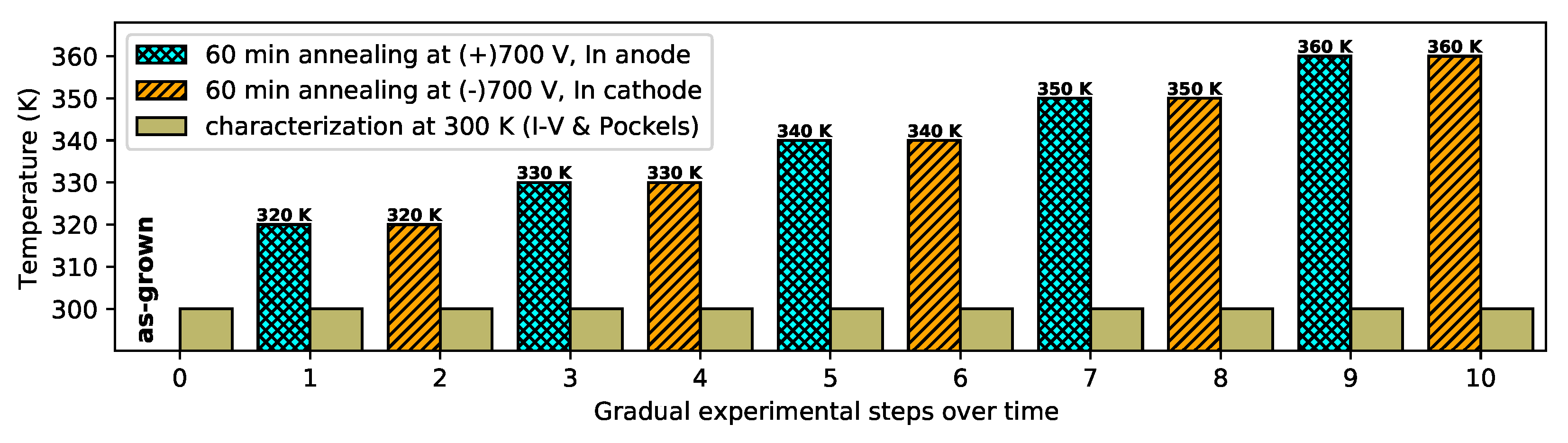
For low-temperature annealing of the CZTS and its characterization, the sample was mounted in an optical cryostat equipped with fine temperature regulation using a Peltier device. An argon atmosphere was maintained in the cryostat at all times. The setup allowed the characterization of the sample between annealing steps without any further manipulation. Before annealing, the as-grown sample was characterized by I–V and electric field (Pockels) measurements (step 0). Each annealing step was conducted in the following way: the sample temperature was stabilized to the required value. Then, a bias of 700 V (with the respective polarity of the indium electrode) was applied for 60 min using a Keithley 2410 source meter. Individual annealing steps were performed for both voltage polarities. The temperature of the annealing steps was increased by 10 K in the range of 320–360 K. Electronic properties were measured after each step at 300 K. A scheme of gradual experimental steps over time is shown in
Figure 1.
For the characterization at 300 K, the CZTS sample was biased by a Keithley 2410 source meter, and I–V curves were measured by two Keithley 2000 multimeters (bulk and leakage currents) in the range of
. The distributions of internal electric fields between electrodes were measured by a standard cross-polarizers technique using the electro-optic Pockels effect for the CZTS crystal, which has a
m symmetry [
21]. This method allows evaluating a spatial distribution of the internal electric field
of a biased sample at
from the relative transmittance distribution
measured using low-intensity light (LED at 1550 nm) and an infrared InGaAs CMOS camera. Here,
is the passed light intensity distribution of the biased sample with perpendicular polarizers, and
is the passed light intensity distribution of the sample at zero bias with parallel polarizers. Then,
.
3. Results and Discussion
The analysis of the influence of low-temperature annealing under bias on the CZTS detector is based on the study of changes in the total space charge, profiles of the internal electric fields, and I–V curves between individual annealing steps.
3.1. Electric Field and Space Charge
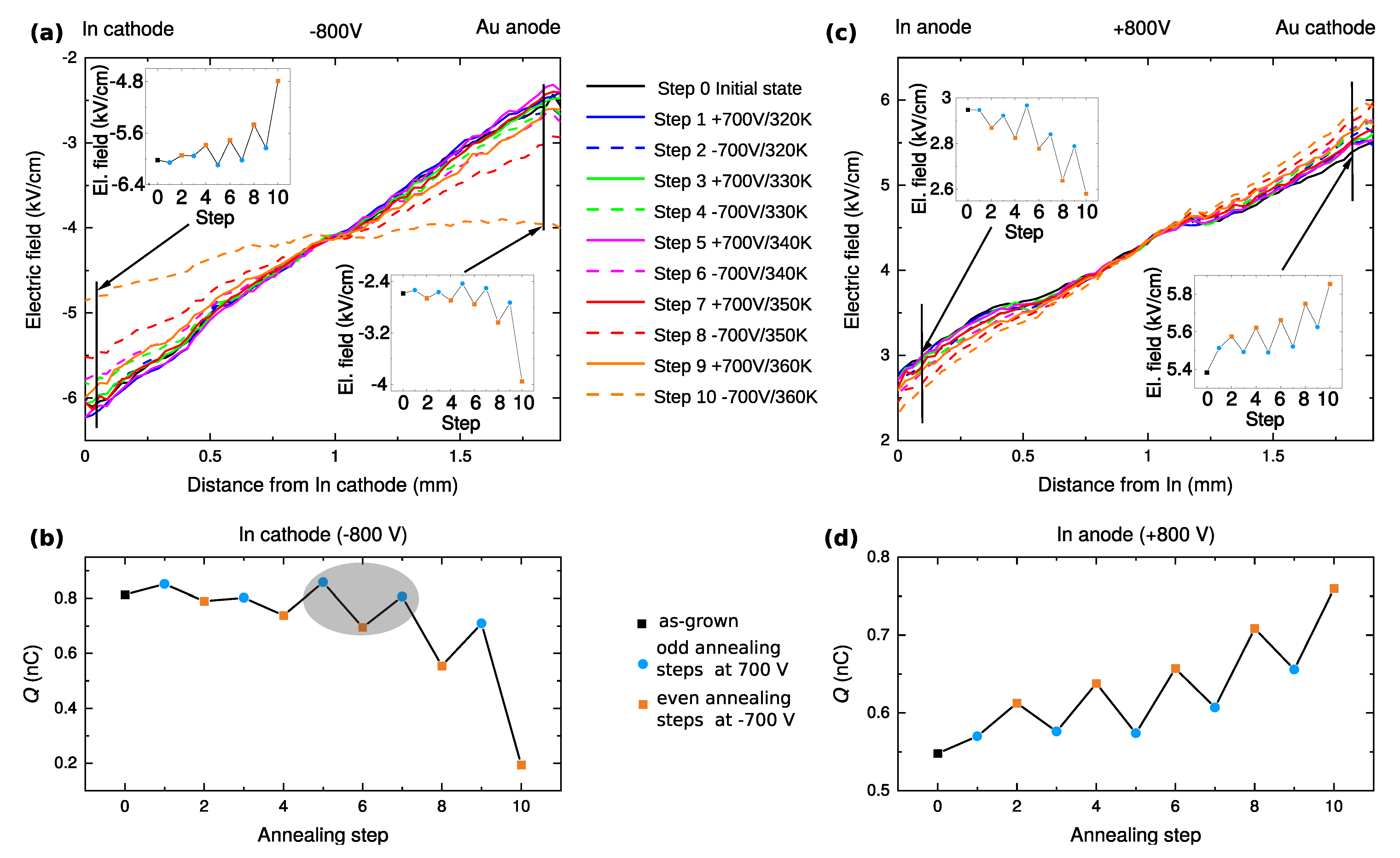
The internal electric field distributions measured after each annealing step are depicted in
Figure 2a,c for
V and
V, respectively. Here, and in all other cases, the polarity is always related to the indium electrode, i.e., the positive/negative polarity means that the indium contact is anode/cathode. The total space charge
Q was calculated from the electric field distribution [
22] as
, where
is the permittivity,
S is the electrode area, and
and
are the electric field amplitudes at the cathode and the anode, respectively. The corresponding total space charge for each step and both polarities is shown in
Figure 2b,d.
In the as-grown sample, the absolute value of the electric field (black solid line) decreases from the cathode to the anode for both polarities. It testifies to the presence of a positive space charge in the sample (black square in
Figure 2b,d). The positive space charge remains in the sample after all annealing steps. However, its absolute value is changing.
Focused on the electric-field profiles and the space charge measured with negative polarity on the indium electrode (cathode) shown
Figure 2a,b, respectively, the gradual annealing treatment resulted in a decrease in the positive space charge when compared to the as-grown state (from
C to
C, which corresponds to the charge density
throughout the sample). There are considerable saw-tooth dependencies in
Figure 2(a-insets),b that indicate a significant effect of the bias polarity during the annealing on the space charge. Here, the total space charge induced by annealing at negative and positive polarity forms the lower and upper envelope of its dependence shown in
Figure 2b, respectively.
In the case of opposite polarity (In anode,
Figure 2c), we observed the opposite effect of the applied bias at annealing on the values of the positive space charge (the blue circles follow a lower envelope line compared with the red squares in
Figure 2d, which is an opposite behavior compared to
Figure 2b). Furthermore, the positive total space charge at room temperature grew with the annealing steps. The electric field profile can be well approximated using a linear function in all cases reflecting a nearly constant distribution of the space charge in the volume of the sample.
In summary, the profiles of the internal electric field and the total space charge density evaluated at room temperature are influenced by both the temperature and polarity of the applied bias during annealing.
3.2. I–V Measurements
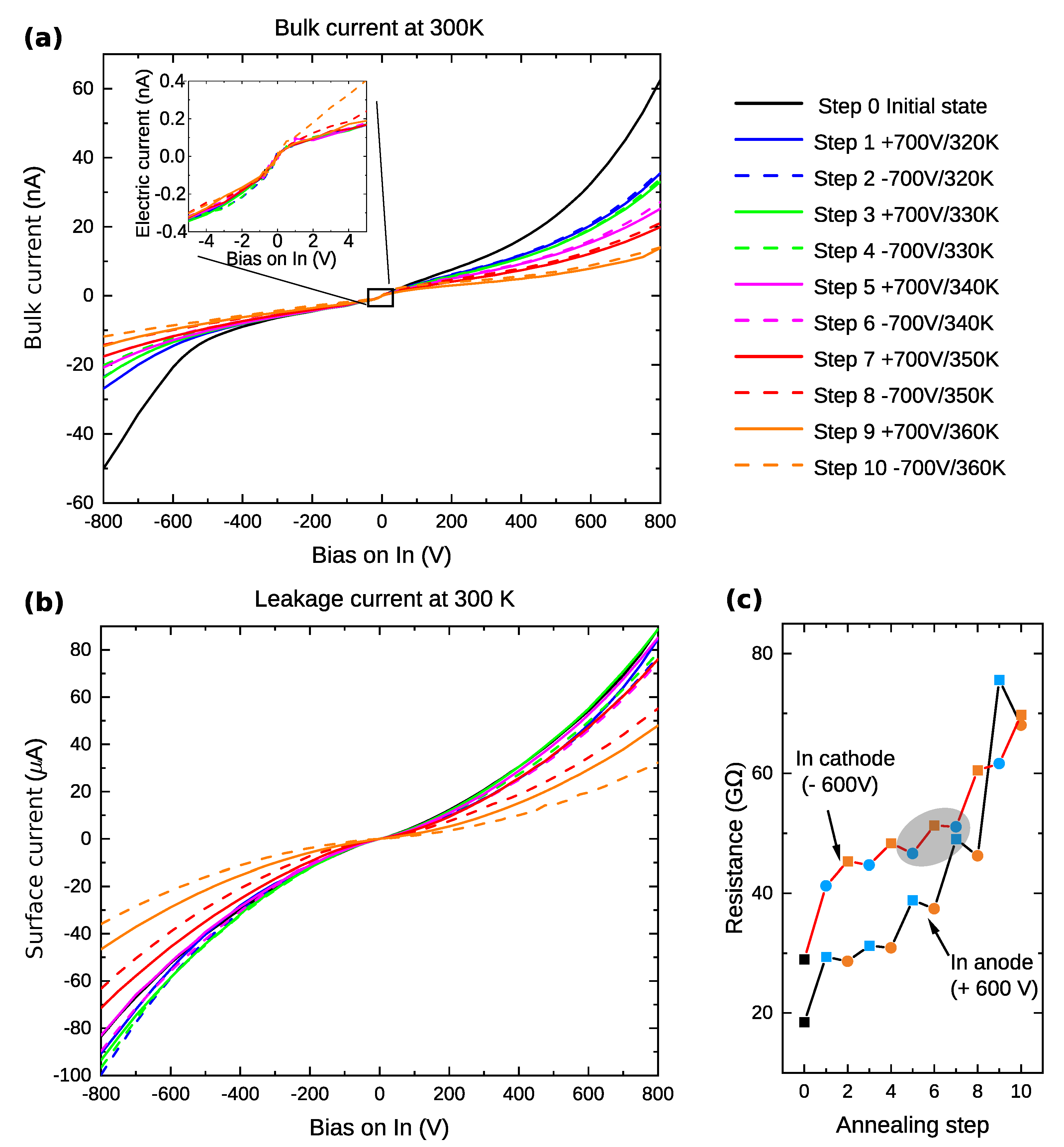
The I–V characteristics at room temperature after each annealing step are shown in
Figure 3. The bulk current and leakage surface currents were measured separately.
Let us focus now on the bulk current, which is presented in
Figure 3a. Firstly, we analyzed the material bulk specific resistivity
from the I–V characteristics around 0 V (inset of
Figure 3a) using Ohm’s law
, where
S is the contact area and
l is the distance between contacts. The calculated sample’s specific resistivity depicted in
Figure 4 shows a decrease with increasing annealing temperature. This decrease is smaller when the In contact is positively biased during annealing. After the final annealing step at 360 K (
V), the specific resistivity slightly decreased to
cm from its initial value of
cm before the first annealing step.
When the bias is increased above approx.
V in both polarities (inset of
Figure 3a), the slope of the I–V characteristics is smaller than at biases around 0 V. The characteristic has an S-shape character, indicating the depletion of free carriers in the bulk.
It is apparent that the resistance at high biases strongly depends on the applied annealing step. We specifically chose the resistance at
V (
Figure 3c) for further analysis and development of the model explaining the experimental data.
3.3. Physical Model
The most-important experimental results plotted in
Figure 2 and
Figure 3 are summarized in
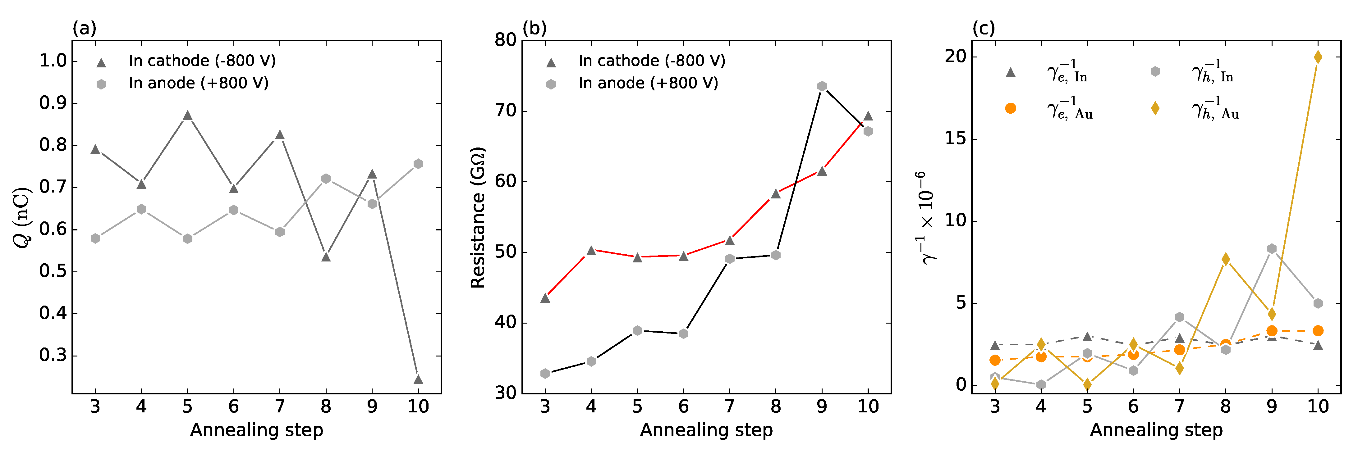
Table 1, which shows the evolution of the space charge and resistance
of the sample (evaluated at
V) induced by the annealing step. Double and single arrows correspond to the large and small change, respectively. We can identify the important correlation of the charge and resistance changes. When the resistance grows, the space charge decreases. When the resistance slightly decreases, the space charge increases. For the explanation of these phenomena, we must analyze the mechanisms responsible for the sample’s charging.
In semi-insulating semiconductors, both electrons and holes participate in the transport. The positive space charge formed in the biased semiconductor may be, in general, induced either by an injecting anode or a blocking cathode. Injecting an anode is increasing the concentration of holes that can be trapped at deep levels. This way a positive space charge in the bulk can be formed. Another possibility to form a positive space charge is to use a blocking cathode. In this case, electrons are depleted in the bulk, and an uncompensated fixed space charge is present in the volume of the sample. In our case, we may reject the injection of holes. The I–V characteristics displayed in
Figure 3a clearly show the S-character proving the blocking contact. Moreover, the almost perfectly linear profiles of the electric field in
Figure 2 sign the charging by carrier depletion. On the other hand, the carrier injection would produce curves deviating from linear profiles as predicted by the theory of the Space Charge Limited Currents [
23,
24]. Consequently, the blocking cathode may be considered as the primary attribute responsible for the positive space charge formation in the sample before annealing—step 0. Since the same features are observed for both positive and negative biasing, we may conclude that both contacts, Au and In, act in the same way.
Let us now focus on the evolution of the resistance and space charge with the annealing steps—
Figure 2c,d and
Figure 3c and
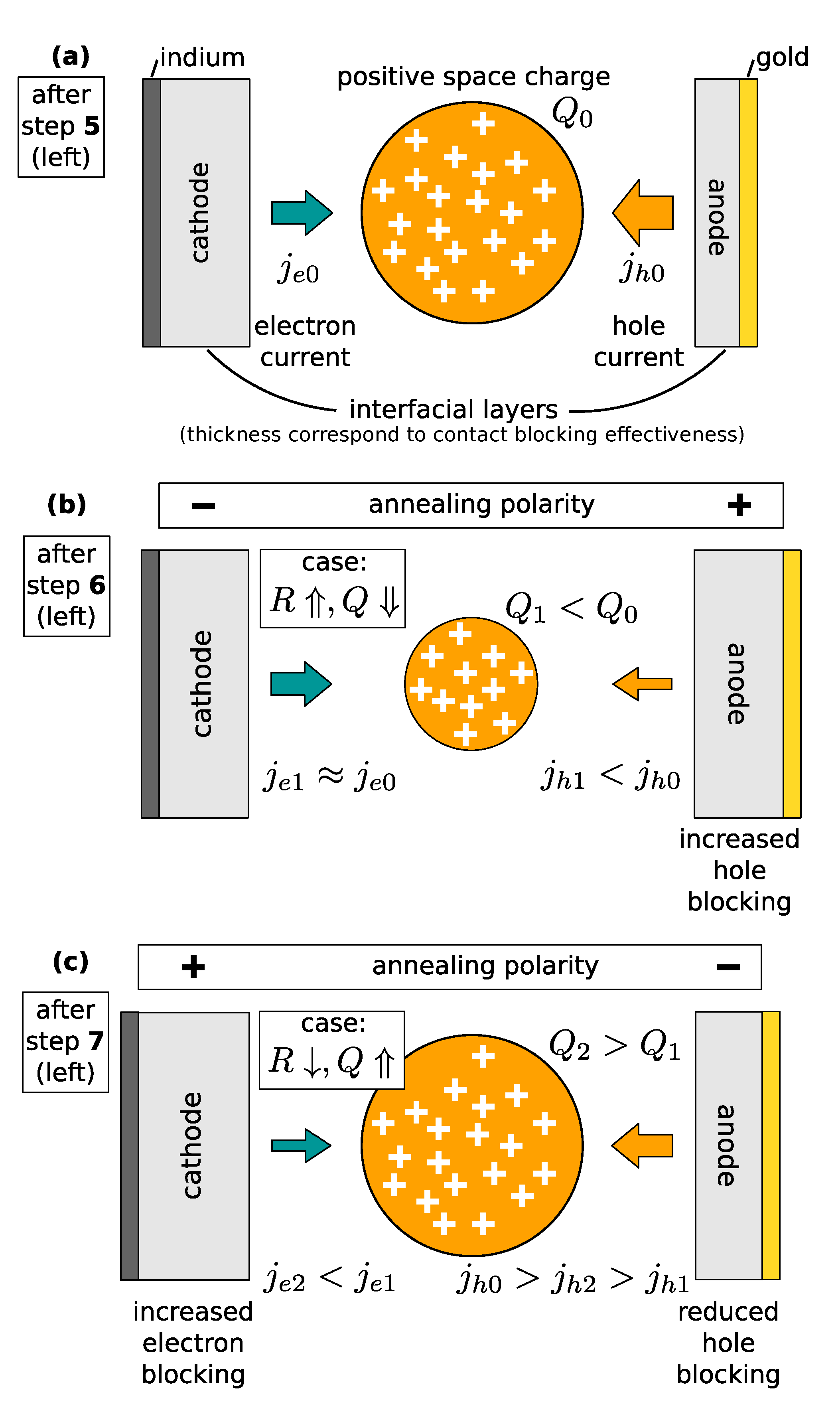
Table 1. We can see that the annealing steps resulting in the resistance increase are accompanied by a space charge reduction. This situation may be then unambiguously explained as the enhancement of the blocking character of the anode inducing the hole depletion. The electrical current is smaller and the resistance is higher due to the reduction of the hole component. At the same time, a smaller hole current results in a smaller hole trapping at deep levels. This way the positive space charge in the bulk is reduced. A scheme representing the above-mentioned processes is shown in
Figure 5.
Figure 5a,b represent the conditions in the sample after annealing steps 5 and 6, respectively. A scheme representing the processes leading to this situation is presented as a change between
Figure 5a,b that represents the conditions in the sample after annealing steps 5 and 6, respectively.
The interpretation of the effect of the annealing steps resulting in the increase in the positive space charge is more complex. The increased cathode blocking or reduced anode blocking may result in the desired effect. That would, however, contradict the observed nearly unchanged specific resistivity evaluated from the slopes of the I–V characteristics at a bias close to 0—
Figure 4. We thus conclude that this situation can be explained by the parallel activity of both mechanisms when the increased resistance caused by enhanced cathode blocking is compensated by reduced resistance due to lowered anode blocking. A scheme describing this situation is presented in
Figure 5c, and it corresponds to the effect of annealing step no. 7.
3.4. Numeric Simulations
We tested the validity of the presented physical model by numerical simulation illustrating the oscillatory character of the charge and resistance shown in
Figure 2b,d and
Figure 3c, respectively. The calculations were done with the homemade code [
23,
25] solving the drift-diffusion and Poisson’s equations. We defined the defect structure of the bulk by trial parameters: Fermi energy
eV, one electron trap with the density
cm
localized below
at the energy
eV, and one hole trap above
with the density
cm
at the energy
eV. Since we investigated only the steady state here, the respective capture cross sections cannot be determined [
23]. The effect of the annealing was simulated by tuning transfer rates
defining the source of carriers in both contacts [
23]. We used flat bands at the simulations since the information on the band bending is not accessible. Besides, the respective band bending may be compensated by appropriate tuning of the transfer rates so that it does not disable the simulation.
Defining the source of the charge on contacts through the transfer rates represents the simplest option to introduce the model of contact barriers to the theory. It allows us to easily demarcate the maximum particular current conforming simultaneously to the zero electric current at zero bias. Evidently, a realistic model of contacts would have to be described by a much more complex theory. For such specification, we do not have enough experimental data, and the detailed contact properties investigation was not the primary aim of the research. The visualization of the fitted is more convenient in the inverted form since it corresponds to the blocking character of the interface barriers.
We plot in
Figure 6a,b the results of the simulations of the charge and resistance, respectively. It is seen that the evolution of both quantities truly depicts the experimental data in
Figure 2b,d. Corresponding inverted transfer rates
are presented in
Figure 6a. We can see that, in agreement with the suggested model, the polarization is more ruled by the evolution of barriers blocking holes (solid connecting lines). In case of electrons, the effect is less distinctive (dashed connecting lines). Nevertheless, the evolution of barriers blocking electrons has a dominant effect on the space charge tuning. In the negative electric field (see
Figure 2b), the electron barrier at the In contact remains stable, and the ascending barrier of holes on Au leads to the reduction in the polarization. Oppositely, the electron barrier on Au contact grows similarly as the hole barrier at the In contact, which results in the stable polarization in spite of the enhanced resistance of the detector. Although the fit shows weak deviations from the experiment, the principal features were undoubtedly depicted. The better fit would need a comprehensive optimization involving both the defect structure and the surface barrier parameters.
3.5. Interpretation
The effects of low temperature annealing up to 360 K of the biased semi-insulating CZTS can be summarized as the following: The bulk material resistivity remains practically unchanged, while major changes affecting the electronic properties of the detector, such as the total space charge and dark current at high voltage bias (therefore, the resistance at
) under which the detectors work by default, are associated with the development of surface states under the electrodes. During annealing, when the particular electrode is positive, its ability to block both types of carriers increases. If the electrode during annealing is negative, its ability to block holes decreases, while its ability to block electrons does not change. Observed changes show signs of universality because the effects do not depend on whether the electrode is indium or gold. By suitable tuning and a combination of conditions of low-temperature annealing under bias (temperature and polarity) and polarity used during the detector operation, its resistance can be significantly increased, and the effect of positive-space-charge accumulation on the traps can be reduced. In addition, it appears advantageous to anneal the sample at a temperature of at least 350 K, at which there is a significant reduction in the surface current, as can be seen in
Figure 3b.
We assumed that the modification of the barriers at the contacts after low-temperature annealing could be explained by the development of an insulation layer between the semiconductor and metal electrodes. The difference between an expected I–V behavior based on the work function model and our observations can be attributed to a thin interfacial layer between the semiconductor and metallic electrodes. Although there is no source of oxygen during the annealing and characterisation processes, we expect the presence of a-few-nm thick oxide (TeO
) layer at the CZTS surface before contact deposition, which could slightly develop (change its thickness vs. concentration) during annealing and therefore affect the barrier’s electronic properties. We reported the initial presence of a 2.8 nm thick TeO
layer at the CZTS surface with a concentration of 66% recently in the [
16] estimated by ellipsometry measurements and analysis performed on the sample with the similar surface treatment. If there is a significantly thick interfacial layer with a reasonably high density of states, the Fermi level is pinned by the surface states, and the barrier height is independent of the metal workfunction, and it is given by the surface properties as mentioned in the [
26].
4. Conclusions
We investigated the influence of low-temperature annealing under an applied bias on the basic electrical properties of the detector-grade material CdZnTeSe. We treated the CZTS sample with temperatures in the range where detectors normally work from 320 K to 360 K, and with a normal detector bias voltage ( V). We measured the internal electric field profiles and I–V characteristics after each annealing step. We observed that the profiles of the internal electric field and the total space charge density evaluated at room temperature are influenced by both the temperature and polarity of the applied bias during annealing. We analyzed the I–V characteristics measured at room temperature after each annealing step and evaluated the specific resistivity of the bulk and resistance at V. We could identify correlations between the charge and resistance changes. We explained the experimental data by a qualitative model based on the modification of the contact barriers by annealing. Low-temperature annealing of the contacts under bias can be used to modify the contact properties.
Author Contributions
M.R., V.D. and J.F. proposed the idea of the annealing of CZTS detector under bias. M.R. and V.D. discussed the experimental aspects of the used methods. M.R. conducted the annealing and characterizing experiments and analyzed them, and he was the lead author for the original manuscript. R.G. was the main author of the qualitative physical model with contributions by J.F. and V.D. Co-authors U.N.R. and R.B.J. provided expertise to grow and prepare the CdZnTeSe crystal used in the experiments. All authors contributed to the preparation of the manuscript. All authors have read and agreed to the published version of the manuscript.
Funding
This research received no external funding.
Institutional Review Board Statement
Not applicable.
Informed Consent Statement
Not applicable.
Data Availability Statement
Data collected through the research presented in the paper are available on request from the first and the corresponding authors.
Acknowledgments
This work was supported by the Grant Agency of the Czech Republic project 19-17783S. This work was also partially supported by the U.S. Department of Energy, Office of Defense Nuclear Nonproliferation Research and Development, and the Laboratory Directed Research and Development (LDRD) program within the Savannah River National Laboratory (SRNL) and the DOE Minority Serving Institution Partnership Program (MSIPP).
Conflicts of Interest
The authors declare no conflict of interest.
References
- Gul, R.; Roy, U.N.; Camarda, G.S.; Hossain, A.; Yang, G.; Vanier, P.; Lordi, V.; Varley, J.; James, R.B. A comparison of point defects in CdZnTeSe crystals grown by Bridgman and traveling heater methods. J. Appl. Phys. 2017, 121, 125705. [Google Scholar] [CrossRef]
- Roy, U.N.; Camarda, G.S.; Cui, Y.; Gul, R.; Yang, G.; Zazvorka, J.; Dedic, V.; Franc, J.; James, R.B. Evaluation of CdZnTeSe as a high-quality gamma-ray spectroscopic material with better compositional homogeneity and reduced defects. Sci. Rep. 2019, 9, 7303. [Google Scholar] [CrossRef] [PubMed] [Green Version]
- Roy, U.N.; Camarda, G.S.; Cui, Y.; Gul, R.; Hossain, A.; Yang, G.; Zazvorka, J.; Dedic, V.; Franc, J.; James, R.B. Role of selenium addition to CdZnTe matrix for room-temperature radiation detector applications. Sci. Rep. 2019, 9, 1620. [Google Scholar] [CrossRef] [PubMed] [Green Version]
- Roy, U.N.; Camarda, G.S.; Cui, Y.; Yang, G.; James, R.B. Impact of selenium addition to the cadmium-zinc-telluride matrix for producing high energy resolution X-and gamma-ray detectors. Sci. Rep. 2021, 11, 10338. [Google Scholar] [CrossRef] [PubMed]
- Roy, U.N.; Camarda, G.S.; Cui, Y.; James, R.B. High-resolution virtual Frisch grid gamma-ray detectors based on as-grown CdZnTeSe with reduced defects. Appl. Phys. Lett. 2019, 114, 232107. [Google Scholar] [CrossRef]
- Roy, U.N.; Camarda, G.S.; Cui, Y.; Gul, R.; Yang, G.; James, R.B. Charge-transport properties of as-grown Cd1-xZnxTe1-ySey by the traveling heater method. AIP Adv. 2018, 8, 125015. [Google Scholar] [CrossRef] [Green Version]
- Egarievwe, S.U.; Roy, U.N.; Agbalagba, E.O.; Harrison, B.A.; Goree, C.A.; Savage, E.K.; James, R.B. Optimizing CdZnTeSe Frisch-Grid Nuclear Detector for Gamma-Ray Spectroscopy. IEEE Access 2020, 8, 137530–137539. [Google Scholar] [CrossRef]
- Egarievwe, S.U.; Roy, U.N.; Harrison, B.A.; Goree, C.A.; Savage, E.K.; Jones, J.; James, R.B. Fabrication and Characterization of CdZnTeSe Nuclear Detectors. In Proceedings of the 2019 IEEE Nuclear Science Symposium and Medical Imaging Conference (NSS/MIC), Manchester, UK, 26 October–2 November 2019. [Google Scholar] [CrossRef]
- Rejhon, M.; Franc, J.; Dedic, V.; Pekarek, J.; Roy, U.N.; Grill, R.; James, R.B. Influence of deep levels on the electrical transport properties of CdZnTeSe detectors. J. Appl. Phys. 2018, 124, 235702. [Google Scholar] [CrossRef] [Green Version]
- Rejhon, M.; Dedic, V.; Beran, L.; Roy, U.N.; Franc, J.; James, R.B. Investigation of Deep Levels in CdZnTeSe Crystal and Their Effect on the Internal Electric Field of CdZnTeSe Gamma-ray Detector. IEEE Trans. Nucl. Sci. 2019, 66, 1952–1958. [Google Scholar] [CrossRef]
- Mergui, S.; Hage-Ali, M.; Koebel, J.M.; Siffert, P. Thermal annealing of gold deposited contacts on high resistivity p-type CdTe nuclear detectors. Nucl. Instrum. Methods Phys. Res. Sect. Accel. Spectrom. Detect. Assoc. Equip. 1992, 322, 375–380. [Google Scholar] [CrossRef]
- Wang, L.; Sang, W.; Shi, W.; Qian, Y.; Min, J.; Liu, D.; Xia, Y. Electrical properties of contacts on P-type Cd0.8Zn0.2Te crystal surfaces. Nucl. Instrum. Methods Phys. Res. Sect. Accel. Spectrom. Detect. Assoc. Equip. 2000, 448, 581–585. [Google Scholar] [CrossRef]
- Kim, K.H.; Hwang, S.; Fochuk, P.; Nasi, L.; Zappettini, A.; Bolotnikov, A.E.; James, R.B. The Effect of Low-Temperature Annealing on a CdZnTe Detector. IEEE Trans. Nucl. Sci. 2016, 63, 2278–2282. [Google Scholar] [CrossRef]
- Ozaki, T.; Iwase, Y.; Takamura, H.; Ohmori, M. Thermal treatment of CdTe surfaces for radiation detectors. Nucl. Instrum. Methods Phys. Res. Sect. Accel. Spectrom. Detect. Assoc. Equip. 1996, 380, 141–144. [Google Scholar] [CrossRef]
- Park, S.H.; Ha, J.H.; Lee, J.H.; Kim, H.S.; Cho, Y.H.; Kim, Y.K. Effect of Thermal Annealing on the Metal-Semiconductor Contact of a CZT Schottky Detector. J. Korean Phys. Soc. 2009, 55, 2378–2382. [Google Scholar] [CrossRef]
- Rejhon, M.; Franc, J.; Zazvorka, J.; Dedic, V.; Kunc, J. Influence of low-temperature annealing on Schottky barrier height and surface electrical properties of semi-insulating CdTe. Semicond. Sci. Technol. 2017, 32, 085007. [Google Scholar] [CrossRef]
- Kim, K.; Kim, S.; Hong, J.; Lee, J.; Hong, T.; Bolotnikov, A.E.; Camarda, G.S.; James, R.B. Purification of CdZnTe by electromigration. J. Appl. Phys. 2015, 117, 145702. [Google Scholar] [CrossRef] [Green Version]
- Belas, E.; Grill, R.; Bugar, M.; Prochazka, J.; Hlidek, P.; Praus, P.; Franc, J.; Hoschl, P. Electromigration of Mobile Defects in CdTe. IEEE Trans. Nucl. Sci. 2009, 56, 1752–1757. [Google Scholar] [CrossRef]
- Elhadidy, H.; Grill, R.; Franc, J.; Šik, O.; Moravec, P.; Schneeweiss, O. Ion electromigration in CdTe Schottky metal–semiconductor–metal structure. Solid State Ionics 2015, 278, 20–25. [Google Scholar] [CrossRef]
- Elhadidy, H.; Grill, R.; Franc, J.; Moravec, P.; Musiienko, A.; Dědič, V.; Korcsmáros, G.; Schneeweiss, O. Study of electromigration phenomena in Au/p-type CdTe with two Schottky contacts. J. Instrum. 2018, 13, C10002. [Google Scholar] [CrossRef]
- Rejhon, M.; Franc, J.; Dedic, V.; Kunc, J.; Grill, R. Analysis of trapping and de-trapping in CdZnTe detectors by Pockels effect. J. Phys.-Appl. Phys. 2016, 49, 375101. [Google Scholar] [CrossRef]
- Dedic, V.; Rejhon, M.; Franc, J.; Musiienko, A.; Grill, R. Space charge oscillations in semiinsulating CdZnTe. Appl. Phys. Lett. 2017, 111, 102104. [Google Scholar] [CrossRef]
- Ridzonova, K.; Belas, E.; Grill, R.; Pekarek, J.; Praus, P. Space-charge-limited photocurrents and transient currents in (cd,zn)te radiation detectors. Phys. Rev. Appl. 2020, 13, 064054. [Google Scholar] [CrossRef]
- Röhr, J.A.; Moia, D.; Haque, S.A.; Kirchartz, T.; Nelson, J. Exploring the validity and limitations of the Mott-Gurney law for charge-carrier mobility determination of semiconducting thin-films. J. Phys. Condens. Matter 2018, 30, 105901. [Google Scholar] [CrossRef] [PubMed] [Green Version]
- Grill, R.; Belas, E.; Franc, J.; Bugár, M.; Uxa, Š.; Moravec, P.; Höschl, P. Polarization study of defect structure of CdTe radiation detectors. IEEE Trans. Nucl. Sci. 2011, 58, 3172–3181. [Google Scholar] [CrossRef]
- Cowley, A.M.; Sze, S.M. Surface states and barrier height of metal-semiconductor systems. J. Appl. Phys. 1965, 36, 3212–3220. [Google Scholar] [CrossRef]
| Publisher’s Note: MDPI stays neutral with regard to jurisdictional claims in published maps and institutional affiliations. |
© 2021 by the authors. Licensee MDPI, Basel, Switzerland. This article is an open access article distributed under the terms and conditions of the Creative Commons Attribution (CC BY) license (https://creativecommons.org/licenses/by/4.0/).


 ,
, 


