
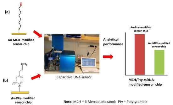
Evaluation of Polytyramine Film and 6-Mercaptohexanol Self-Assembled Monolayers as the Immobilization Layers for a Capacitive DNA Sensor Chip: A Comparison


Abstract
:
1. Introduction
2. Materials and Methods
2.1. Materials
2.2. Methods
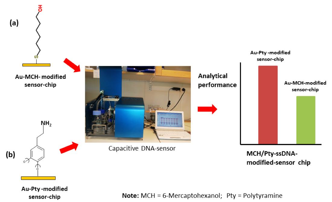
2.2.1. Cleaning and Modification of Sensor Chips
2.2.2. Immobilization of Capture Probe on the Modified Sensor Chips
2.2.3. Electrochemical Characterizations
2.2.4. Atomic Force Microscopy
- (i)
- Ra = average roughness
- (ii)
- Rz = ten-point mean height roughness
- (iii)
- Rq = root mean square roughness
- (iv)
- Rpv = peak to valley roughness
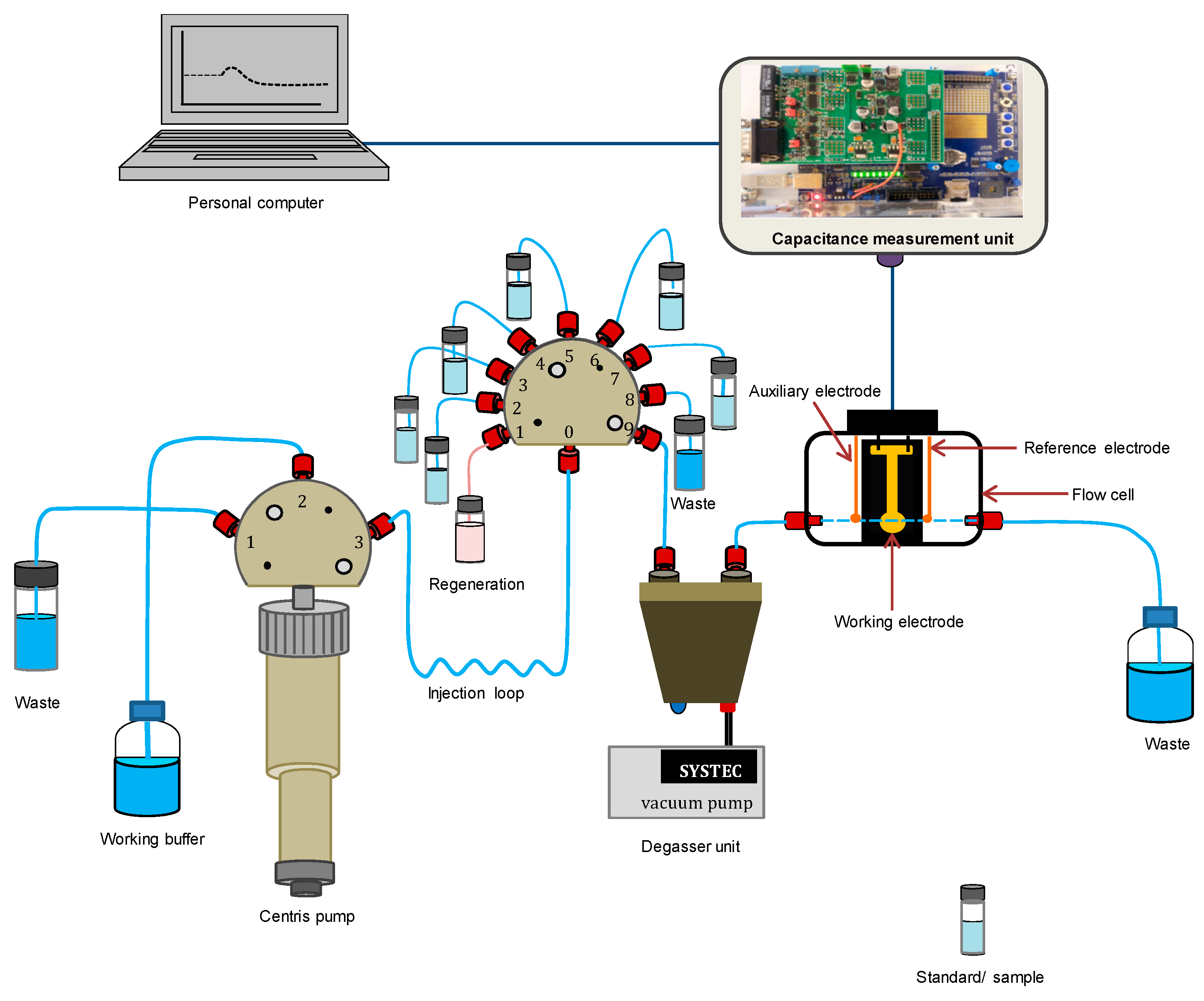
2.2.5. Capacitance Measurements
2.2.6. Analytical Characterizations
3. Results and Discussion
3.1. Optimum Deposition Conditions
3.2. Surface Coverage and Capacitance Baseline
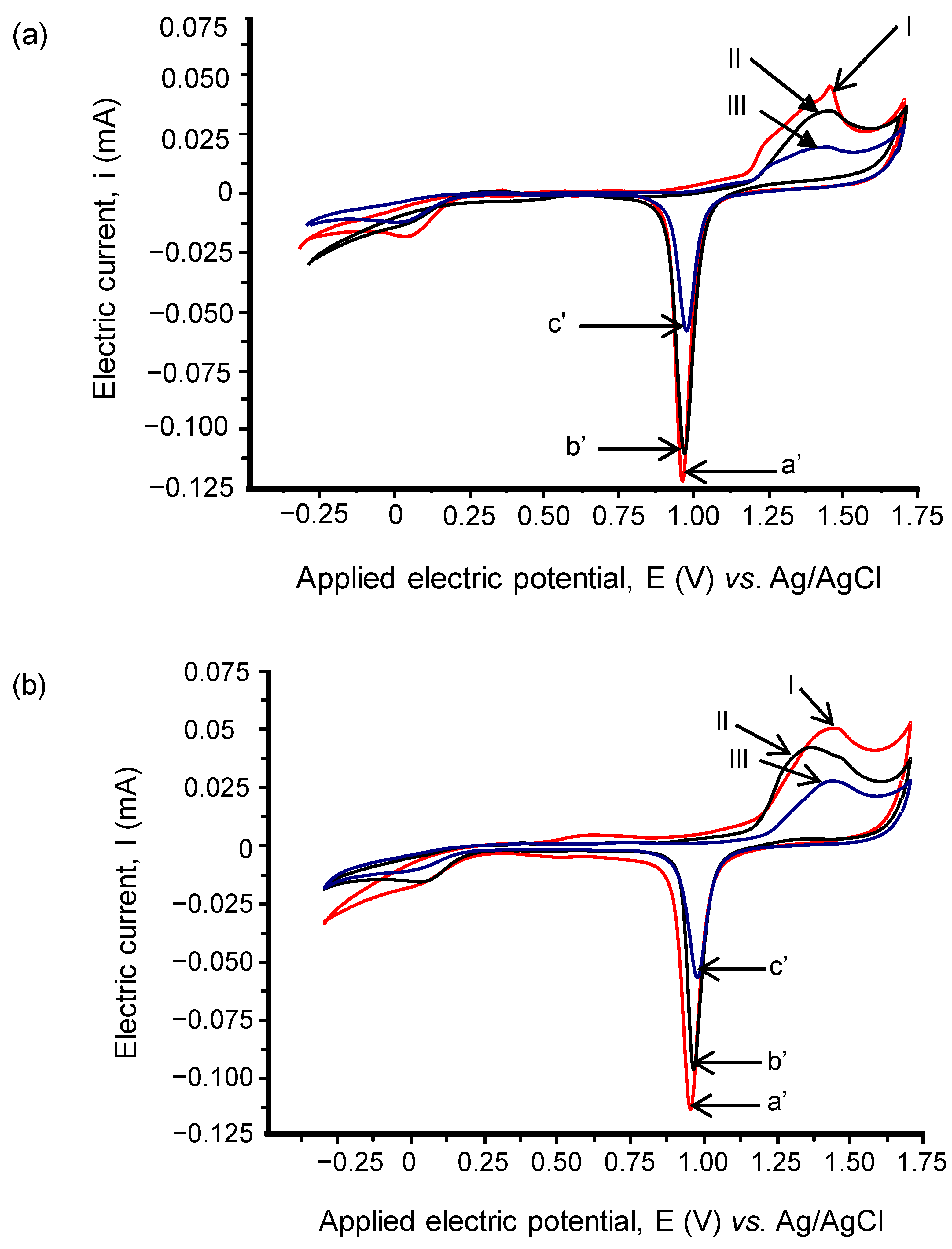
3.3. Electrochemical Properties
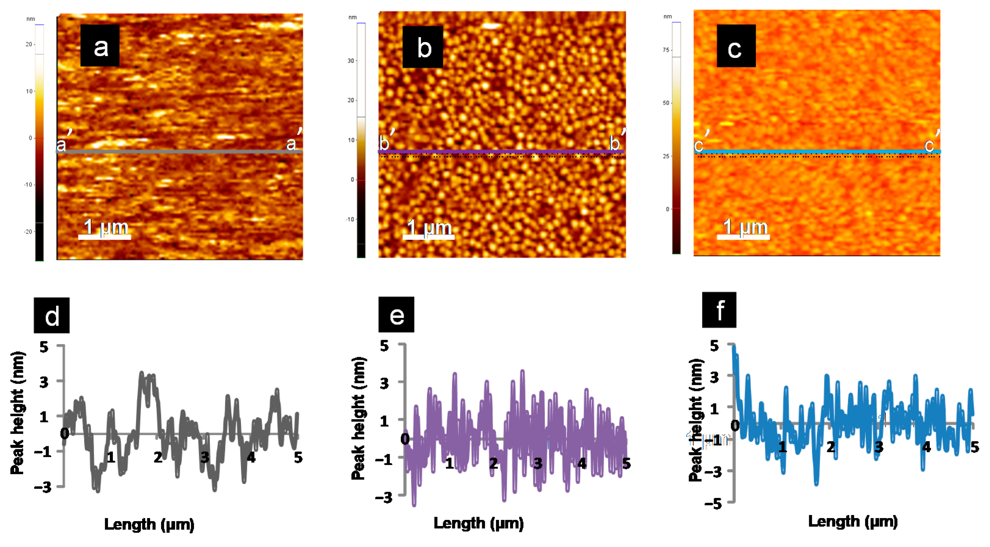
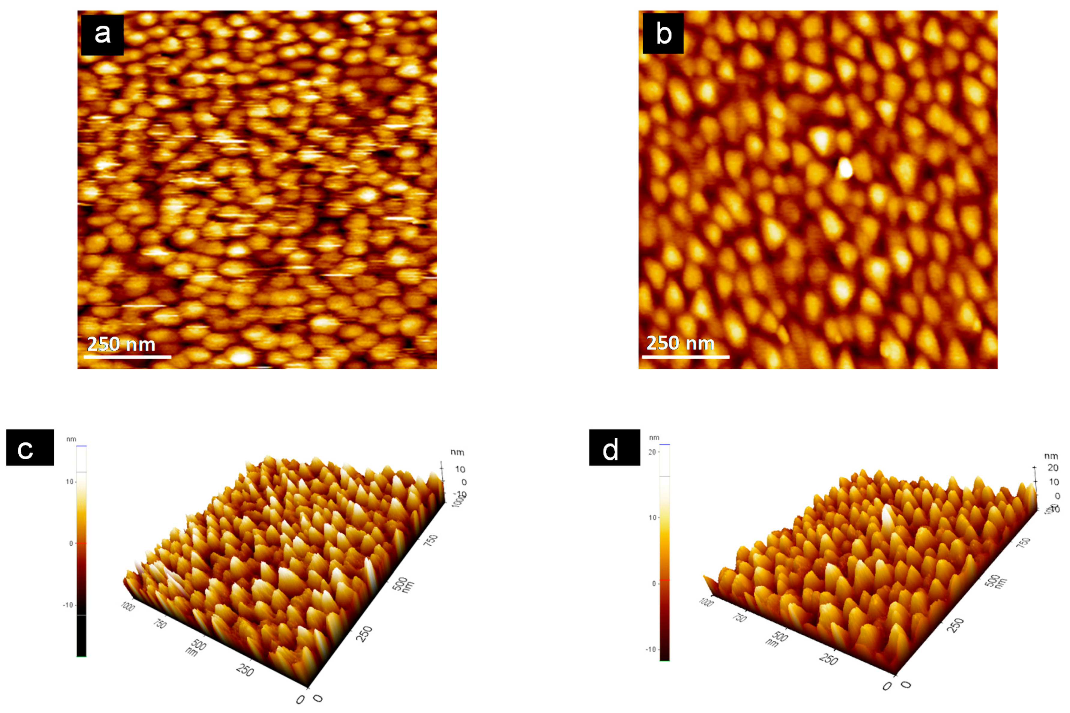
3.4. Topographical Analysis
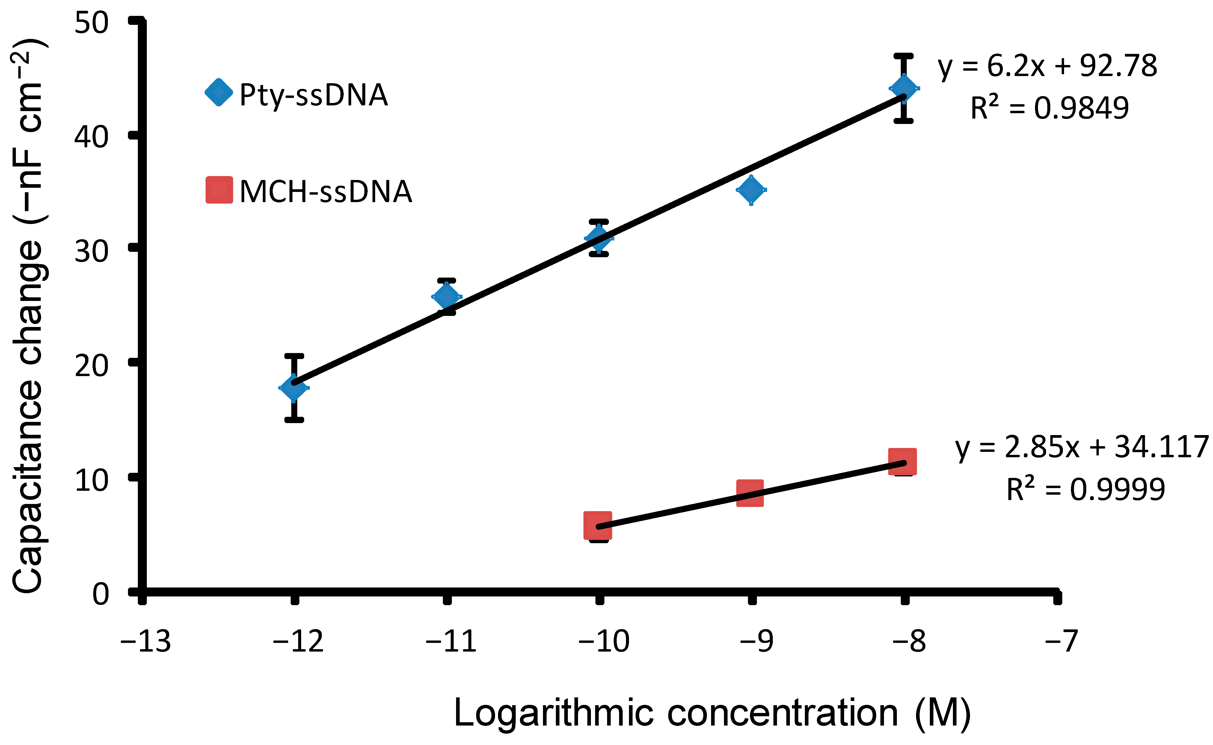
3.5. Sensitivity
3.6. Selectivity
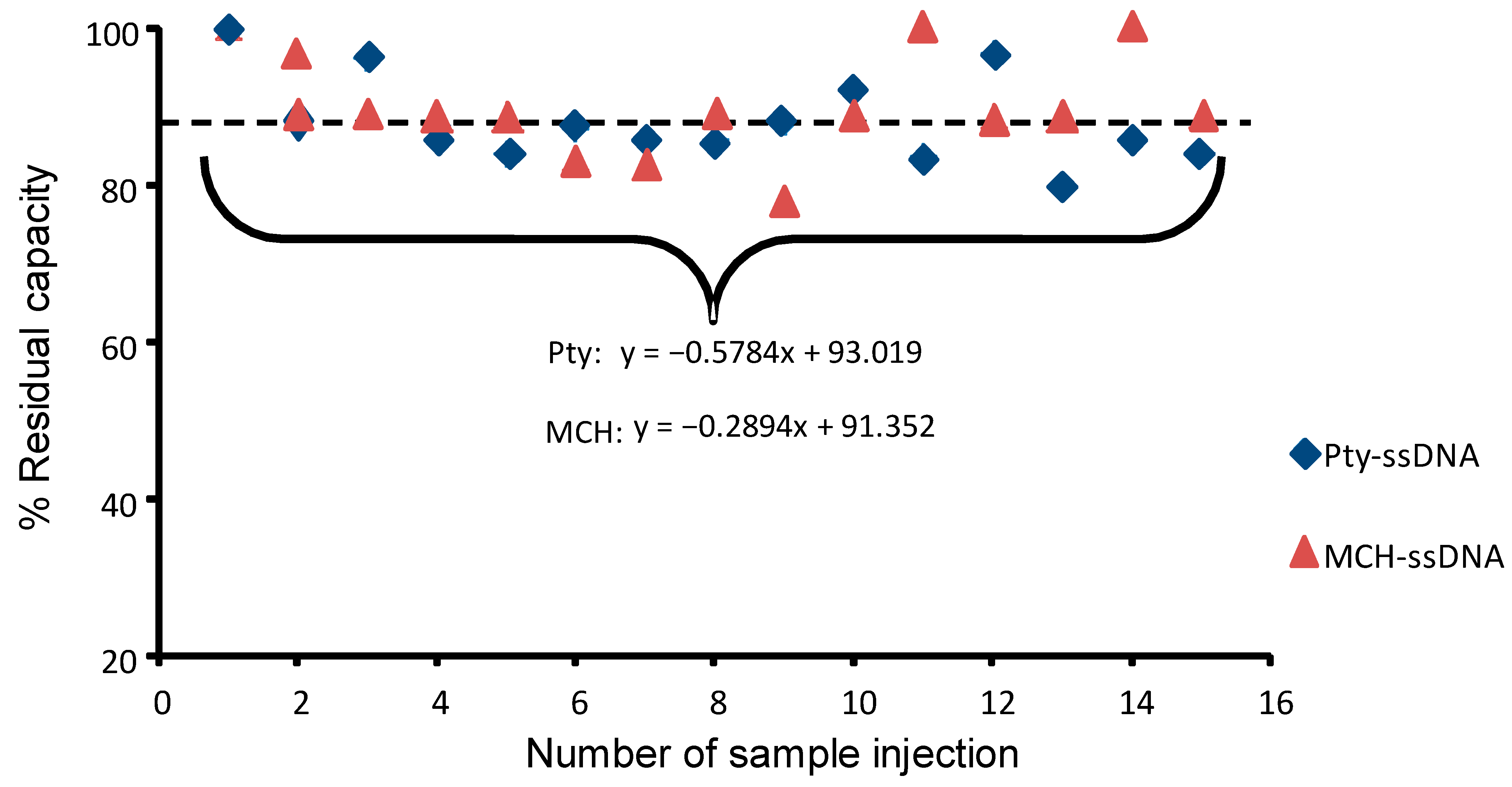
3.7. Re-Usability
4. Conclusions
Author Contributions
Funding
Institutional Review Board Statement
Informed Consent Statement
Data Availability Statement
Acknowledgments
Conflicts of Interest
References
- Ates, M. A review study of (bio) sensor systems based on conducting polymers. Mat. Sci. Eng. C Mater. 2013, 33, 1853–1859. [Google Scholar] [CrossRef]
- Malhotra, B.D.; Chaubey, A.; Singh, S.P. Prospects of conducting polymers in biosensors. Anal. Chim. Acta 2006, 578, 59–74. [Google Scholar] [CrossRef]
- Kros, A.; Sommerdijk, N.A.; Nolte, R.J.M. Poly(pyrrole) versus poly(3,4-ethylenedioxythiophene): Implications for biosensor applications. Sens. Actuators B Chem. 2005, 106, 289–295. [Google Scholar] [CrossRef]
- Peng, H.; Soeller, C.; Vigar, N.; Kilmartin, P.A.; Cannell, M.B.; Bowmaker, G.A.; Cooney, R.P. Label-free electrochemical DNA sensor based on functionalised conducting copolymer. J. Travas Sejdic. Biosens. Bioelectron. 2005, 20, 1821–1828. [Google Scholar] [CrossRef]
- Mahadhy, A.; Ståhl-Wernersson, E.; Mattiasson, B.; Hedström, M. Use of capacitive affinity biosensor for sensitive and selective detection and quantification of DNA—A model study. Biotechnol. Rep. 2014, 3, 42–48. [Google Scholar] [CrossRef] [Green Version]
- Mahadhy, A.; Mamo, G.; Ståhl-Wernersson, E.; Mattiasson, B.; Hedström, M. PRC-free ultrasensitive capacitive biosensor for selective detection and quantification of Enterobacteriacea DNA. J. Anal. Bioanal. Tech. 2014, 5, 210. [Google Scholar] [CrossRef] [Green Version]
- Lebogang, L.; Mattiasson, B.; Hedström, M. Capacitive sensing of microcystin variants of microcystis aeruginosa using a gold immunosensor-chip modified with antibodies, gold nanoparticles and polytyramine. Microchim. Acta 2014, 181, 9–10. [Google Scholar] [CrossRef]
- Sankoh, S.; Samanman, S.; Thipmanee, O.; Numnuam, A.; Limbut, W.; Kanatharana, P.; Vilaivan, T.; Thavarungkul, P. A comparative study of a label-free DNA capacitive sensor using a pyrrolidinyl peptide nucleic acid probes immobilized through polyphenylenediamine and polytyramine non-conducting polymers. Sens. Actuators B Chem. 2013, 177, 543–554. [Google Scholar] [CrossRef]
- Labib, M.; Hedström, M.; Amin, M.; Mattiasson, B. A novel competitive capacitive glucose biosensor based on concanavalin A-labeled nanogold colloids assembled on a polytyramine-modified gold electrode. Anal. Chim. Acta 2010, 659, 194–200. [Google Scholar] [CrossRef]
- Teeparuksapun, K.; Hedström, M.; Wong, E.Y.; Tang, S.; Hewlett, L.K.; Mattiasson, B. Ultrasensitive detection of HIV-1 p24 antigen using nanofunctionalized surfaces in a capacitive immunosensor. Anal. Chem. 2010, 82, 8406–8411. [Google Scholar] [CrossRef]
- Campuzano, S.; Pedrero, M.; Montemayor, C.; Fatas, E.; Pingarron, J.M. Characterization of alkanethiol-self-assembled monolayers-modified gold electrodes by electrochemical impedance spectroscopy. Electroanal. Chem. 2006, 586, 112–121. [Google Scholar] [CrossRef]
- Fu, Y.; Yuan, R.; Xu, L.; Chai, Y.; Zhong, X.; Tang, D. Indicator free DNA hybridization detection via EIS based on self-assembled gold nanoparticles and bilayer two-dimensional 3-mercaptopropyltrimethoxysilane onto a gold substrate. Biochem. Eng. 2005, 23, 37–44. [Google Scholar] [CrossRef]
- Piwonski, I.; Grobelny, J.; Cichomski, M.; Celichowski, G.; Rogowski, J. Investigation of 3-mercaptopropyltrimethoxysilane self-assembled monolayers on Au(III) surface. Appl. Surf. Sci. 2005, 242, 147–153. [Google Scholar] [CrossRef]
- Choi, J.W.; Park, K.S.; Lee, W.; Oh, B.K.; Chun, B.S.; Pae, S.H. Regulation of anti-LDL immobilization on self-assembled protein G layer using CHAPS and its application to immunosensor. Mat. Sci. Eng. C Mater. 2004, 24, 241–245. [Google Scholar] [CrossRef]
- Blasini, D.R.; Tremont, R.J.; Batina, N.; González, I.; Cabrera, C.R. Self-assembly of (3-mercaptopropyl) trimethoxysilane on iodine coated gold electrodes. Electroanal. Chem. 2003, 540, 45–52. [Google Scholar] [CrossRef]
- Park, S.; Weaver, M.J. A versatile surface modification scheme for attaching metal nanoparticles onto gold: Characterization by electrochemical infrared spectroscopy. J. Phys. Chem. B 2002, 106, 8667–8670. [Google Scholar] [CrossRef]
- Teeparuksapun, K.; Hedström, M.; Kanatharana, P.; Thavarungkul, P.; Mattiasson, B. Capacitive immunosensor for the detection of host cell proteins. Journal of Biotechnology. J. Biotechnol. 2012, 157, 207–213. [Google Scholar] [CrossRef] [PubMed]
- Labib, M.; Hedström, M.; Amin, M.; Mattiasson, B. A capacitive immunosensor for detection of cholera toxin. Anal. Chim. Acta 2009, 634, 255–261. [Google Scholar] [CrossRef]
- Zhao, Y.D.; Pang, D.W.; Hu, S.; Wang, Z.L.; Cheng, J.K.; Dai, H.P. DNA-modified electrodes; part 4: Optimization of covalent immobilization of DNA on self-assembled monolayers. Talanta 1999, 49, 751–756. [Google Scholar] [CrossRef]
- Limbut, W.; Kanatharana, P.; Mattiasson, B.; Asawatreratanakul, P.; Thavarungkul, P. A comparative study of capacitive immunosensors based on self-assembled monolayers formed from thiourea, thioctic acid, and 3-mercaptopropionic acid. Biosens. Bioelectron. 2006, 22, 33. [Google Scholar] [CrossRef]
- Berggren, C.; Bjarnason, B.; Johansson, G. Instrumentation for direct capacitive biosensors. Instrum. Sci. Technol. 1999, 27, 131–140. [Google Scholar] [CrossRef]
- Erlandsson, D.; Teeparuksapun, K.; Mattiasson, B.; Hedström, M. Automated flow-injection immunosensor based on current pulse capacitive measurements. Sens. Actuators B Chem. 2014, 190, 295–304. [Google Scholar] [CrossRef]
- Tichoniuk, M.; Ligaj, M.; Filipiak, M. Application of DNA hybridization biosensor as a screening method for the detection of genetically modified food components. Sensors 2008, 8, 2118–2135. [Google Scholar] [CrossRef] [PubMed] [Green Version]
- Sabatani, E.; Rubinstein, L.; Maoz, R.; Sagiv, J. Organized self-assembling monolayers on sensor-chips part I. Octadecyl derivatives on gold. Electroanal. Chem. 1987, 219, 365–367. [Google Scholar] [CrossRef]
- Raposo, M.; Ferreira, Q.; Ribeiro, P.A. A guide for atomic force microscopy analysis of soft-condensed matter. In Modern Research and Educational Topics in Microscopy; Méndez-Vilas, A., Díaz, J., Eds.; Formatex: Badajoz, Spain, 2007; Volume 1, pp. 758–769. [Google Scholar]
- Buck, R.P.; Lindner, E. Recommendations for nomenclature of ion-selective electrodes. Pure Appl. Chem. 1994, 66, 2527–2536. [Google Scholar] [CrossRef]
- Rivera-Gandia, J.; Cabrera, C.R. Self-assembled monolayers of 6-mercapto-1-hexanol and mercapto-n-hexyl-poly(dT)18-fluorescein on polycrystalline gold surfaces: An electrochemical impedance spectroscopy study. Electroanal. Chem. 2007, 605, 145–150. [Google Scholar] [CrossRef]
- Ladik, A.V.; Geiger, F.M.; Walter, S.R. Immobilization of DNA onto gold and dehybridization of surface-bound DNA on glass. Nanoscape 2001, 7, 19–23. [Google Scholar]
- Strike, D.J.; Derooij, N.F.; Koudelkahep, M. Electrochemical techniques for the modification of microelectrodes. Biosens. Bioelectron. 1995, 10, 61–66. [Google Scholar] [CrossRef]
- Losic, D.; Cole, M.; Thissen, H.; Voelcker, N.H. Ultrathin polytyramine films by electropolymerization on highly doped p-type silicon electrodes. J. Surf. Sci. 2005, 584, 245–257. [Google Scholar] [CrossRef]
- Vorburger, T.V. Methods for characterizing surface topography. In Tutorial in Optics; Moore, D.T., Ed.; Optical Society of America: Washington, DC, USA, 2010; pp. 137–151. [Google Scholar]
- Chaki, N.K.; Vijayamohanan, K. Self-assembled monolayers as a tunable platform for biosensor applications. Biosens. Bioelectron. 2002, 17, 1–12. [Google Scholar] [CrossRef]
- Tran, L.D.; Piro, B.; Pham, M.C.; Ledoan, T.; Angiari, C.; Dao, L.H.; Teston, F. A polytyramine film for covalent immobilization of oligonucleotides and hybridization. Synth. Met. 2003, 139, 251–262. [Google Scholar] [CrossRef]
- Sevenler, D.; Trueb, J.; Ünlüa, M.S. Beating the reaction limits of biosensor sensitivity with dynamic tracking of single binding events. Proc. Natl. Acad. Sci. USA 2019, 116, 4129–4134. [Google Scholar] [CrossRef] [Green Version]
- Yuqing, M.; Jianrong, C.; Xiaohua, W. Using electropolymerized non-conducting polymers to develop enzyme amperometric biosensors. Trends Biotechnol. 2004, 22, 227–231. [Google Scholar] [CrossRef] [PubMed]
- Zhou, L.; Shan, F.; Pravda, M.; Glennon, J.D.; Luong, J.H.T. Selective detection of dopamine using glassy carbon electrode modified by a combined electropolymerized permselective film of polytyramine and polypyrrole-1-propionic acid. Electroanalysis 2009, 21, 797–803. [Google Scholar] [CrossRef] [Green Version]
- Mahadhy, A.; Ståhl-Wernersson, E.; Mattiasson, B.; Hedström, M. Rapid detection of mecA gene of methicillin-resistant Staphylococcus aureus by a novel, label-free real-time capacitive biosensor. Biotechnol. Rep. 2020, 28, 1–5. [Google Scholar] [CrossRef] [PubMed]


| Parameter(s) | Bare Sensor Chip | Pty-Only Sensor Chip | MCH-Only Sensor Chip | Pty-ssDNA Sensor Chip | MCH-ssDNA Sensor Chip |
|---|---|---|---|---|---|
| % surface coverage | 0 | 65 ± 2 | 26 ± 2 | 75 ± 3 | 30 ± 2 |
| Capacitance/baseline (nF cm−2) | 10,420 | 10,790 | 8510 | 11,040 | 9140 |
| Surface | Ra (nm) | Rz (nm) | Rq (nm) | Rpv (nm) |
|---|---|---|---|---|
| Bare | 2.90 | 14.50 | 3.35 | 16.00 |
| Pty | 3.60 | 20.40 | 4.60 | 25.10 |
| MCH | 3.10 | 17.50 | 3.85 | 21.70 |
| Pty-ssDNA | 3.80 | 14.00 | 4.60 | 18.30 |
| MCH-ssDNA | 2.50 | 11.30 | 3.20 | 15.70 |
Publisher’s Note: MDPI stays neutral with regard to jurisdictional claims in published maps and institutional affiliations. |
© 2021 by the authors. Licensee MDPI, Basel, Switzerland. This article is an open access article distributed under the terms and conditions of the Creative Commons Attribution (CC BY) license (https://creativecommons.org/licenses/by/4.0/).
Share and Cite
Mahadhy, A.; Mattiasson, B.; StåhlWernersson, E.; Hedström, M. Evaluation of Polytyramine Film and 6-Mercaptohexanol Self-Assembled Monolayers as the Immobilization Layers for a Capacitive DNA Sensor Chip: A Comparison. Sensors 2021, 21, 8149. https://doi.org/10.3390/s21238149
Mahadhy A, Mattiasson B, StåhlWernersson E, Hedström M. Evaluation of Polytyramine Film and 6-Mercaptohexanol Self-Assembled Monolayers as the Immobilization Layers for a Capacitive DNA Sensor Chip: A Comparison. Sensors. 2021; 21(23):8149. https://doi.org/10.3390/s21238149
Chicago/Turabian StyleMahadhy, Ally, Bo Mattiasson, Eva StåhlWernersson, and Martin Hedström. 2021. "Evaluation of Polytyramine Film and 6-Mercaptohexanol Self-Assembled Monolayers as the Immobilization Layers for a Capacitive DNA Sensor Chip: A Comparison" Sensors 21, no. 23: 8149. https://doi.org/10.3390/s21238149
APA StyleMahadhy, A., Mattiasson, B., StåhlWernersson, E., & Hedström, M. (2021). Evaluation of Polytyramine Film and 6-Mercaptohexanol Self-Assembled Monolayers as the Immobilization Layers for a Capacitive DNA Sensor Chip: A Comparison. Sensors, 21(23), 8149. https://doi.org/10.3390/s21238149