Article

The Role of Noise in Specific Detectivity of InAs/GaSb Superlattice MWIR Bariodes

1
Łukasiewicz Research Network—Institute of Microelectronics and Photonics, al. Lotników 32/46, 02-668 Warsaw, Poland
2
Department of Electronics Fundamentals, Rzeszow University of Technology, W. Pola 2, 35-959 Rzeszow, Poland
*
Author to whom correspondence should be addressed.
Sensors 2021, 21(21), 7005; https://doi.org/10.3390/s21217005
Submission received: 2 October 2021 / Revised: 17 October 2021 / Accepted: 19 October 2021 / Published: 22 October 2021
(This article belongs to the Section Electronic Sensors)

Abstract

:
In this paper, the results of the electrical, noise, and optical characterization of p-i-n and p-B-i-n diodes with AlSb and 4 ML AlSb/8 ML GaSb superlattice barriers in High-Operating Temperature conditions, are presented. Experimental and theoretical noise parameters were compared. Both dark current and noise analysis showed that the p-Bp_bulk-i-n bariode had the best performance. P-i-n photodiodes had the highest experimental value of specific detectivity (D*) of 6.16 × 10⁹ Jones at 210 K and zero bias. At about −1 V reverse bias, the bariode with AlSb/GaSb electron barrier caught up to it and both devices achieved D* = (1–1.1) × 108 Jones. Further optimization of the superlattice-based electron barrier should result in the improvement of bariode performance at a smaller bias, at which better noise performance is more pronounced. It was shown that neglecting the low-frequency noise component can lead to a significant overestimation of detectivity. The simple method of incorporation of low-frequency noise contribution in the detectivity calculation, without time-consuming measurements, has been proposed.

1. Introduction

Infrared photodetectors are widely used in many branches of modern society such as environment monitoring, imaging, medicine, spectroscopy, or the military. Presently, mercury-cadmium-telluride-based technology dominates the market. However, national and international legislation works to eliminate heavy metal usage in the production of consumer products, including Hg and Cd. As a result, research to find better and safer materials is undergoing in facilities around the world. At present, two of the best candidates are antimonide-based type-II superlattices (SL) InAs/GaSb and InAs/InAsSb [1,2,3,4,5]. They allow for the utilization of bandgap engineering design structures with long-wavelength absorption edge practically in the entire mid-infrared spectral range [6]. Furthermore, both their growth and processing technology matured in the last decade to the point, at which discrete photodetectors, as well as focal plane arrays based on them, are becoming more common [7,8,9].
Lately, more and more attention is paid to the High-Operating Temperature (HOT) photodetectors, which work at temperatures from 200 K to 300 K and beyond [10,11,12]. In such devices, low temperatures are achieved through the use of thermoelectric cooling. They have many advantages over cryogenically cooled detectors. In particular, they allow for further decreasing the size and weight, lowering production costs as well as better power usage efficiency. As a result, their applications can be more versatile and more easily spread into the consumer market.
Increasing the operating temperature of SL-based infrared photodetectors can be achieved using different approaches. One is to use novel architecture, such as in Interband Cascade Detectors or Quantum Cascade Detectors [13,14]. Presently, the main disadvantage of such structures is their complexity. They require considerable computational effort during the design and optimization stages. Furthermore, they are hard to realize epitaxially, as the margin of error required for their proper operation is very small. Another approach is to introduce unipolar carrier barriers into mature detector designs (e.g., photoconductor or p-i-n photodiode), the purpose of which is the suppression of dark current and noise without negatively influencing the photocurrent [15,16,17]. The barriers can be placed for one or two types of carriers, depending on the detector structure. They can be made of either bulk material (e.g., AlSb, AlAsSb, AlGaSb) or superlattice (e.g., InAs/AlSb, AlSb/GaSb). The latter allows for better optimization of the photodetector band structure due to the utilization of bandgap engineering.
This paper is focused on photodiodes with (p-Bp-i-n) and without (p-i-n) electron barriers, based on a double heterojunction design. The Bp in p-Bp-i-n pertains to a p-type electron barrier made of either AlSb or AlSb/GaSb superlattice. The analysis of dark current, noise, and optical response is presented. The emphasis was put on the role of noise in the performance of these infrared photodetectors. Furthermore, a comparison between two semi-empirical approximations (the first including thermal and shot noise, and the second including thermal, shot, and low-frequency noise) and actual measurements is presented. The issues arising from the omission of low-frequency noise during the calculation of specific detectivity and resulting errors are addressed. Usually, noise figures for InAs/GaSb-superlattice-based devices are given for low temperatures <150 K, which is understandable since cryogenically-cooled detectors are most commonly used [18,19,20]. In this paper, all noise characteristics are shown in the HOT temperature range in addition to the low-temperature characterization. Furthermore, to the best of our knowledge, there are no low-frequency noise measurements reported for bariodes on GaAs substrate, in contrast to recently reported results for various detectors on GaSb substrate [19,21,22].

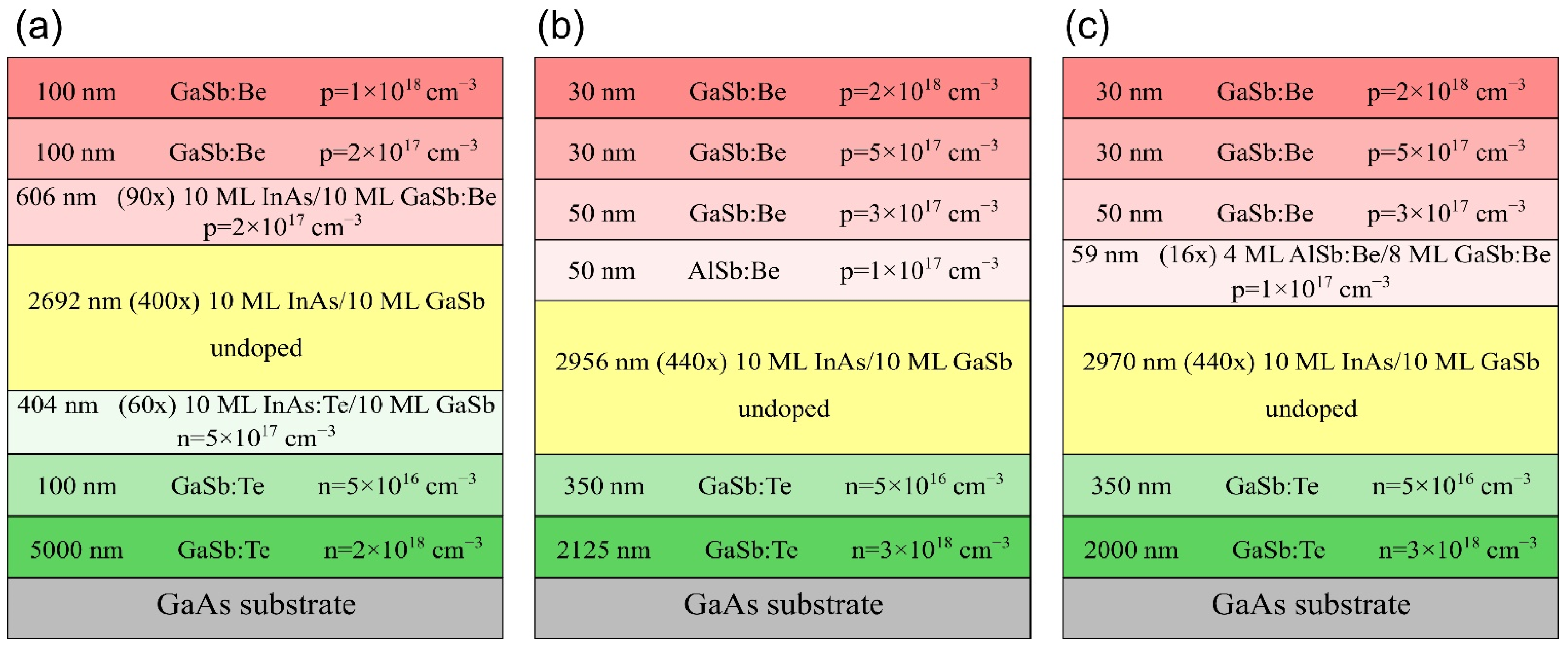
2. Fabrication of InAs/GaSb Superlattice Photodetectors

In this work, three types of photodiodes were compared, namely p-i-n, p-Bp_bulk-i-n with AlSb electron barrier, and p-Bp_SL-i-n with type-I AlSb/GaSb superlattice electron barrier. In Figure 1, schematic diagrams of each photodetector are shown. All samples were deposited on (100) GaAs substrates.
Photodetector heterostructures were grown using molecular beam epitaxy in Riber 32P reactor. In both types of structures, p-type and n-type contact layers were made of highly doped (~1018 cm−3) GaSb material. The absorption region consisted of 400 to 440 periods of type-II 10 ML InAs/10 ML GaSb superlattice with InSb-like and GaAs-like interfaces. The epitaxial growth of the superlattice was described elsewhere [23]. Before fabrication of p-Bp_SL-i-n photodiodes, the growth of 4 ML AlSb/8 ML GaSb superlattice was optimized. A series of test processes were performed, which culminated in high-quality material. In Figure 2a, the 2θ/ω curve measured for AlSb/GaSb superlattice using the high-resolution x-ray diffraction (HRXRD) method is shown. From its analysis, the following information was obtained: AlSb layer thickness—4.1 ML (12.5 Å; ML stands for monolayer), GaSb layer thickness—8.3 ML (25.3 Å), and perpendicular lattice mismatch (Δa/a) of 4240 ppm. The latter is defined as follows:
( Δ a / a ) = a _ SL 0   a _ GaSb a _ GaSb ,
where a⊥_SL0 is the perpendicular lattice constant of the superlattice, for which lattice mismatch is calculated, and a⊥_GaSb is the perpendicular lattice constant for GaSb substrate (for test AlSb/GaSb superlattice) or GaSb buffer layer (for photodiode/bariode structures). The zeroth-order satellite peak has an FWHM of 144 arcsec. The presence of Pendellösung peaks confirmed parallelism of crystallographic planes. Furthermore, this AlSb/GaSb superlattice exhibited a smaller lattice-mismatch to the GaSb than bulk AlSb.
Device heterostructures underwent structural quality tests using the HRXRD method. In Figure 2b–d, 2θ/ω curves are shown. The summary of structural details of photodiode heterostructures under consideration and lattice mismatch (Δa/a) between both absorber superlattices and barriers and GaSb buffer are given in Table 1. For all samples, higher-order satellite peaks up to the fifth order are observable, which is an indication of their high quality. The AlSb/GaSb superlattice electron barrier in p-Bp_SL-i-n heterostructure differed slightly from the test one. The layer thicknesses were AlSb—4.4 ML, GaSb—7.6 ML, and (Δa/a) was 4950 ppm.
Photodetectors were designed to operate in back-side illumination configuration and p-type contact layers are on the top of the structure. There were three reasons behind this choice. Firstly, it was to minimize losses related to the high free-carrier absorption in p-type GaSb in the mid-wavelength spectral range. Secondly, materials used as electron barriers have a large value of (Δa/a) to the buffer, namely 11,800 ppm for AlSb and 4950 ppm for 4 ML AlSb/8 ML GaSb. It could result in worsening of both structural and optical quality of 10 ML InAs/10 ML GaSb absorber superlattice if grown on top of such barrier layers. It would also negatively impact figures of merit of the photodetector. Finally, a double pass of infrared light through the absorption region could be achieved in such a configuration due to reflection from the top contact. Barriers were intentionally doped with beryllium to minimize the effects of valence band offsets between them and neighboring layers.
After the growth, heterostructures were further processed. Circular mesa structures were formed using the reactive ion etching-inductively coupled plasma dry etching method. The diameters of the photodiodes were 300 μm. Electrical contacts were made by the deposition of Ti/Au metallization using the magnetron sputtering method. After dicing, sample photodetectors were mounted onto test sub-assemblies using wire bonding. Finally, dark current, noise, and optical characterizations were performed.

3. Results and Discussion

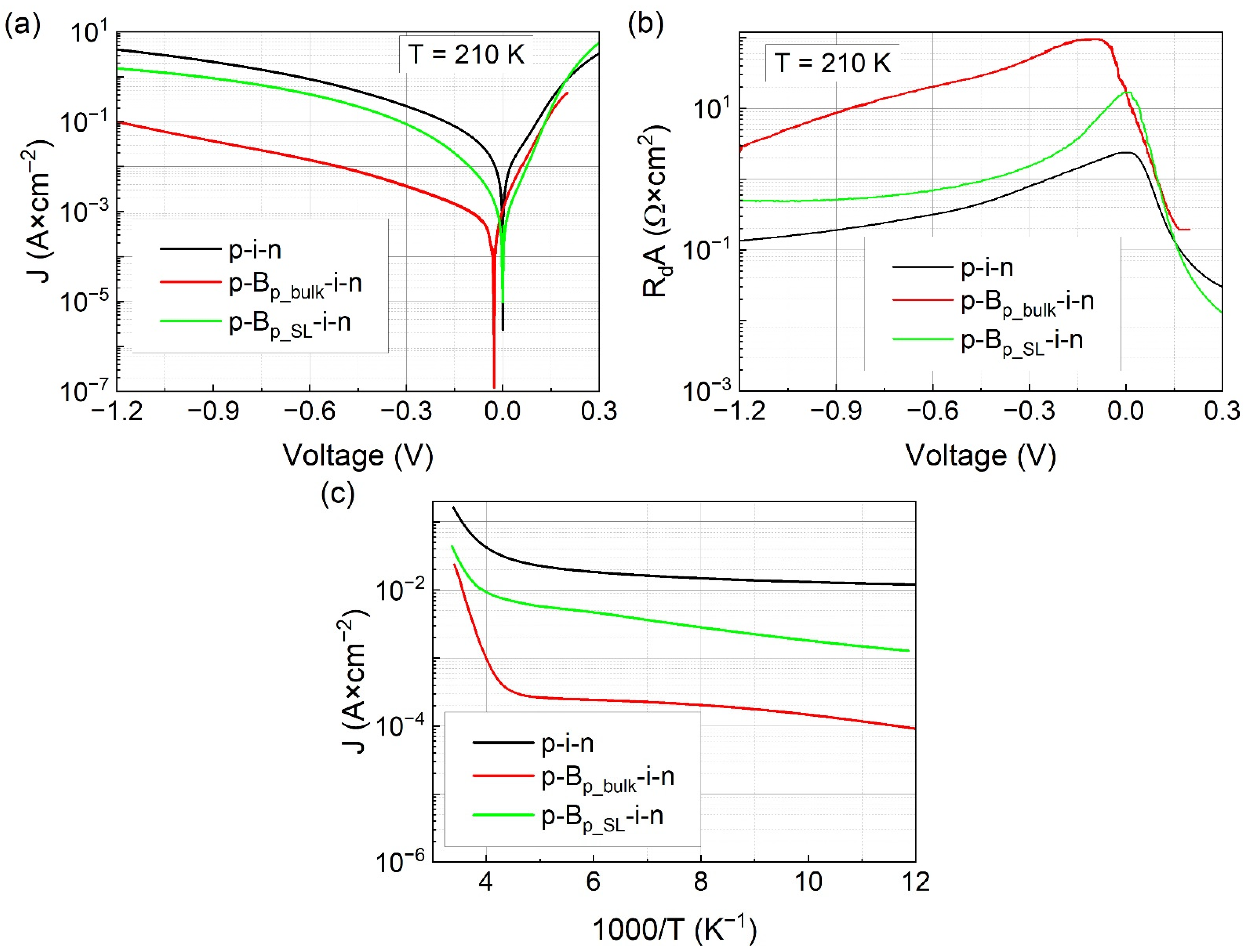
3.1. Dark Current Characteristics

Dark current-voltage characteristics were measured for each photodiode in a wide range of temperatures using a setup consisting of Keithley 2612A source-measure instrument and Janis CCS-150 closed-cycle cryocooler. Samples were isolated from the environmental background radiation using a cold shield, which was cooled to around 10 K during the measurements. Differential-resistance-area product (RdA) as a function of bias was calculated from experimental I–V data. In Figure 3a,b, J–V and RdA–V curves for considered photodiodes at 210 K are shown, respectively. This temperature was chosen as it corresponds to the one achievable through miniature three-stage thermoelectric coolers. Large differences in electrical characteristics between particular photodetectors were observed. The lowest dark current density was obtained for the p-Bp_bulk-i-n bariode, whereas the highest was for the p-i-n diode. Comparison between bariodes indicated that p-Bp_SL-i-n has a higher dark current. Both unbiased barrier photodiodes had similar values of R0A parameter of about 17 Ωcm2 for p-Bp_bulk-i-n and ~18 Ωcm2 for p-Bp_SL-i-n. However, for the latter device, it was the highest value whereas p-Bp_bulk-i-n achieved a higher value of ~100 Ωcm2 with a small reverse bias of 104 mV. The classic p-i-n photodiode had a maximum RdA value of 2.4 Ωcm2 for zero bias. It is noteworthy that the photodetectors in this paper were not passivated, which could further decrease the dark current density.
In Figure 3c, dark current densities at −50 mV bias are plotted as a function of reciprocal temperature. The p-i-n photodiode had the highest dark current density in the entire temperature range of 77 K–300 K. The p-Bp_bulk-i-n bariode had the smallest dark current density and outperformed the p-Bp_SL-i-n by more than one order of magnitude for T < 200 K. In Table 2, activation energies Ea2 and Ea3 obtained from the analysis of the curves in Figure 3c and their corresponding temperature ranges are given. All photodiodes had very small (<10 meV) activation energies in low-temperature ranges (ΔT2 and ΔT3), which suggests surface leakage channel as the main shunt current source. A more detailed analysis is needed to identify a specific mechanism. The behavior of photodiodes differs more at higher temperatures (ΔT1). The activation energies Ea1 for the p-Bp_SL-i-n bariode and the p-i-n photodiode were close to half of their bandgap energy at 300 K (Eg_300 K), which were equal to ≈250 meV and 235 meV, respectively. These values indicate that the operation of these detectors in the ΔT1 temperature range is limited by the generation-recombination (g-r) component of the dark current and/or shunt currents since it was shown that they can exhibit similar behavior and are influenced by the defect states in the junction area [24]. On the other hand, p-Bp_bulk-i-n had the highest activation energy, which was closer to the value of Eg_300 K ≈ 250 meV (Ea1 ≈ 0.88 × Eg_300 K). This suggests that both diffusion and g-r dark current components are limiting its performance, with the former being the dominant one. The values of Eg_300 K for p-i-n photodiode were estimated using the Varshni relation, which is described in Section 3.3. On the other hand, the Eg_300 K for both bariodes was determined from measurements of spectral current responsivity RI at 300 K (not shown in the paper).

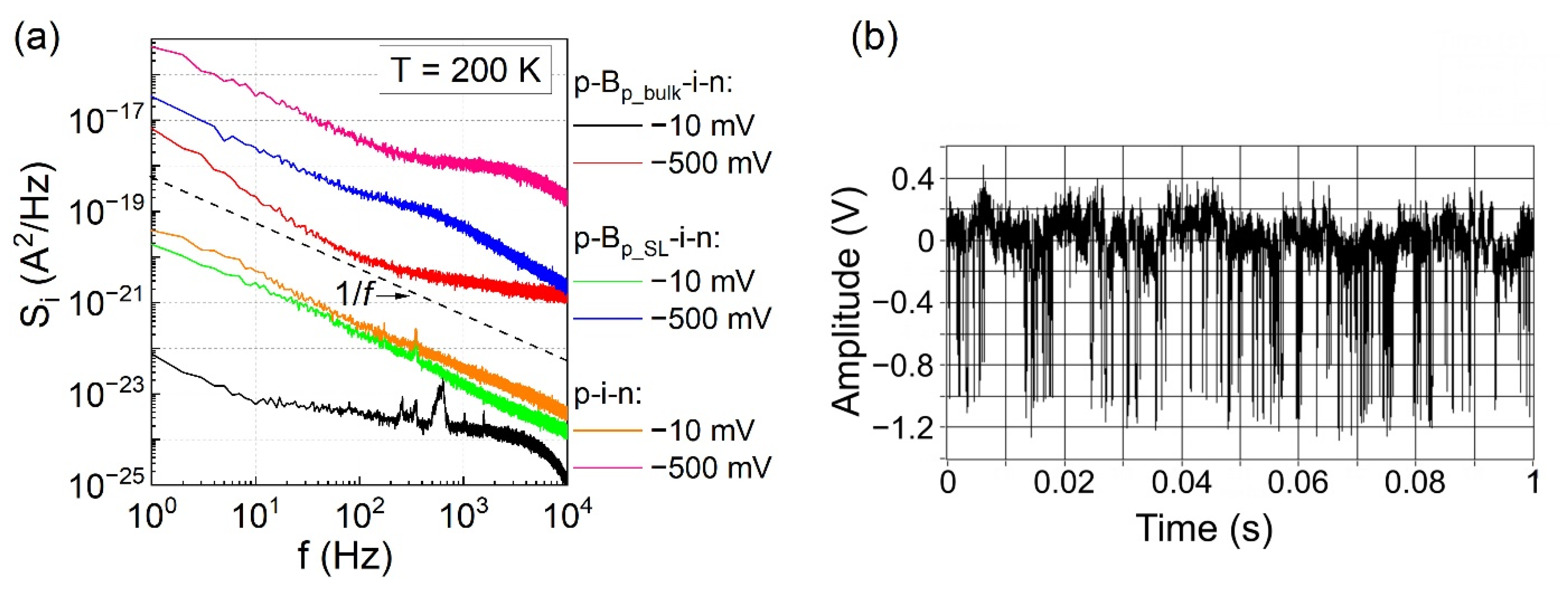
3.2. Noise Characteristics

The setup used for low-frequency noise measurements and the small-signal equivalent circuit of a photodiode were described in Ref. [25]. In Figure 4a, power spectral densities measured at T = 200 K for the low and high bias voltages are shown. In general, power spectral densities exhibit 1/f dependence, but some Lorentzian (Si ~1/(1 + (f/const.)2) inclusions appear, especially for the low biased detector with a bulk AlSb barrier. The analysis of the noise signal in the time domain, illustrated in Figure 4b, reveals that Lorentzian is connected with random telegraph noise (RTN). Such noise is attributed to the carrier capture/emission by extended defects present in the depletion region [26]. At a small voltage bias of −10 mV, the low-frequency noise magnitude is the lowest for the p-Bp_bulk-i-n detector. The significant difference in the magnitude is especially observed for low bias voltage and at low frequencies. For U = −500 mV, p-i-n photodiode had the highest noise magnitude in the entire measured frequency range, whereas p-Bp_bulk-i-n had the smallest. The p-Bp_SL-i-n was in-between, however, its Si decreased to the level of p-Bp_bulk-i-n at f ≈ 10 kHz.
In Figure 5a,b, power spectral density magnitude Si(f = 1 Hz) measured at T = 84 K and T = 200 K are shown as a function of bias current I. The dashed line in this figure follows dependence Si(f = 1 Hz) ~I2. The measured characteristics Si(I) match Si(I) ~I2 dependence closely. There is no significant difference in the Si(I) magnitude for three considered types of photodetectors. If squared, dependence between Si(I) and I holds, the noise coefficient can be defined as α = Si(f = 1 Hz)/I2. The noise coefficients as a function of temperature are shown in Figure 5b. In this experiment, the noise was measured at voltage bias U = −50 mV. In the low-temperature region (T ≈ 84 K), the noise coefficient for all three structures is within the range of 1 × 10⁻⁹–2 × 10⁻⁸ Hz−1. The current-temperature characteristics (see Figure 3c) show that in the low-temperature region, the leakage shunt current Ish dominates. Different values of noise coefficient αsh = Si(f = 1 Hz)/(Ish)2, related to the shunt current, have been reported in the literature. For InAs/GaSb SL devices, αsh is within the range of 3 × 10⁻¹⁰–6 × 10⁻⁶ Hz−1 [21,27]. Our values of αsh lie in the middle of that range and change with the temperature only slightly. In the high-temperature region, the diffusion and generation-recombination currents dominate the total current. It was shown that such current, especially the diffusion component, has a much lower noise coefficient [18,21,27,28,29]. For detectors with InAs/GaSb SL absorber, αg-r = 4.8 × 10⁻⁹ Hz−1 and αdiff = 1.9 × 10⁻¹⁰ Hz−1 were found for generation-recombination and diffusion current, respectively [19]. In the high-temperature region, the noise coefficient decreases slightly for p-i-n, p-Bp_SL-i-n because the shunt current is still significant for these structures as compared to the diffusion current. For p-Bp_bulk-i-n, with low shunt current, the noise coefficient drops suggestively reaching a value of 1 × 10⁻¹¹ Hz−1, which is much lower than the best (lowest) results found by us in the literature [19]. This translates into good noise performance of the p-Bp_bulk-i-n detector at temperatures, where current is limited by its diffusion component.

3.3. Optical Characteristics

Spectral current responsivity measurements were performed in the range of 3–6 μm at 210 K. The experimental setup consisted of Horiba MicroHR motorized monochromator equipped with SiC-based IR source and ruled grating with blaze wavelength of 5000 nm. The optical signal was mechanically chopped and detected using the Stanford Research Systems SR830 DSP lock-in amplifier. A calibrated lithium tantalate pyroelectric detector with a BaF2 window was used to measure the reference signal. Sample photodetectors were placed in Janis CCS-150K closed-cycle cryocooler with a KBr window.
In Figure 6a–c, results of spectral current responsivity (RI) measurements of considered photodetectors are shown for two reverse bias values each. Long-wavelength absorption edge λc was determined to be ~4.7 μm for all analyzed photodiodes. The cause of the slight differences in λc originates mainly from the variations in both the composition and thicknesses of InSb- and GaAs-like interfaces in the InAs/GaSb superlattice in the absorption region. The former were not taken into account during the simulation of 2θ/ω curves, in which binary interfaces were assumed. The latter are given in Table 1 in the section Fabrication of InAs/GaSb superlattice photodetectors. Dips in the spectra at wavelengths in the range of 3.3–3.5 μm in Figure 6a–c are caused by the absorption of radiation by water vapor present in the measurement chamber.
In Figure 6d, experimental values of bandgap energy Eg determined from RI measurements at various temperatures for p-i-n photodiode are plotted. The data were fitted to Varshni relation (red line in Figure 6d), and the following parameters were obtained: Eg_0 = 300 meV, α = 4.09 × 10⁻⁴ eV × K−1. The β = 270 K was assumed as it is most commonly used for InAs/GaSb type-II superlattices [30,31]. The fitting was performed for p-i-n photodiode only. For bariodes, RI spectra were measured only at 2–3 different temperatures. The values of Eg of absorber region in p-i-n, p-Bp_bulk-i-n, and p-Bp_SL-i-n photodiodes at 210 K were 263 meV, 271 meV, and 273 meV, respectively. As was mentioned, the difference in Eg results from variation in thickness of InSb-like and GaAs-like interfaces in InAs/GaSb superlattice (Table 1).
The measured spectral current responsivity of p-i-n photodiode increased with reverse bias from ~1.2 A × W−1 for U = 0 V to ~1.65 A × W−1 for U = −0.9 V. It also had the highest values of RI, namely ~1.65–1.68 A × W−1 for wavelengths in the range from 3.55 μm to 4 μm. The photodiode with the AlSb barrier had the lowest RI, which was less than 0.04 A × W−1 in the entire measurement range. Two reverse biases were considered at 0 V and about −1 V. The presence of p-n junction in all described heterostructures should enable a passive operation of these photodetectors without bias. This is clear for the p-i-n diode, for which spectral current responsivity is nearly the same with and without bias. In principle, the addition of a barrier for electrons should not negatively impact carrier transport in the heterostructure and thus device operation. This is under the condition that the barrier layer will not introduce parasitic valence band offset between absorption and/or contact regions. Based on the curves shown in Figure 6b,c for U = 0 V, it is clear that an unwanted barrier for holes in the valence band is present. Both for p-Bp_bulk-i-n and p-Bp_SL-i-n bariodes, RI was less than 5 mA × W−1. To overcome the potential barrier, an external bias was necessary.
Spectral current responsivity was measured for various biases from 0 V to 1 V. The values of the voltage result from the limitations of the measurement setup at the time. In the case of the p-i-n photodiode, the responsivity did not change with increasing voltage. For bariodes, both p-Bp_bulk-i-n and p-Bp_SL-i-n, RI increased with reverse bias. Despite the improvement, the RI for the photodetector with the AlSb barrier was very small, <40 mA × W−1. This indicates that the applied external electric field failed to completely overcome the parasitic barrier in the valence band and improve device operation. On the other hand, p-Bp_SL-i-n bariode reached maximum RI = 1.33 A × W−1, which corresponds to about 260 times improvement. This proves that AlSb/GaSb superlattice plays a much better role as an electron barrier than the bulk AlSb layer. Nevertheless, further optimization of the AlSb/GaSb structure is necessary to eliminate the parasitic valence band offset and improve device performance.

3.4. Specific Detectivity

Finally, the values of specific detectivity D* based on two semi-empirical approximations (D*approx._1, D*approx._2) and measured (D*exp) Si were determined and juxtaposed. The calculations were performed for two bias voltages (0 V and ~−1 V), for λ = 4 μm, T = 210 K, and f = 10 kHz. In general, the D* for a bandwidth of 1 Hz can be defined as follows:
D   = R I A S i ,
where RI is the spectral current responsivity, A is the area of the detector, and Si is the noise power spectral density at a given frequency. The Si can be further described as:
S i =   S i _ thermal +   S i _ Schottky +   S i _ lf + S i _ other = 4 k B T R + 2 qI +   α I b f + S i _ other ,
where Si_thermal is thermal noise PSD, Si_Schottky is shot noise PSD, Si_lf is low-frequency noise PSD, Si_other is the sum of other (not included) noise power spectral densities, kB is Boltzmann’s constant, T is temperature, R is dynamic resistance, q is the elementary charge, I is current, b is the power coefficient, which is usually assumed equal to 2, α is the noise coefficient, and f is frequency. In our case, the Slf can be expressed as in Equation (3), assuming α = 2, due to the behavior of the data shown in Figure 5a. To most accurately determine the specific detectivity it is necessary to measure the noise PSD for a specific device. However, when this is not an option, it is possible to use semi-empirical approximations of Si. The first approximation (Si_approx._1) includes only thermal and shot noise components. It is calculated using I and R extracted from the measured current-voltage curves of a photodetector. The second approximation (Si_approx._2) includes thermal, shot, and low-frequency noise components. On top of I and R, it requires information about the noise coefficient α. In this approach, it is sufficient to measure α for a specific bias (not necessarily the voltage for which the detectivity will be determined), for example, −50 mV in this paper as shown in Figure 5c. Then, Si_lf can be estimated using the expression given in Equation (3) for voltage bias, for which the Si(I) ~I2. Both approximations can be further simplified, depending on the bias of the photodiode. For unbiased photodetectors, in the absence of photocurrent due to background radiation, the specific detectivity will be limited only by thermal noise. The accuracy of these approximations depends on the interaction between the aforementioned noise components, which is related to the type of the photodetector, the quality of its structure, and processing. Furthermore, their usage may lead to both under- and overestimation of D*, especially under improper assumptions.
The first approximation (Si_approx._1) was used to estimate the specific detectivity D*approx._1 for unbiased and biased photodiodes in question. For U = 0 V the Si_Schottky was about four, two, and one order of magnitude smaller than Si_thermnal for p-i-n, p-Bp_bulk-i-n, and p-Bp_SL-i-n, respectively. The non-zero shot noise component originates from the photocurrent generated due to the background radiation. The following voltages, which were used during spectral current responsivity measurements, were used in the calculation of D* under bias: −0.9 V for p-i-n, −1 V for p-Bp_bulk-i-n, and −1.12 V for p-Bp_SL-i-n. In this case, the average of power spectral density magnitude of noise measured at 200 K and 225 K, for −1 V bias was taken as an approximation for the noise at T = 210 K. Based on the Si(T) function, it was determined that the character of changes of Si in this temperature range allow for the use of such an approach. The results of the calculations under the following assumptions, T = 210 K, λ = 4 μm, and f = 10 kHz, are shown in Table 3. At zero bias, the highest values of D*approx._1, D*approx._2, and D*exp were obtained for p-i-n photodiode and were equal to 1.61 × 10¹⁰ Jones, 1.61 × 10¹⁰ Jones, and 6.16 × 10⁹ Jones, respectively. They were about one to three orders of magnitude higher than for both bariodes, for which D*approx._1 = 1.43–1.52 × 10⁸ Jones, D*approx._2 = 7.05 × 10⁷–1.52 × 10⁸ Jones, and D*exp = 1.04–1.25 × 10⁸ Jones. The main reason behind lower values was negligible current responsivity of bariodes in photovoltaic operation mode, which canceled out any performance improvement due to the decrease in noise. The p-Bp_SL-i-n device outperformed p-i-n by about one order of magnitude in terms of Si, while p-Bp_bulk-i-n by about two orders of magnitude. On the other hand, p-i-n achieved between 250 and 280 times larger RI than other photodetectors.
The values of specific detectivity calculated using the first approximation decreased with a bias for simple photodiode mainly due to larger noise and increased a little for bariodes. For p-i-n photodiode, D*approx._1 decreased one order of magnitude with larger bias due to larger Si to a value of 1.63 × 10⁹ Jones. At the same time, D*approx._1 increased slightly for p-Bp_bulk-i-n to 2.44 × 10⁸ Jones and about an order of magnitude for p-Bp_SL-i-n to 1.76 × 10⁹ Jones. The former is due to a similar increase in noise (14 times) and a decrease in RI (4.64 times). On the other hand, Si increased 681 times while RI 300 times for the latter (D* is proportional to 1/√Si). The values of Si_approx._2 were from one to four orders of magnitude larger than those of Si_approx._1. Consequently, the values of D*approx._2 decreased for all photodetectors, as compared to D*approx._1, due to a large contribution of low-frequency noise estimated using semi-empirical approximation.
At zero bias, the values of Si_approx._1 were close to the experimental ones, especially so for p-i-n photodiode. As a result, D* behaved in the same way, which validates the use of this approximation in such conditions. On the other hand, at higher biases, the following was observed: Si_approx._1 << Si_exp and D* approx._1 >> D* exp. This suggests that using only Johnson and shot noise components are not sufficient for proper approximation of the detectivity. This approach underestimated Si for larger biases by two to four orders of magnitude, which proves that assumed noise components are not dominant for these structures and in these operating conditions. For p-i-n photodiode, D*exp decreased more than an order of magnitude to 1.1 × 10⁸ Jones as compared to approximated value. A much smaller change was observed for the p-Bp_SL-i-n photodetector (D*exp = 1.04 × 10⁸ Jones). On the other hand, the p-Bp_bulk-i-n device exhibited a decrease of two orders of magnitude to 1.3 × 10⁶ Jones. As a result, it had the worst performance even though it had the best noise characteristics.
The second approximation yielded values of Si_approx._2 for p-i-n and p-Bp_SL-i-n, which were comparable to those estimated using the first approximation and the experimental ones. For p-Bp_bulk-i-n the Si_approx._2 was close to the Si_approx._1, and both of them were a little larger (~2.75 times) than Si_exp. This difference originates from the assumption of the relation Si(I) ~I2, which does not hold for this bariode for small currents (Figure 5b). These results are expected since the 1/f noise is a non-equilibrium component, which vanishes as the current approaches zero. Consequently, the values of D*approx._2 were also similar to D*approx._1 and D*exp. At higher bias, the values of Si_approx._2 were overestimated by one and two orders of magnitude for p-i-n and p-Bp_SL-i-n photodiodes, respectively. This suggests that the relation of Si(I) ~I2 does not hold for larger dark currents. This can be further confirmed by the data in Figure 5b, which shows this deviation for I > 4 × 10⁻⁵ A for p-i-n photodiode and I > 1 × 10⁻⁵ A for p-Bp_SL-i-n bariode. At this point, the data for Si(I) for large currents were fitted to a power function without the assumption of b = 2 in Equation (3). The following values α and b were obtained: for p-i-n photodiode α = 5 × 10⁻¹², b = 1.195; for p-Bp_SL-i-n bariode α = 2.5 × 10⁻¹², b = 1.195. These values were used to recalculate the Si using the second approximation. The following results were obtained: for p-i-n Si_approx._2 = 2.82 × 10⁻¹⁹ (A2/Hz); for p-Bp_SL-i-n Si_approx._2 = 6.29 × 10⁻²⁰ (A2/Hz). Both values are very close to the experimental ones for these photodetectors. This proves that this approximation approach is correct given sufficient information about α and/or Si(I) relation. On the other hand, the value of Si_approx._2 was three orders of magnitude smaller than Si_exp for p-Bp_SL-i-n. This indicates that there are components of noise present in this detector other than thermal, shot, and low-frequency. Figure 5a,b show that the assumption of b = 2 holds for a wide range of currents, which proves that the proposed second approximation method can be useful in the determination of specific detectivity for many photodetectors.
As it was shown, the omission of the low-frequency noise during the calculation of the specific detectivity is unjustified without additional knowledge about its magnitude. Nevertheless, it is a common practice [32,33,34,35,36,37], even though the detector is voltage-biased. This approach can lead to a significant overestimation of detectivity in the detection of slowly varying IR sources.

4. Conclusions

In this paper, electrical, noise, and optical characteristics of p-i-n, p-Bp_bulk-i-n, and p-Bp_SL-i-n photodiodes were presented. The main subject was focused on device operation in HOT conditions. Both dark current and noise analysis showed that p-Bp_bulk-i-n bariode had the best performance in these areas whereas p-i-n photodiode was the worst and p-Bp_SL-i-n placed in-between. Optical characterization showed that at zero bias, p-i-n photodiode had the highest spectral current responsivity, while both bariodes had much lower values of RI. With higher bias RI for p-i-n was still the highest, however, a larger increase in RI was observed for p-Bp_SL-i-n. The highest specific detectivity was achieved for p-i-n detector in photovoltaic operation mode. Both p-i-n and p-Bp_SL-i-n photodiodes had almost the same values of D* at ~−1 V reverse bias. Obtained results indicate that at zero bias, both proposed electron barriers introduced parasitic valence band offsets, which effectively blocked the generated photocurrent. As such, the design of the bariodes could not be fully utilized. This suggests that with better optimization of electron barrier, a further improvement in the performance of bariode with AlSb/GaSb barrier could be achieved. This would be especially important at smaller bias, at which the gain from better noise performance in bariodes is more pronounced.
The specific detectivity of the photodiodes in question was determined using two semi-empirical approximations and empirical data. A simple method of incorporating the low-frequency noise contribution into the detectivity calculation, without time-consuming measurements, has been proposed. This approach is valid as long as the Si(I) ~I2 relation used in this approximation holds. It was shown that neglecting the low-frequency noise component can lead to a significant overestimation of detectivity.

Author Contributions

Conceptualization, K.C. and A.J.; methodology, K.C., Ł.C., I.S., A.J.; validation, K.C., Ł.C., I.S. and A.J.; formal analysis, K.C., Ł.C.; investigation, K.C., Ł.C., I.S. and A.J.; resources, A.J.; data curation, K.C.; writing—original draft preparation, K.C., Ł.C.; writing—review and editing, K.C., I.S., E.P.-P. and A.J.; visualization, K.C.; supervision, A.J.; project administration, A.J.; funding acquisition, A.J. All authors have read and agreed to the published version of the manuscript.

Funding

This work was partially supported by the National Centre for Research and Development (project No. POIR.04.01.04-00-0123/17 and by the Minister of Education and Science of the Republic of Poland within the Regional Initiative of Excellence program for years 2019–2022, project number 027/RID/2018/19, the amount granted 11 999 900 PLN.

Institutional Review Board Statement

Not applicable.

Informed Consent Statement

Not applicable.

Data Availability Statement

Data sharing does not apply to this article.

Conflicts of Interest

The authors declare no conflict of interest.

References

  1. Nguyen, B.-M.; Hoffman, D.; Wei, Y.; Delaunay, P.-Y.; Hood, A.; Razeghi, M. Very High Quantum Efficiency in Type-II InAs/GaSb Superlattice Photodiode with Cutoff of 12 μm. Appl. Phys. Lett. 2007, 90, 231108. [Google Scholar] [CrossRef]
  2. Jasik, A.; Sankowska, I.; Pierścińska, D.; Regiński, K.; Pierściński, K.; Kubacka-Traczyk, J. Blueshift of Bandgap Energy and Reduction of Non-Radiative Defect Density Due to Precise Control of InAs-on-GaSb Interface in Type-II InAs/GaSb Superlattice. J. Appl. Phys. 2011, 110, 123103. [Google Scholar] [CrossRef]
  3. Brown, G.J. Type-II InAs/GaInSb Superlattices for Infrared Detection: An Overview; Andresen, B.F., Fulop, G.F., Eds.; SPIE: Bellingham, WA, USA, 2005; pp. 65–77. [Google Scholar] [CrossRef]
  4. Perez, J.-P.; Durlin, Q.; Christol, P. Ga-Free InAs/InAsSb Type-II Superlattice (T2SL) Photodetector for High Operating Temperature in the Midwave Infrared Spectral Domain. In Proceedings of the International Conference on Space Optics—ICSO 2018, Chania, Greece, 9–12 October 2018; Volume 11180. [Google Scholar] [CrossRef] [Green Version]
  5. Klipstein, P. XBn Barrier Photodetectors Based on InAsSb with High Operating Temperatures. Opt. Eng. 2011, 50, 061002. [Google Scholar] [CrossRef] [Green Version]
  6. Sai-Halasz, G.A.; Tsu, R.; Esaki, L. A New Semiconductor Superlattice. Appl. Phys. Lett. 1977, 30, 651–653. [Google Scholar] [CrossRef]
  7. Lee, H.J.; Ko, S.Y.; Kim, Y.H.; Nah, J. Strain-Induced the Dark Current Characteristics in InAs/GaSb Type-II Superlattice for Mid-Wave Detector. J. Semicond. 2020, 41, 062302. [Google Scholar] [CrossRef]
  8. Wang, F.; Xu, Z.; Bai, Z.; Li, H.; Zhou, Y.; Chen, J.; He, L. Fabrication of a 1024 × 1024 Format Long Wavelength Infrared Focal Plane Array Based on Type-II Superlattice and Barrier Enhanced Structure. Infrared Phys. Technol. 2021, 115, 103700. [Google Scholar] [CrossRef]
  9. Bandara, S.; Tidrow, M.; Aitcheson, L.; Zeng, L.; Baril, N. III-V Material Superlattice Infrared Focal Plane Array Technology. In Proceedings of the Infrared Technology and Applications XLVII; Fulop, G.F., Kimata, M., Zheng, L., Andresen, B.F., Miller, J.L., Eds.; SPIE: Bellingham, WA, USA, 2021; p. 17. [Google Scholar] [CrossRef]
  10. Gautam, N.; Myers, S.; Barve, A.V.; Klein, B.; Smith, E.P.; Rhiger, D.; Plis, E.; Kutty, M.N.; Henry, N.; Schuler-Sandy, T.; et al. Band Engineered HOT Midwave Infrared Detectors Based on Type-II InAs/GaSb Strained Layer Superlattices. Infrared Phys. Technol. 2013, 59, 72–77. [Google Scholar] [CrossRef]
  11. Maimon, S.; Wicks, G.W. NBn Detector, an Infrared Detector with Reduced Dark Current and Higher Operating Temperature. Appl. Phys. Lett. 2006, 89, 151109. [Google Scholar] [CrossRef]
  12. Gautam, N.; Myers, S.; Barve, A.V.; Klein, B.; Smith, E.P.; Rhiger, D.R.; Dawson, L.R.; Krishna, S. High Operating Temperature Interband Cascade Midwave Infrared Detector Based on Type-II InAs/GaSb Strained Layer Superlattice. Appl. Phys. Lett. 2012, 101, 021106. [Google Scholar] [CrossRef]
  13. Tian, Z.; Cai, Z.; Yang, R.Q.; Mishima, T.D.; Santos, M.B.; Johnson, M.B.; Klem, J.F. Interband Cascade Infrared Photodetectors. In Proceedings of the Quantum Sensing and Nanophotonic Devices VII; Razeghi, M., Sudharsanan, R., Brown, G.J., Eds.; SPIE: Bellingham, WA, USA, 2010; Volume 7608, pp. 590–597. [Google Scholar] [CrossRef]
  14. Delga, A. 8-Quantum cascade detectors: A review. In Mid-Infrared Optoelectronics; Tournié, E., Cerutti, L., Eds.; Woodhead Publishing Series in Electronic and Optical Materials; Woodhead Publishing: Duxford, UK, 2020; pp. 337–377. ISBN 978-0-08-102709-7. [Google Scholar] [CrossRef]
  15. Savich, G.R.; Pedrazzani, J.R.; Sidor, D.E.; Maimon, S.; Wicks, G.W. Dark Current Filtering in Unipolar Barrier Infrared Detectors. Appl. Phys. Lett. 2011, 99, 121112. [Google Scholar] [CrossRef]
  16. Klipstein, P.; Klin, O.; Grossman, S.; Snapi, N.; Yaakobovitz, B.; Brumer, M.; Lukomsky, I.; Aronov, D.; Yassen, M.; Yofis, B.; et al. XBn Barrier Detectors for High Operating Temperatures; Razeghi, M., Sudharsanan, R., Brown, G.J., Eds.; SPIE: Bellingham, WA, USA, 2010; p. 76081V. [Google Scholar] [CrossRef]
  17. Ting, D.Z.-Y.; Hill, C.J.; Soibel, A.; Keo, S.A.; Mumolo, J.M.; Nguyen, J.; Gunapala, S.D. A High-Performance Long Wavelength Superlattice Complementary Barrier Infrared Detector. Appl. Phys. Lett. 2009, 95, 023508. [Google Scholar] [CrossRef]
  18. Zhu, L.; Zhu, L.; Zhu, L.; Deng, Z.; Huang, J.; Huang, J.; Guo, H.; Chen, L.; Lin, C.; Lin, C.; et al. Low Frequency Noise-Dark Current Correlations in HgCdTe Infrared Photodetectors. Opt. Express 2020, 28, 23660–23669. [Google Scholar] [CrossRef]
  19. Ramos, D.; Delmas, M.; Ivanov, R.; Höglund, L.; Costard, E.; Hellström, P.-E.; Malm, G. 1/f Noise and Dark Current Correlation in Midwave InAs/GaSb Type-II Superlattice IR Detectors. Phys. Status Solidi A 2021, 218, 2000557. [Google Scholar] [CrossRef]
  20. Razeghi, M.; Haddadi, A.; Chen, G.; Hoang, A.M.; Chevallier, R.; Callewaert, F. Low-Frequency Noise in Mid-Wavelength Infrared InAs/GaSb Type-II Superlattice Based Focal Plane Arrays. In Proceedings of the Infrared Technology and Applications XL; SPIE: Bellingham, WA, USA, 2014; Volume 9070, pp. 437–445. [Google Scholar] [CrossRef]
  21. Meng, C.; Li, J.; Yu, L.; Wang, X.; Han, P.; Yan, F.; Xu, Z.; Xu, Z.; Chen, J.; Ji, X.; et al. Investigation of a Noise Source and Its Impact on the Photocurrent Performance of Long-Wave-Infrared InAs/GaSb Type-II Superlattice Detectors. Opt. Express 2020, 28, 14753–14761. [Google Scholar] [CrossRef] [PubMed]
  22. Craig, A.P.; Letka, V.; Carmichael, M.; Golding, T.; Marshall, A.R. InAsSb-Based Detectors on GaSb for near-Room-Temperature Operation in the Mid-Wave Infrared. Appl. Phys. Lett. 2021, 118, 251103. [Google Scholar] [CrossRef]
  23. Jasik, A.; Sankowska, I.; Ratajczak, J.; Wawro, A.; Smoczyński, D.; Czuba, K.; Wzorek, M. Atomically Smooth Interfaces of Type-II InAs/GaSb Superlattice on Metamorphic GaSb Buffer Grown in 2D Mode on GaAs Substrate Using MBE. Curr. Appl. Phys. 2019, 19, 120–127. [Google Scholar] [CrossRef]
  24. Rehm, R.; Lemke, F.; Schmitz, J.; Wauro, M.; Walther, M. Limiting Dark Current Mechanisms in Antimony-Based Superlattice Infrared Detectors for the Long-Wavelength Infrared Regime; Andresen, B.F., Fulop, G.F., Hanson, C.M., Norton, P.R., Eds.; SPIE: Bellingham, WA, USA, 2015; p. 94510N. [Google Scholar] [CrossRef]
  25. Ciura, Ł.; Kolek, A.; Gawron, W.; Kowalewski, A.; Stanaszek, D. Measurements of Low Frequency Noise of Infrared Photo-Detectors with Transimpedance Detection System. Metrol. Meas. Syst. 2014, 21, 461–472. [Google Scholar] [CrossRef] [Green Version]
  26. Brunner, A.; Rubaldo, L.; Destefanis, V.; Chabuel, F.; Kerlain, A.; Bauza, D.; Baier, N. Improvement of RTS Noise in HgCdTe MWIR Detectors. J. Electron. Mater. 2014, 43, 3060–3064. [Google Scholar] [CrossRef]
  27. Ciura, Ł.; Kolek, A.; Jureńczyk, J.; Czuba, K.; Jasik, A.; Sankowska, I.; Papis-Polakowska, E.; Kaniewski, J. Noise-Current Correlations in InAs/GaSb Type-II Superlattice Midwavelength Infrared Detectors. IEEE Trans. Electron Devices 2016, 63, 4907–4912. [Google Scholar] [CrossRef]
  28. Ciura, Ł.; Kopytko, M.; Martyniuk, P. Low-Frequency Noise Limitations of InAsSb-, and HgCdTe-Based Infrared Detectors. Sens. Actuators Phys. 2020, 305, 111908. [Google Scholar] [CrossRef]
  29. Ciura, Ł.; Kolek, A.; Jureńczyk, J.; Czuba, K.; Jasik, A.; Sankowska, I.; Kaniewski, J. 1/f Noise Modeling of InAs/GaSb Superlattice Mid-Wavelength Infrared Detectors. Opt. Quantum Electron. 2017, 50, 36. [Google Scholar] [CrossRef] [Green Version]
  30. Klein, B.; Plis, E.; Kutty, M.N.; Gautam, N.; Albrecht, A.; Myers, S.; Krishna, S. Varshni Parameters for InAs/GaSb Strained Layer Superlattice Infrared Photodetectors. J. Phys. Appl. Phys. 2011, 44, 075102. [Google Scholar] [CrossRef]
  31. Czuba, K.; Sankowska, I.; Jureńczyk, J.; Jasik, A.; Papis-Polakowska, E.; Kaniewski, J. Influence of Be Doping Placement in InAs/GaSb Superlattice-Based Absorber on the Performance of MWIR Photodiodes. Semicond. Sci. Technol. 2017, 32, 055010. [Google Scholar] [CrossRef]
  32. Teng, Y.; Hao, X.; Zhu, H.; Zhu, H.; Liu, J.; Huai, Y.; Li, M.; Liu, M.; Xing, W.; Chen, B.; et al. Demonstration of MOCVD-Grown Long-Wavelength Infrared InAs/GaSb Superlattice Focal Plane Array. IEEE Access 2021, 9, 60689–60694. [Google Scholar] [CrossRef]
  33. More, V.M.; Kim, Y.; Jeon, J.; Shin, J.C.; Lee, S.J. Dual-Band Unipolar Barrier Infrared Photodetector Based on InGaAsSb Bulk and Type-II InAs/GaSb Superlattice Absorbers. J. Alloys Compd. 2021, 868, 159195. [Google Scholar] [CrossRef]
  34. Wu, D.; Dehzangi, A.; Razeghi, M. Demonstration of Mid-Wavelength Infrared NBn Photodetectors Based on Type-II InAs/InAs 1-x Sb x Superlattice Grown by Metal-Organic Chemical Vapor Deposition. Appl. Phys. Lett. 2019, 115, 061102. [Google Scholar] [CrossRef]
  35. Hao, X.; Deng, Z.; Huang, J.; Huang, Y.; Yang, H.; Teng, Y.; Zhao, Y.; Wu, Q.; Li, X.; Liu, J.; et al. Demonstration of a Dual-Band InAs/GaSb Type-II Superlattice Infrared Detector Based on a Single Heterojunction Diode. IEEE J. Quantum Electron. 2019, 56. [Google Scholar] [CrossRef]
  36. Wu, D.H.; Dehzangi, A.; Zhang, Y.Y.; Razeghi, M. Demonstration of Long Wavelength Infrared Type-II InAs/InAs1-XSbx Superlattices Photodiodes on GaSb Substrate Grown by Metalorganic Chemical Vapor Deposition. Appl. Phys. Lett. 2018, 112, 241103. [Google Scholar] [CrossRef]
  37. Martyniuk, P.; Gawron, W.; Stepien, D.; Benyahia, D.; Kowalewski, A.; Michalczewski, K.; Rogalski, A. Demonstration of Mid-Wave Type-II Superlattice InAs/GaSb Single Pixel Barrier Detector with GaAs Immersion Lens. IEEE Electron Device Lett. 2016, 37, 64–66. [Google Scholar] [CrossRef]
Figure 1. Schematic diagrams of photodiodes: (a) p-i-n, (b) p-Bp_bulk-i-n with AlSb barrier, and (c) p-Bp_SL-i-n with 4 ML AlSb/8 ML GaSb superlattice barrier.
Sensors 21 07005 g001
Figure 2. Measured 2θ/ω curves for (a) 4 ML AlSb/8 ML GaSb barrier superlattice and photodiodes: (b) p-i-n, (c) p-Bp_bulk-i-n with AlSb barrier, (d) p-Bp_SL-i-n with 4 ML AlSb/8 ML GaSb superlattice barrier.
Sensors 21 07005 g002
Figure 3. (a) Dark current density versus voltage and (b) differential resistance and area product versus voltage for p-i-n, p-Bp_bulk-i-n, and p-Bp_SL-i-n photodiodes at 210 K. (c) Dark current density versus 1000/T for all photodiodes at a reverse bias of 50 mV.
Sensors 21 07005 g003
Figure 4. (a) The noise power spectral density versus frequency for considered photodiodes, measured at 200 K for two bias points. (b) Noise signal in the time domain for p-Bp_bulk-i-n structure recorded at the output of transimpedance amplifier (kiu = 108 V/A), at T = 200 K and U = −50 mV.
Sensors 21 07005 g004
Figure 5. Si(I) characteristics measured at (a) T = 84 K and (b) T = 200 K. (c) The noise coefficient α, obtained for noise measurements at voltage bias U = −50 mV, as a function of reciprocal temperature for considered photodiodes.
Sensors 21 07005 g005
Figure 6. Spectral current responsivity (RI) for (a) p-i-n, (b) p-Bp_bulk-i-n, and (c) p-Bp_SL-i-n photodiodes at 210 K, at two biases. (d) Bandgap energy of p-i-n photodiode absorber region at various temperatures and fitted Varshni relation.
Sensors 21 07005 g006
Table 1. The summary of structural details and lattice mismatch for photodetector heterostructures obtained from HRXRD characterization.
Structurep-i-np-Bp_bulk-i-np-Bp_SL-i-n
Absorber
GaAs IF thickness (ML/Å)0.5/1.50.5/1.40.5/1.4
InAs layer thickness (ML/Å)10.0/30.39.9/3010.2/31
InSb IF thickness (ML/Å)1.5/4.81.5/5.01.5/5.0
GaSb layer thickness (ML/Å)10.1/30.79.8/309.9/30.1
(Δa/a) (ppm)−920−280−280
electron barrier
typebulk AlSbAlSb/GaSb SL
AlSb layer thickness (ML/Å)−/5004.4/13.6
GaSb layer thickness (ML/Å)7.6/23.1
(Δa/a) (ppm)11,8004950
Table 2. Activation energies and corresponding temperature ranges for p-i-n, p-Bp_bulk-i-n, and p-Bp_SL-i-n photodiodes.
PhotodetectorΔT1Ea1 (meV)ΔT2Ea2 (meV)ΔT3Ea3 (meV)
p-i-n>244 K111100–244 K2.5<100 K1.4
p-Bp_bulk-i-n>240 K220112–240 K2.6<112 K9.3
p-Bp_SL-i-n>260 K132104–260 K9.2<104 K6.8
Table 3. The values of specific detectivity (D*) calculated for given biases, at λ = 4 μm, at T = 210 K, at f = 10 kHz.
PhotodiodeU (V)Si_approx._1 (A2/Hz)Si_approx._2 (A2/Hz)Si_exp (A2/Hz)D* approx._1 (Jones)D* approx._2 (Jones)D*exp (Jones)
p-i-n03.45 × 10−243.45 × 10−243.35 × 10−241.61 × 10101.61 × 10106.16 × 109
−0.96.55 × 10−223.89 × 10−181.45 × 10−191.63 × 1092.11 × 1071.1 × 108
p-Bp_bulk-i-n09.8 × 10−261.11 × 10−253.59 × 10−261.43 × 1081.35 × 1082.4 × 108
−11.37 × 10−241.63 × 10−234.97 × 10−202.44 × 1087.05 × 1071.3 × 106
p-Bp_SL-i-n04.87 × 10−254.88 × 10−257.28 × 10−251.52 × 1081.52 × 1081.25 × 108
−1.123.27 × 10−222.27 × 10−189.34 × 10−201.76 × 1092.12 × 1071.04 × 108
Publisher’s Note: MDPI stays neutral with regard to jurisdictional claims in published maps and institutional affiliations.

