
On the Use of Ridge Gap Waveguide Technology for the Design of Transverse Stub Resonant Antenna Arrays


Abstract
:1. Introduction
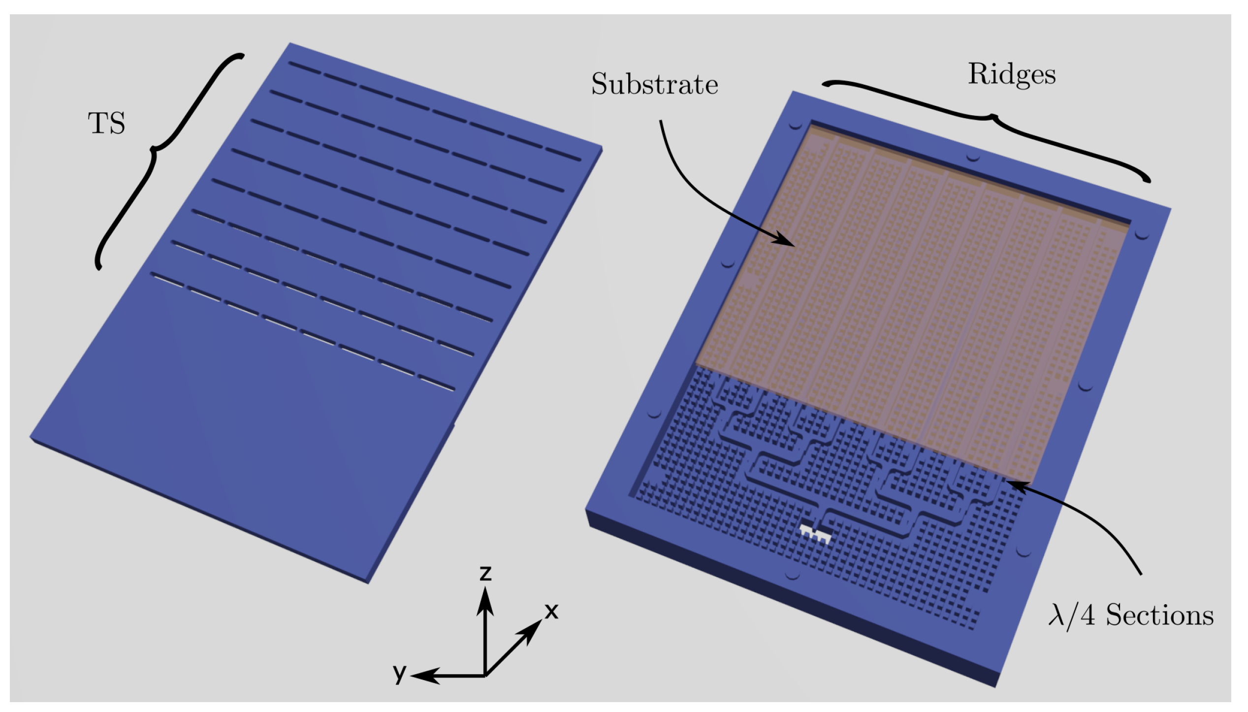
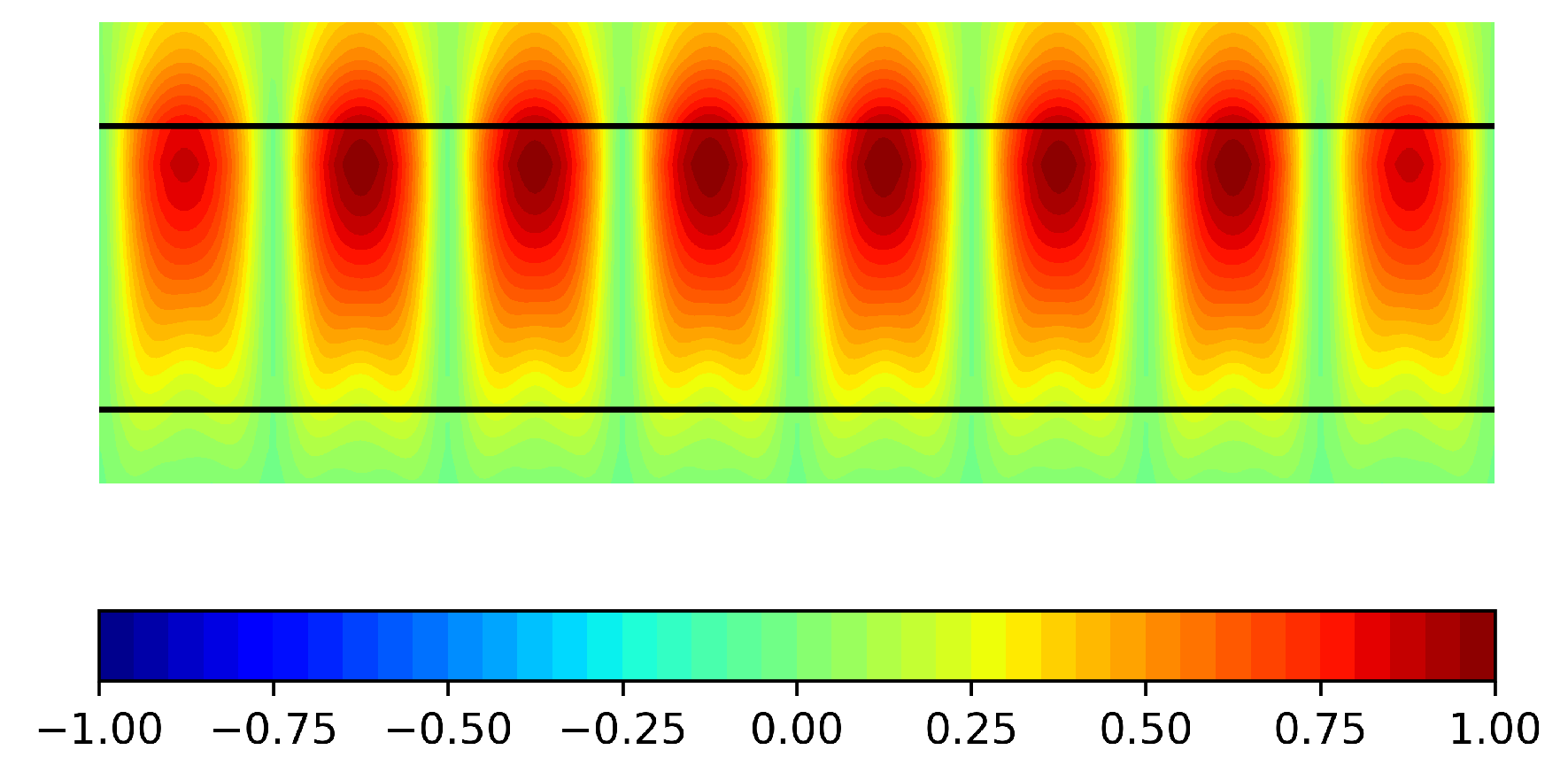
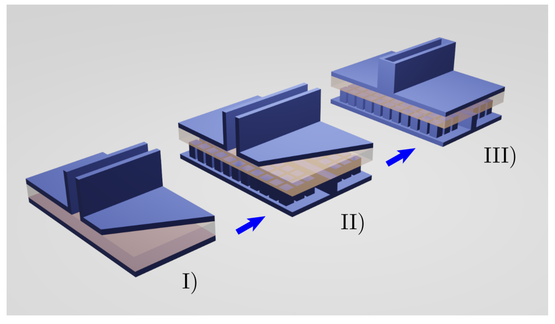
2. Antenna Design
2.1. Bed of Nails (BoN)
2.2. Corporate Feeding Network
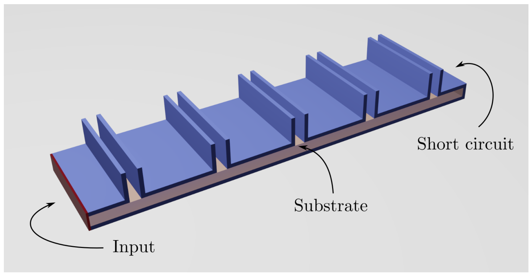
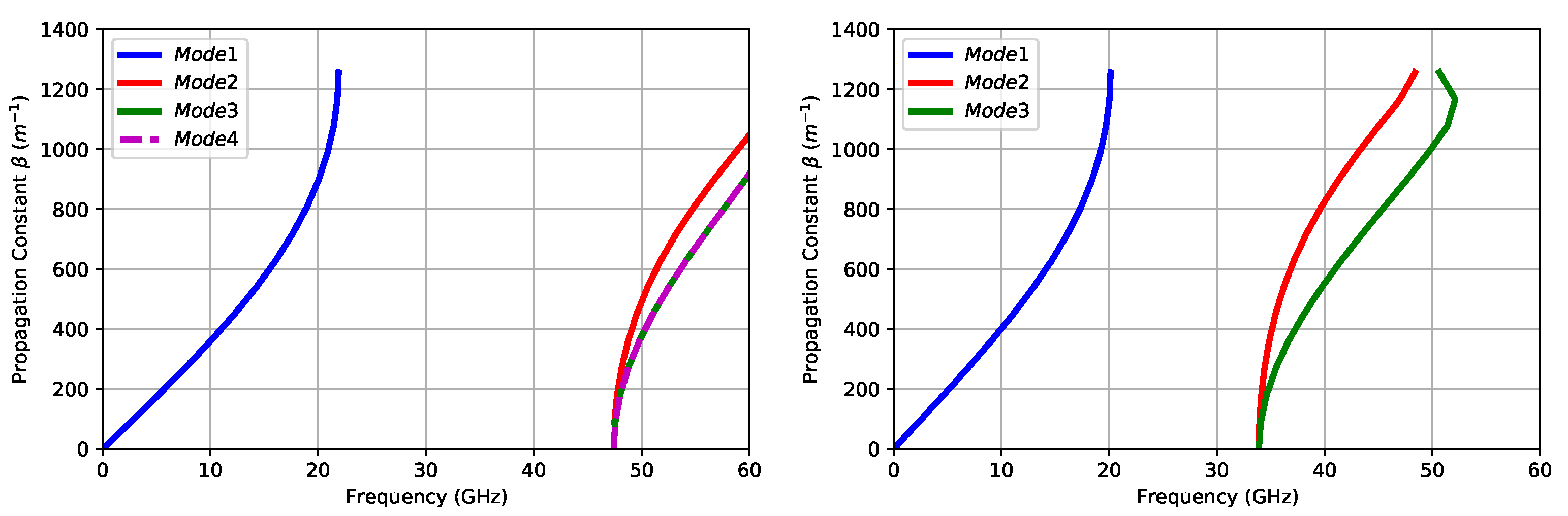
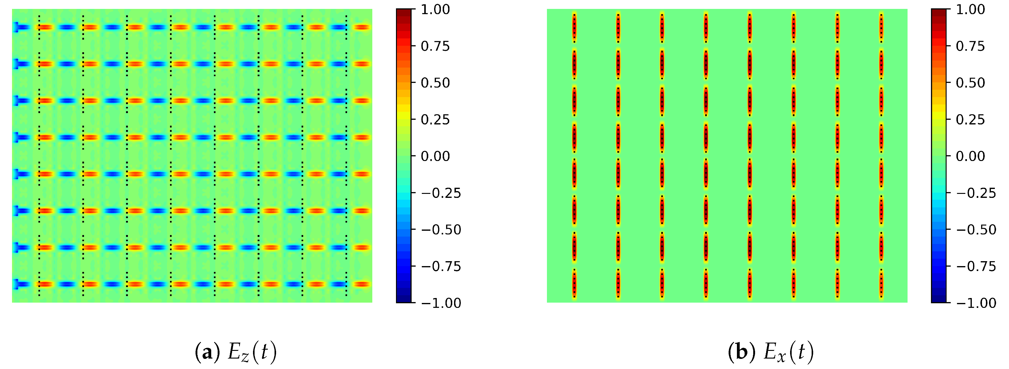
2.3. Radiating Structure
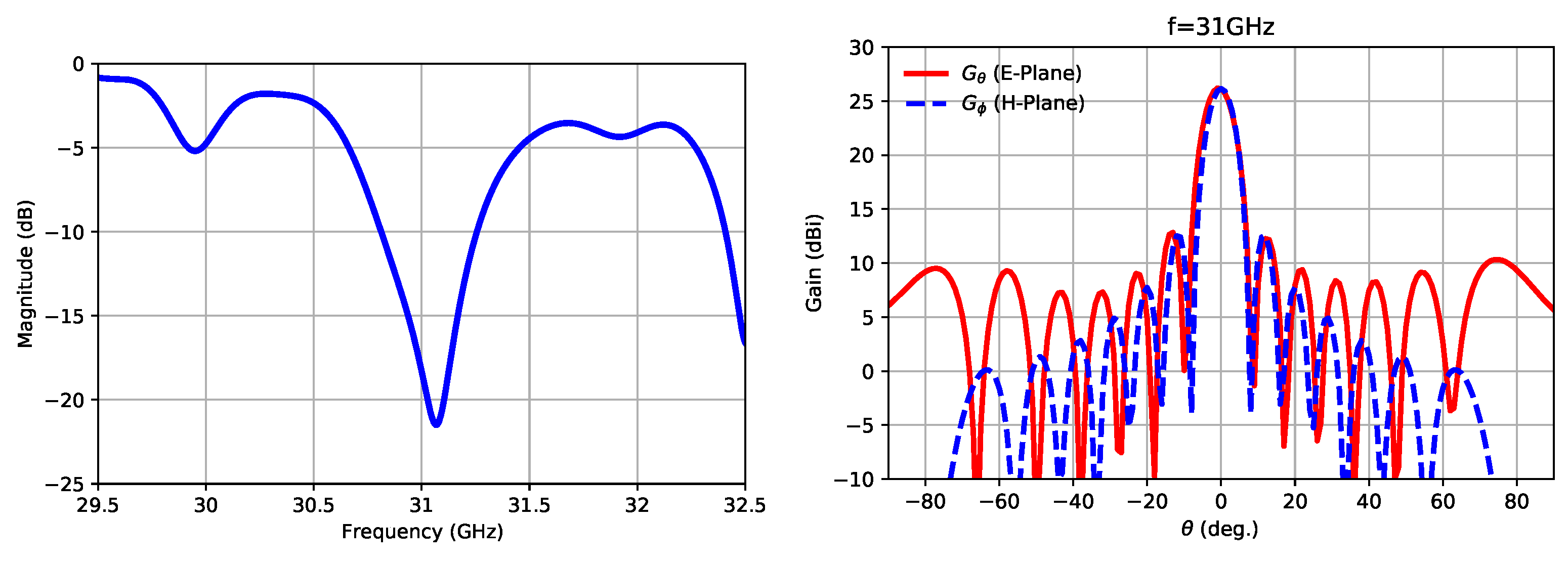
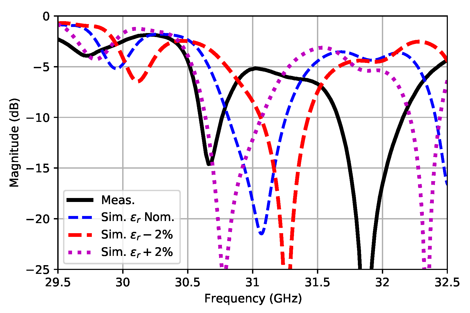
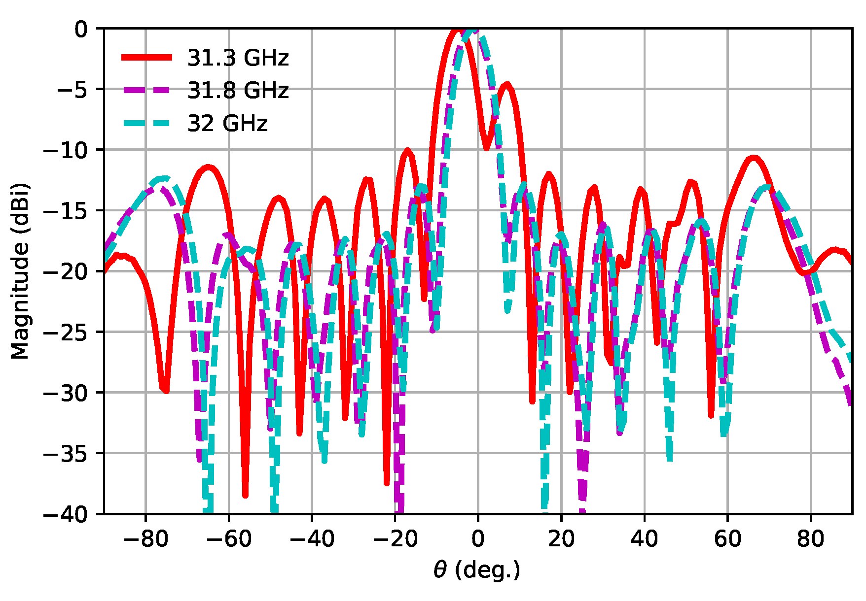
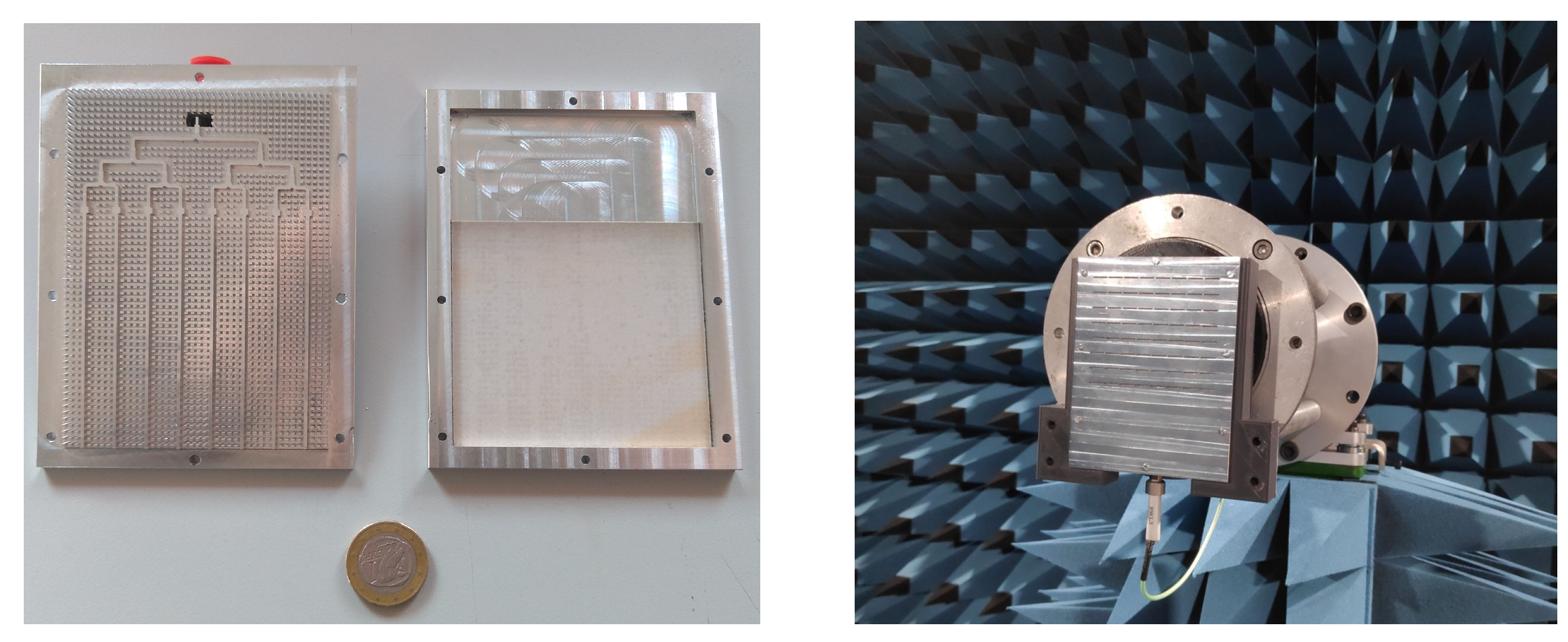
3. Experimental Results and Discussion
4. Conclusions and Future Work
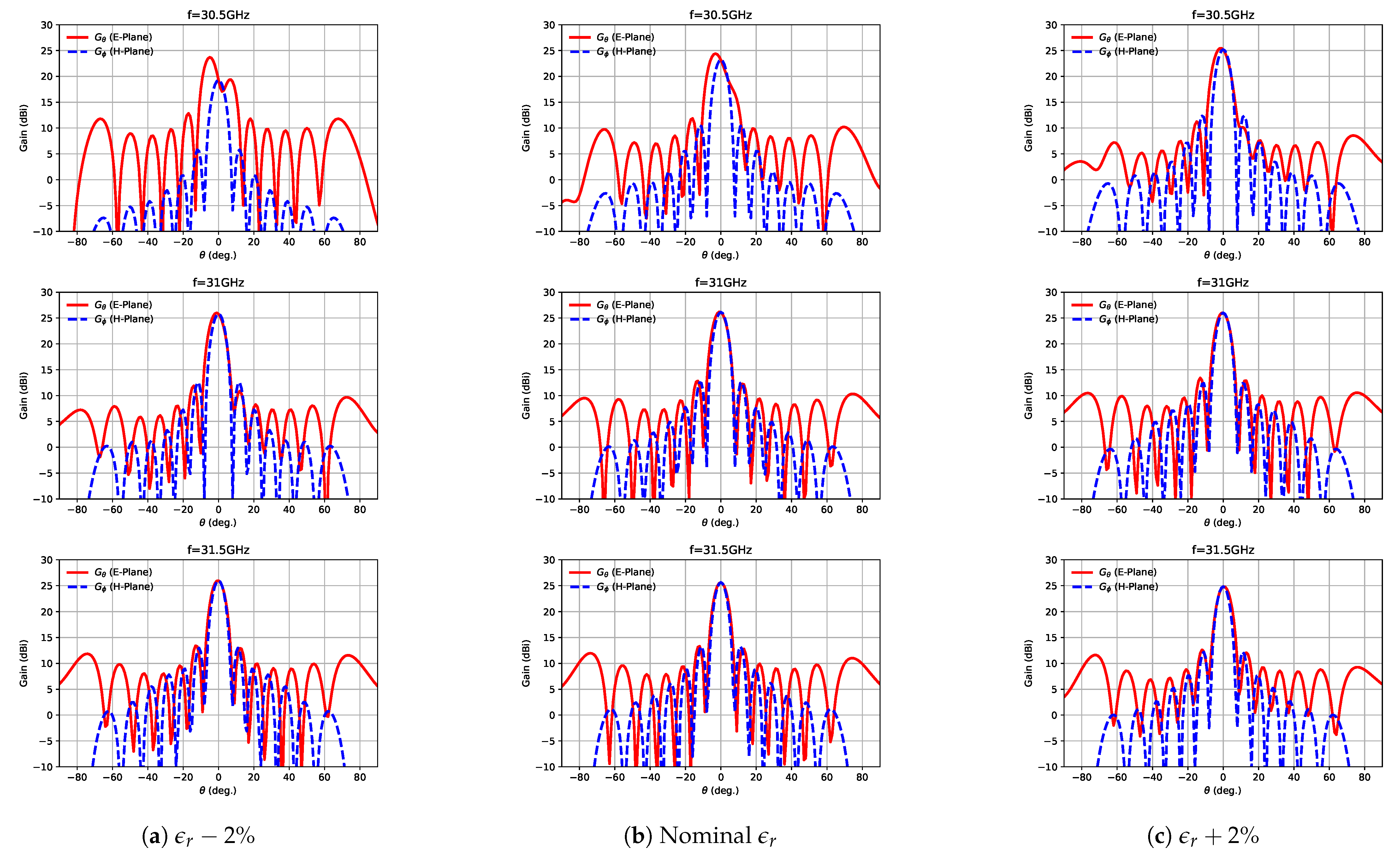
- The exact value of the substrate’s relative permittivity plays a critical role on the antenna performance, given that its resonant response is directly affected by this figure. As per commented before, when this value changes, the standing wave maxima positions move. This fact has a direct impact on the impedance bandwidth as well as on the E-plane radiation patterns, both in terms of the main lobe tilt and gain.
- There is a trade-off between the enhancement of the antenna directivity, achieved thanks to the good illumination obtained at the antenna aperture, and the insertion losses produced at the CFN that are used to feed the array. The evaluation of this trade-off is part of the work being conducted in ongoing research.
Author Contributions
Funding
Institutional Review Board Statement
Informed Consent Statement
Acknowledgments
Conflicts of Interest
Abbreviations
| BC | Boundary Condition |
| BoN | Bed of Nails |
| CFN | Corporate Feeding Network |
| CTS | Continuous Transverse Stub |
| PEC | Perfect Electric Conductor |
| PMC | Perfect Magnetic Conductor |
| PPW | Parallel-Plate Waveguide |
| RGW | Ridge Gap Waveguide |
| SLL | Side Lobe Level |
| TEM | Transverse Electro-Magnetic |
| TS | Transverse Stub |
References
- Milroy, W.W. The Continuous Transverse (CTS) array: Basic theory, experiment, and application. In Proceedings of the Antenna Applications Symposium, Monticello, IL, USA, 25–27 September 1991; Volume 1, pp. 253–283. [Google Scholar]
- Milroy, W.W. Continuous Transverse Stub Element Devices and Methods of Making Same. U.S. Patent US5266961A, 30 November 1991. [Google Scholar]
- Henderson, W.H.; Milroy, W.W. Wireless communication applications of the continuous transverse stub (CTS) array at microwave and millimeter wave frequencies. In Proceedings of the IEEE/ACES International Conference on Wireless Communications and Applied Computational Electromagnetics, Honolulu, HI, USA, 3–7 April 2005; pp. 253–256. [Google Scholar] [CrossRef]
- Pucci, E.; Zaman, A.U.; Rajo-Iglesias, E.; Kildal, P.S.; Kishk, A. Study of Q-factors of ridge and groove gap waveguide resonators. IET Microw. Antennas Propag. 2013, 7, 900–908. [Google Scholar] [CrossRef] [Green Version]
- Milroy, W.; Coppedge, S.; Ekmekji, A.; Hashemi-Yeganeh, S.; Buczeks, S. True-Time-Delay Feed Network for CTS Array. U.S. Patent 2006/0202899 A1, 14 September 2006. [Google Scholar]
- Ettorre, M.; Foglia Manzillo, F.; Casaletti, M.; Sauleau, R.; Capet, N. A compact and high-gain Ka-band multibeam continuous transverse stub antenna. In Proceedings of the 2015 IEEE International Symposium on Antennas and Propagation USNC/URSI National Radio Science Meeting, Vancouver, BC, Canada, 19–24 July 2015; pp. 671–672. [Google Scholar] [CrossRef]
- Kildal, P.S.; Zaman, A.; Rajo-Iglesias, E.; Alfonso, E.; Valero-Nogueira, A. Design and experimental verification of ridge gap waveguide in bed of nails for parallel-plate mode suppression. IET Microw. Antennas Propag. 2011, 5, 262–270. [Google Scholar] [CrossRef]
- Rajo-Iglesias, E.; Ferrando-Rocher, M.; Zaman, A.U. Gap Waveguide Technology for Millimeter-Wave Antenna Systems. IEEE Commun. Mag. 2018, 56, 14–20. [Google Scholar] [CrossRef] [Green Version]
- Kildal, P.; Alfonso, E.; Valero-Nogueira, A.; Rajo-Iglesias, E. Local Metamaterial-Based Waveguides in Gaps Between Parallel Metal Plates. IEEE Antennas Wirel. Propag. Lett. 2009, 8, 84–87. [Google Scholar] [CrossRef]
- Silveirinha, M.; Fernandes, C.; Costa, J. Electromagnetic Characterization of Textured Surfaces Formed by Metallic Pins. IEEE Trans. Antennas Propag. 2008, 56, 2695–2700. [Google Scholar] [CrossRef] [Green Version]
- Zaman, A.U.; Kildal, P.S. Slot antenna in ridge gap waveguide technology. In Proceedings of the 2012 6th European Conference on Antennas and Propagation (EUCAP), Prague, Czech Republic, 26–30 March 2012; pp. 3243–3244. [Google Scholar] [CrossRef] [Green Version]
- Liu, J.; Vosoogh, A.; Zaman, A.U.; Yang, J. A Slot Array Antenna With Single-Layered Corporate-Feed Based on Ridge Gap Waveguide in the 60 GHz Band. IEEE Trans. Antennas Propag. 2019, 67, 1650–1658. [Google Scholar] [CrossRef]
- Zarifi, D.; Farahbakhsh, A.; Zaman, A.U.; Kildal, P.S. Design and Fabrication of a High-Gain 60-GHz Corrugated Slot Antenna Array with Ridge Gap Waveguide Distribution Layer. IEEE Trans. Antennas Propag. 2016, 64, 2905–2913. [Google Scholar] [CrossRef] [Green Version]
- Benavides-Vazquez, J.; Vazquez-Roy, J.L.; Rajo-Iglesias, E. High-gain Resonant Continuous Transverse Stub Array Using Ridge Gap-Waveguide Technology. In Proceedings of the 2020 14th European Conference on Antennas and Propagation (EuCAP), Copenhagen, Denmark, 15–20 March 2020; pp. 1–4. [Google Scholar] [CrossRef]
- Domínguez, A.T.; González, J.M.F.; Alonso, J.M.I.; Sierra-Pérez, M. Design proposal for Ridge Gap Waveguide and comparison with other technologies in Ka to W bands. In Proceedings of the 2016 10th European Conference on Antennas and Propagation (EuCAP), Davos, Switzerland, 10–15 April 2016; pp. 1–5. [Google Scholar] [CrossRef] [Green Version]
- Zaman, A.U.; Kildal, P. Wide-Band Slot Antenna Arrays With Single-Layer Corporate-Feed Network in Ridge Gap Waveguide Technology. IEEE Trans. Antennas Propag. 2014, 62, 2992–3001. [Google Scholar] [CrossRef] [Green Version]
- Systèmes, D. Electromagnetic Simulation Solvers. 2021. Available online: https://www.3ds.com/products-services/simulia/products/cst-studio-suite/solvers/ (accessed on 15 August 2021).
- You, Q.; Lu, Y.; You, Y.; Wang, Y.; Hao, Z.C.; Huang, J. Wideband Full-Corporate-Feed Waveguide Continuous Transverse Stub Antenna Array. IEEE Access 2018, 6, 76673–76681. [Google Scholar] [CrossRef]
- Ettorre, M.; Manzillo, F.F.; Casaletti, M.; Sauleau, R.; Le Coq, L.; Capet, N. Continuous Transverse Stub Array for Ka-Band Applications. IEEE Trans. Antennas Propag. 2015, 63, 4792–4800. [Google Scholar] [CrossRef]
- Potelon, T.; Ettorre, M.; Le Coq, L.; Bateman, T.; Francey, J.; Lelaidier, D.; Seguenot, E.; Devillers, F.; Sauleau, R. A Low-Profile Broadband 32-Slot Continuous Transverse Stub Array for Backhaul Applications in E -Band. IEEE Trans. Antennas Propag. 2017, 65, 6307–6316. [Google Scholar] [CrossRef]


| Parameter | Parameter Description | Value (mm) |
|---|---|---|
| Pin height | 2.42 | |
| s | Pin side width | 1 |
| p | Pin period | 1.75 |
| Separation between a ridge and its adjacent pin column | 1.75 | |
| Height of the substrate gap | 1.27 | |
| Height of the air gap | 0.5 |
| Parameter | Parameter Description | Value (mm) |
|---|---|---|
| Ridge width of the WR28 transition | 0.75 | |
| ridge impedance transformers width | 1.5 | |
| Corporate feeding ridges width | 1 | |
| Air gap at the feeding network | 0.5 | |
| Substrate height at the radiating section | 1.27 | |
| TS length | 2 | |
| TS width | 0.9 | |
| Distance between ridges | 8.75 | |
| Distance between TS | 8 | |
| Matching section length (dielectric discontinuity) | 1.69 | |
| Matching section width (dielectric discontinuity) | 2.25 |
| Parameter | Parameter Description | Simulation 31 GHz | Measurement 31.8 GHz |
|---|---|---|---|
| B | Matching bandwidth ( > 10 dB) | 446 MHz | 517 MHz |
| G | Antenna gain | 26.2 dB | 24.5 dB |
| E-plane angular width (−3 dB) | 7.8 | ||
| H-plane angular width (−3 dB) | 7 | ||
| E-plane SLL | −13.2 dB | −13.1 dB | |
| H-plane SLL | −13.8 dB | −8.7 dB |
Publisher’s Note: MDPI stays neutral with regard to jurisdictional claims in published maps and institutional affiliations. |
© 2021 by the authors. Licensee MDPI, Basel, Switzerland. This article is an open access article distributed under the terms and conditions of the Creative Commons Attribution (CC BY) license (https://creativecommons.org/licenses/by/4.0/).
Share and Cite
Benavides-Vazquez, J.; Vazquez-Roy, J.-L.; Rajo-Iglesias, E. On the Use of Ridge Gap Waveguide Technology for the Design of Transverse Stub Resonant Antenna Arrays. Sensors 2021, 21, 6590. https://doi.org/10.3390/s21196590
Benavides-Vazquez J, Vazquez-Roy J-L, Rajo-Iglesias E. On the Use of Ridge Gap Waveguide Technology for the Design of Transverse Stub Resonant Antenna Arrays. Sensors. 2021; 21(19):6590. https://doi.org/10.3390/s21196590
Chicago/Turabian StyleBenavides-Vazquez, Javier, Jose-Luis Vazquez-Roy, and Eva Rajo-Iglesias. 2021. "On the Use of Ridge Gap Waveguide Technology for the Design of Transverse Stub Resonant Antenna Arrays" Sensors 21, no. 19: 6590. https://doi.org/10.3390/s21196590
APA StyleBenavides-Vazquez, J., Vazquez-Roy, J.-L., & Rajo-Iglesias, E. (2021). On the Use of Ridge Gap Waveguide Technology for the Design of Transverse Stub Resonant Antenna Arrays. Sensors, 21(19), 6590. https://doi.org/10.3390/s21196590