
A Heterogeneous RISC-V Processor for Efficient DNN Application in Smart Sensing System

 and
and
Abstract
:1. Introduction
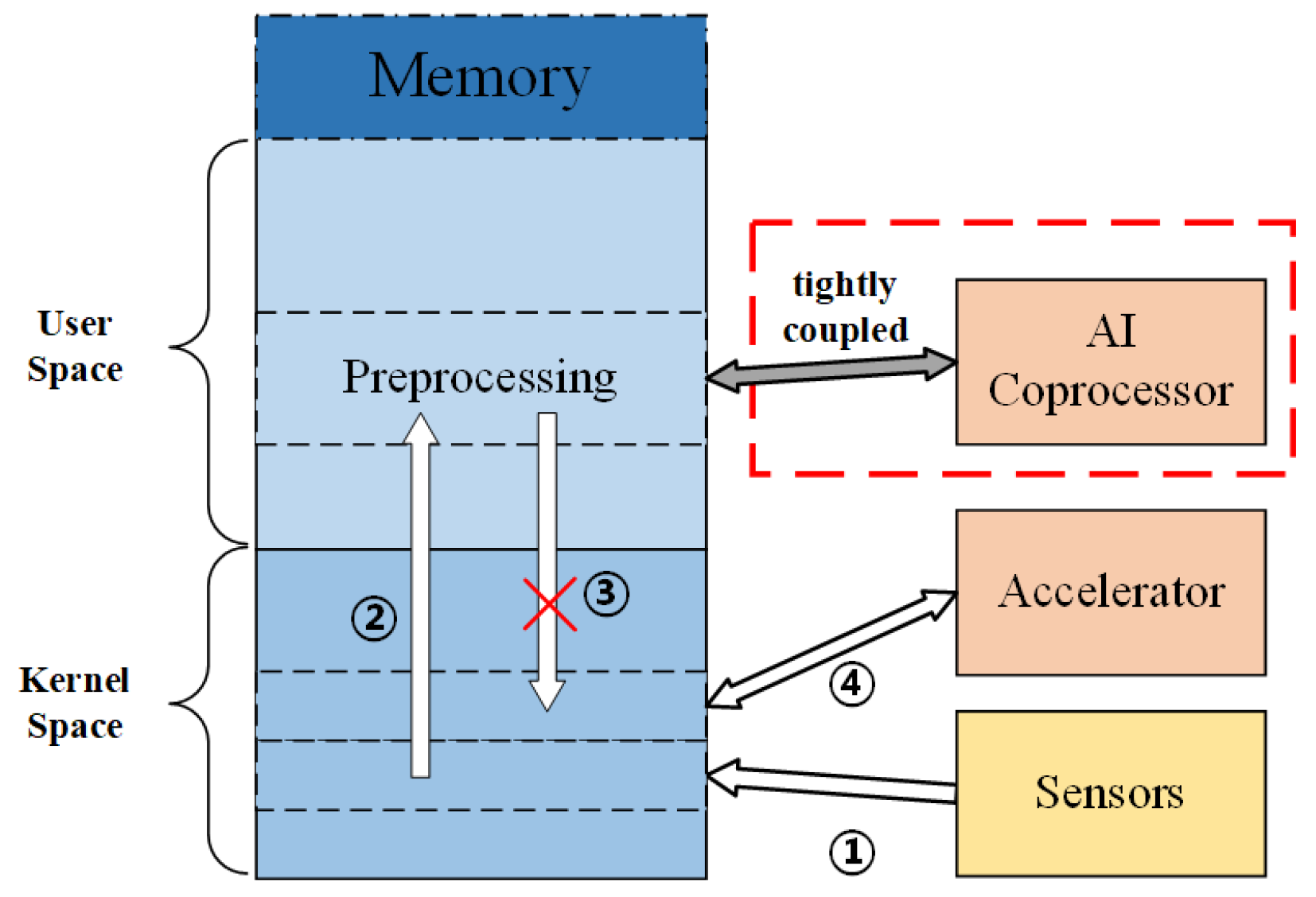
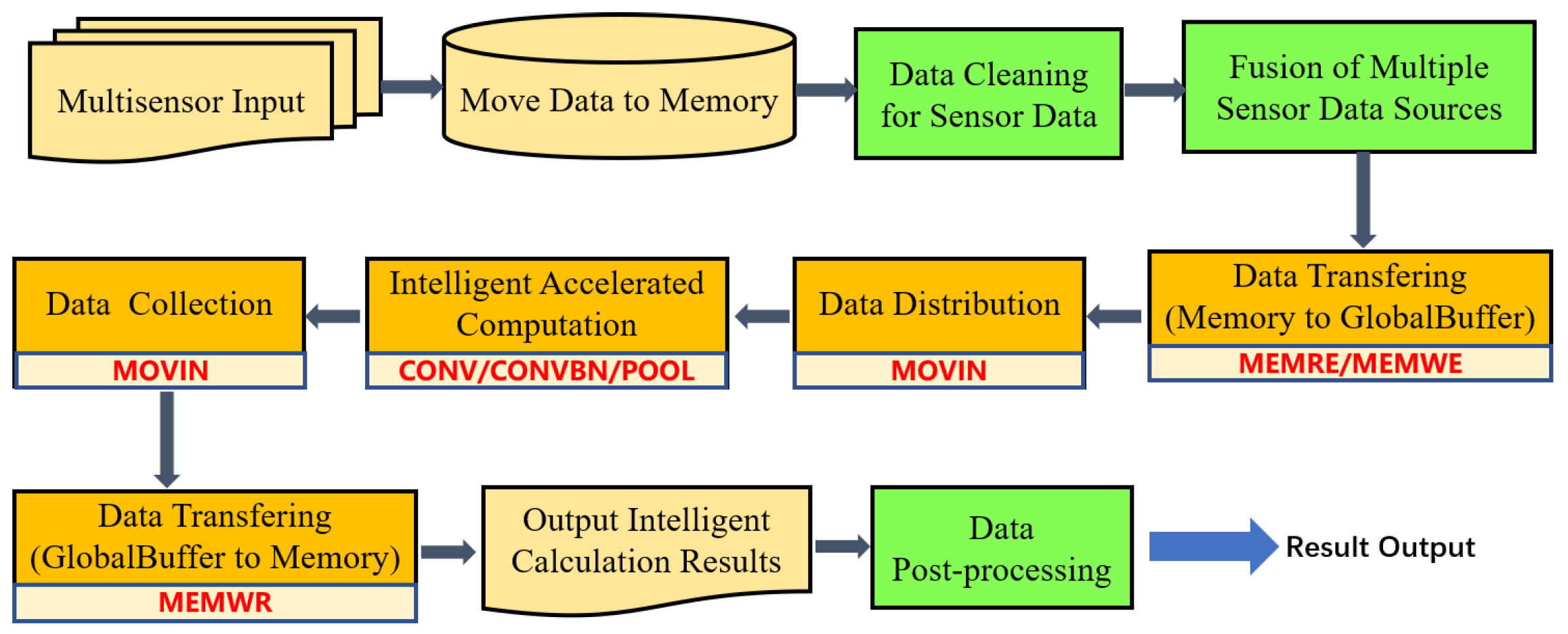
2. Motivation
- We design a mapping method to realize the deployment of different dataflows, thereby satisfying the requirements for configuration flexibility;
- We propose a lightweight tightly coupled architecture, VLIW ISA based SIMD architecture (VISA), achieving a balanced performance metrics including low power consumption, low latency and flexible configuration;
- We develop a RISC-V dedicated intelligent enhanced VLIW instruction subset to maintain various dataflows and support different DNN calculations.
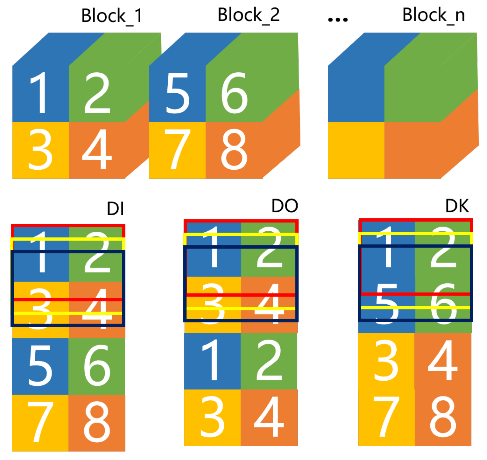
3. Mapping Method of Data Flow
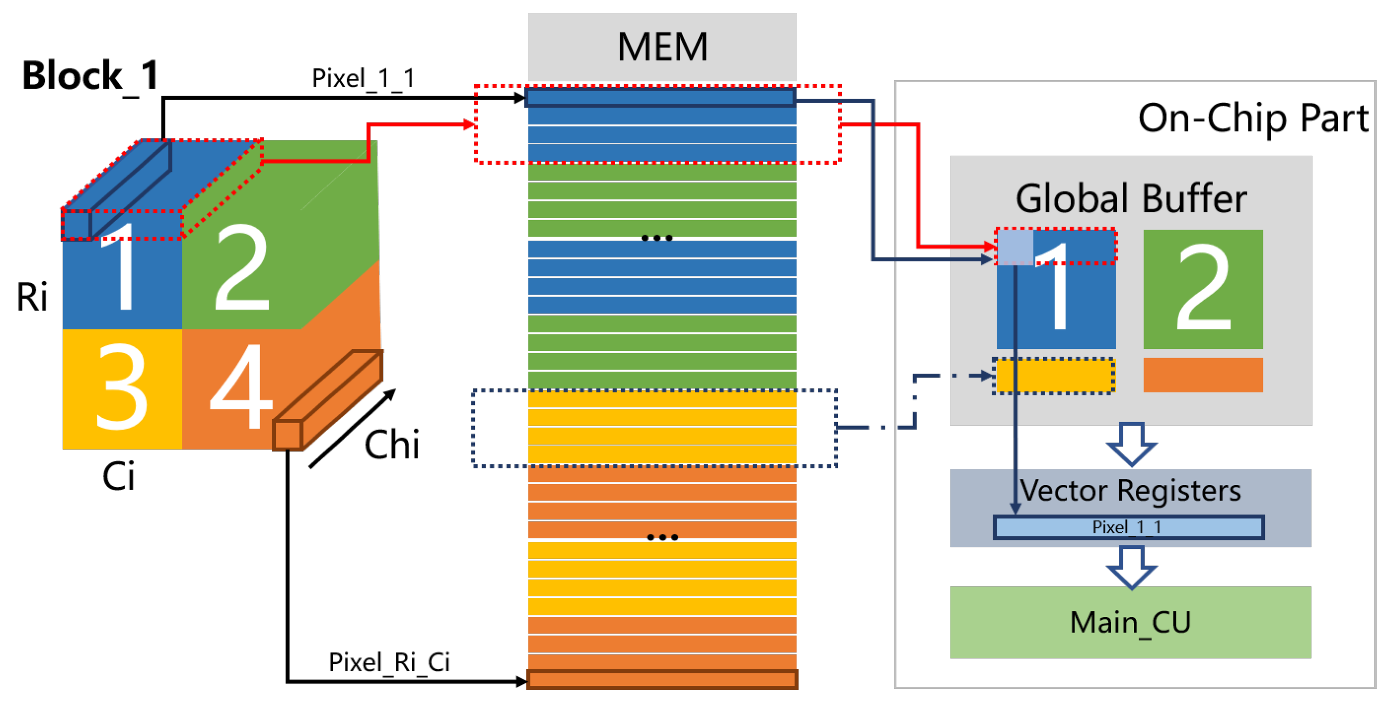
3.1. Analysis of Calculation Consistency
3.1.1. Convolution
3.1.2. Batch Normalization
3.2. Data Flow Scheduling Analysis
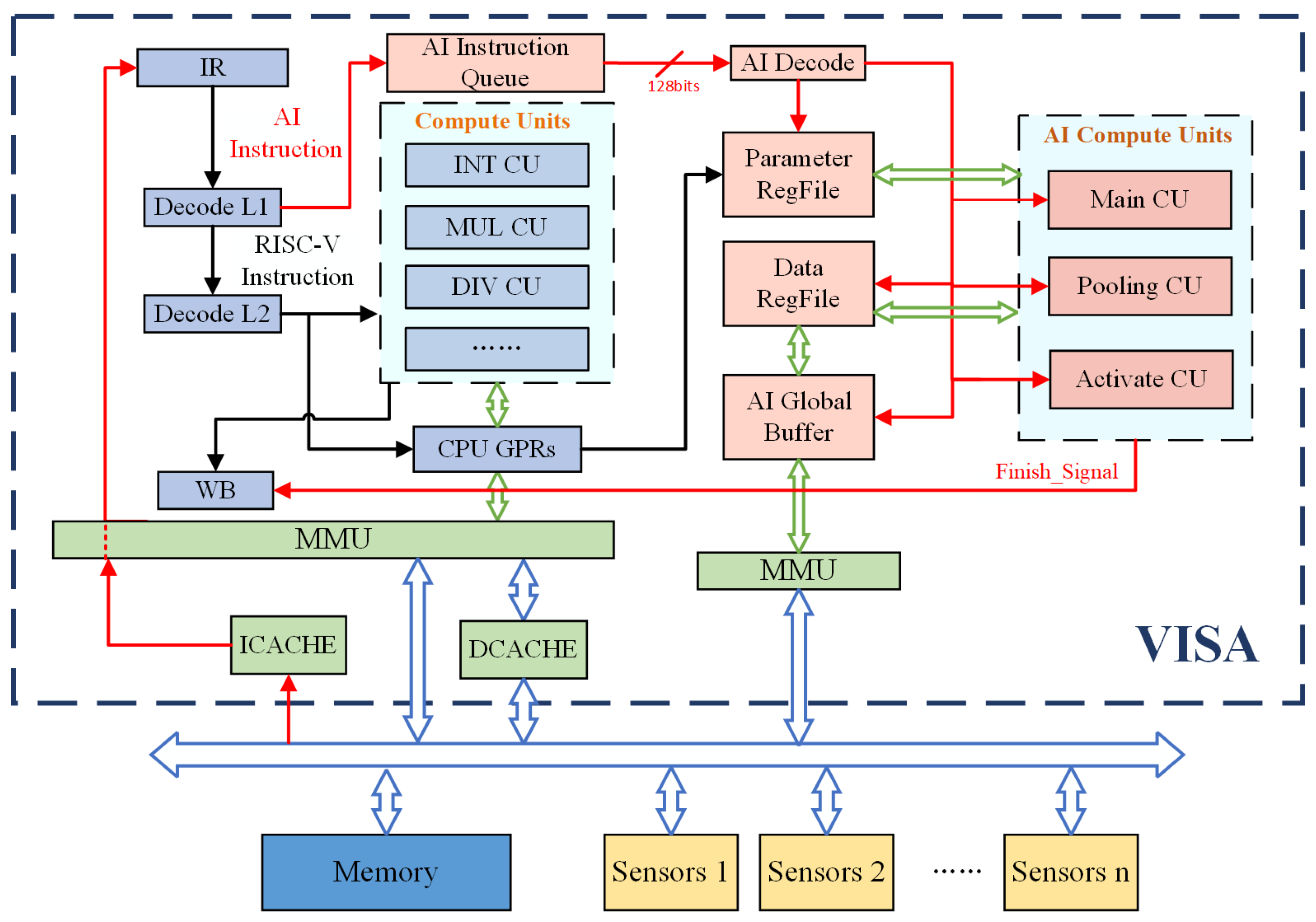
4. VISA: A Lightweight Pipeline Integrated Deep Learning Architecture
4.1. Architecture Overview
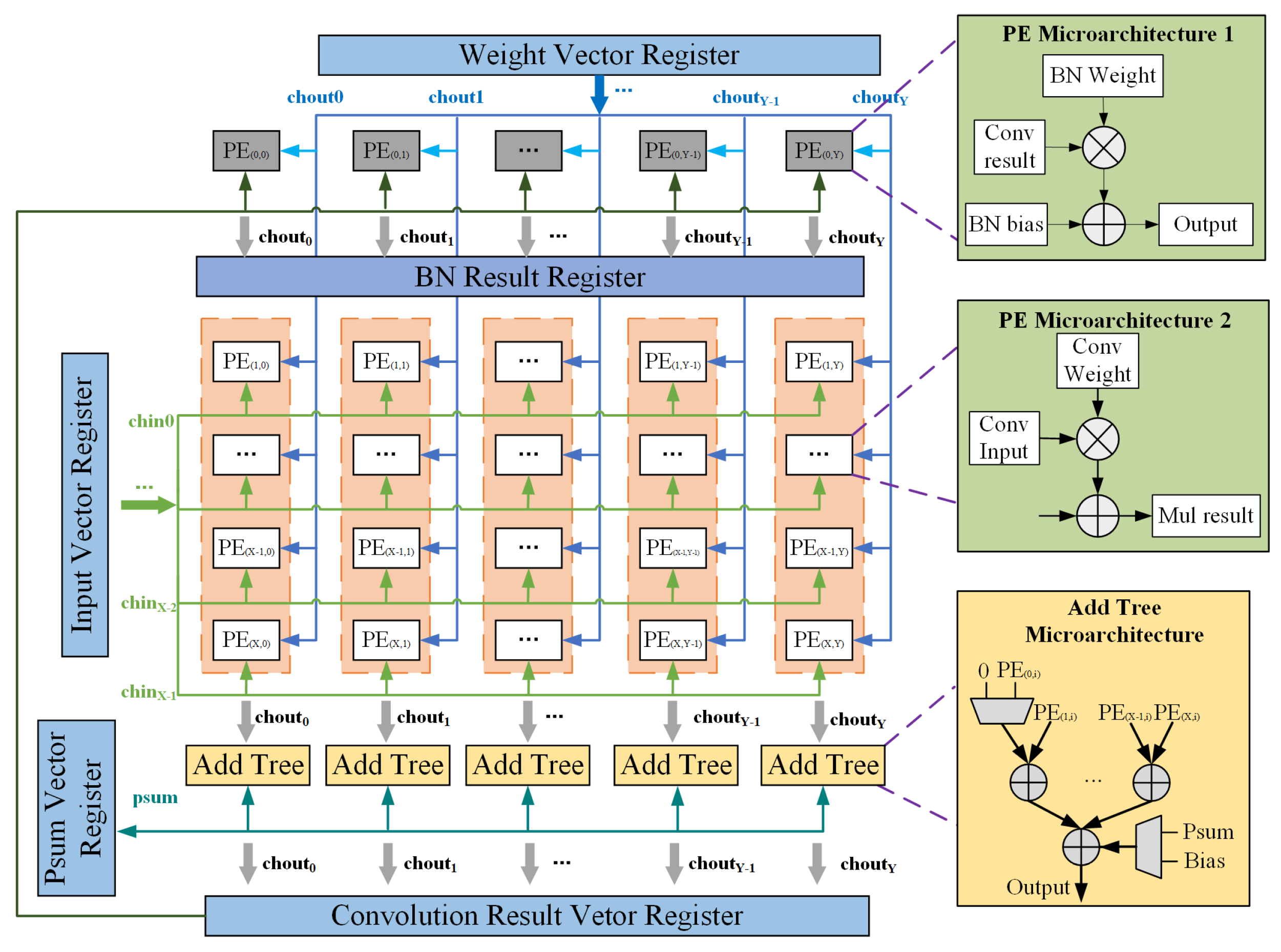
4.2. Microarchitecture of SIMD Computing Unit
- Send the data corresponding to chin 0∼7 of the window_pixel (0,0) to 8 rows of PEs, and send the data corresponding to window_pixel (0,0) of chin 0∼7 which are corresponding to chout 0∼7 to PEs in rows 0∼7 and columns 0∼7, respectively. Calculate the partial sum of chout 0∼7, and then add it to the bias value in the bias register, that is, use bias as the initial part;
- Send the data corresponding to chin 0∼7 of the window_pixel (0,1) to 8 rows of PEs, and send the data corresponding to window_pixel (0,0) of chin 0∼7 which are corresponding to chout 0∼7 to PEs in rows 0∼7 and columns 0∼7, respectively. Calculate the partial sum of chout 0∼7, and then add it to the previous partial sums;
- In this way, until the sending of the data corresponding to chin 0∼7 of the window_pixel (2,2) to 8 rows of PEs, and the sending the data corresponding to window_pixel (2,2) of chin 0∼7 which are corresponding to chout0∼7 to PEs in rows 0∼7 and columns 0∼7, respectively. The MAC calculation results of a convolution window and 8 input channels are obtained.
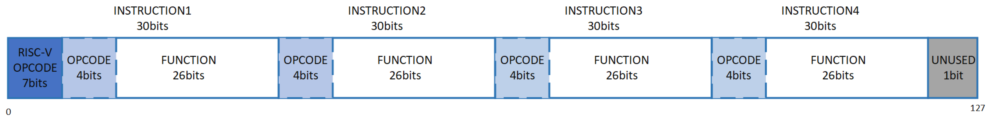
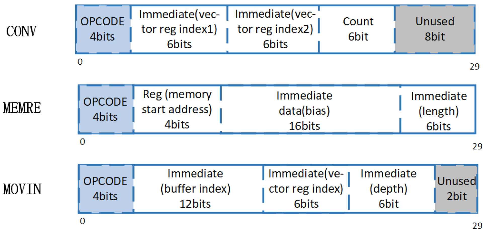
5. VLIW Instruction Set Architecture
5.1. VLIW Instruction Format
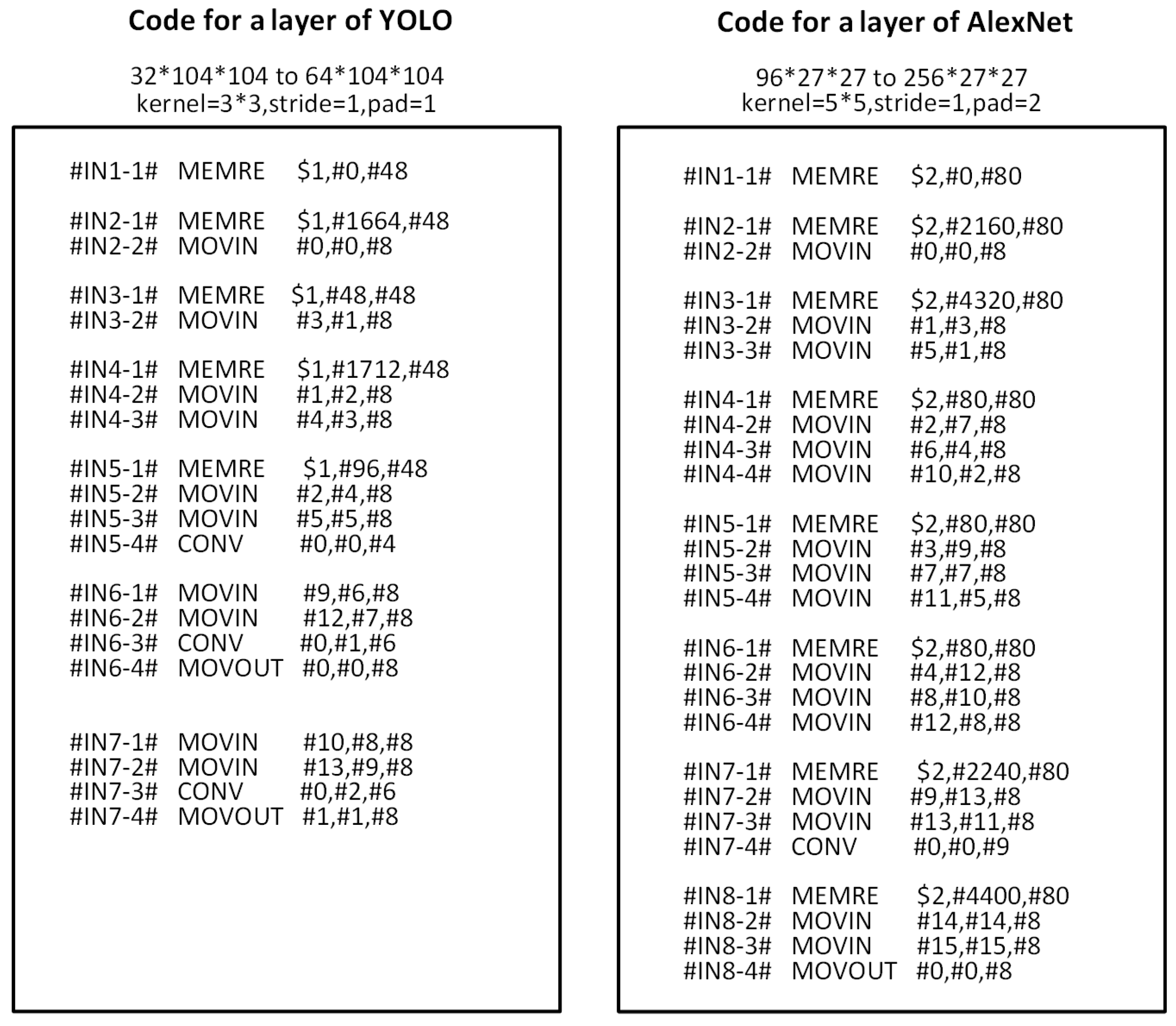
5.2. Neural Network Application Deployment
5.2.1. Scheduling of VLIW Instructions
5.2.2. Program Framework
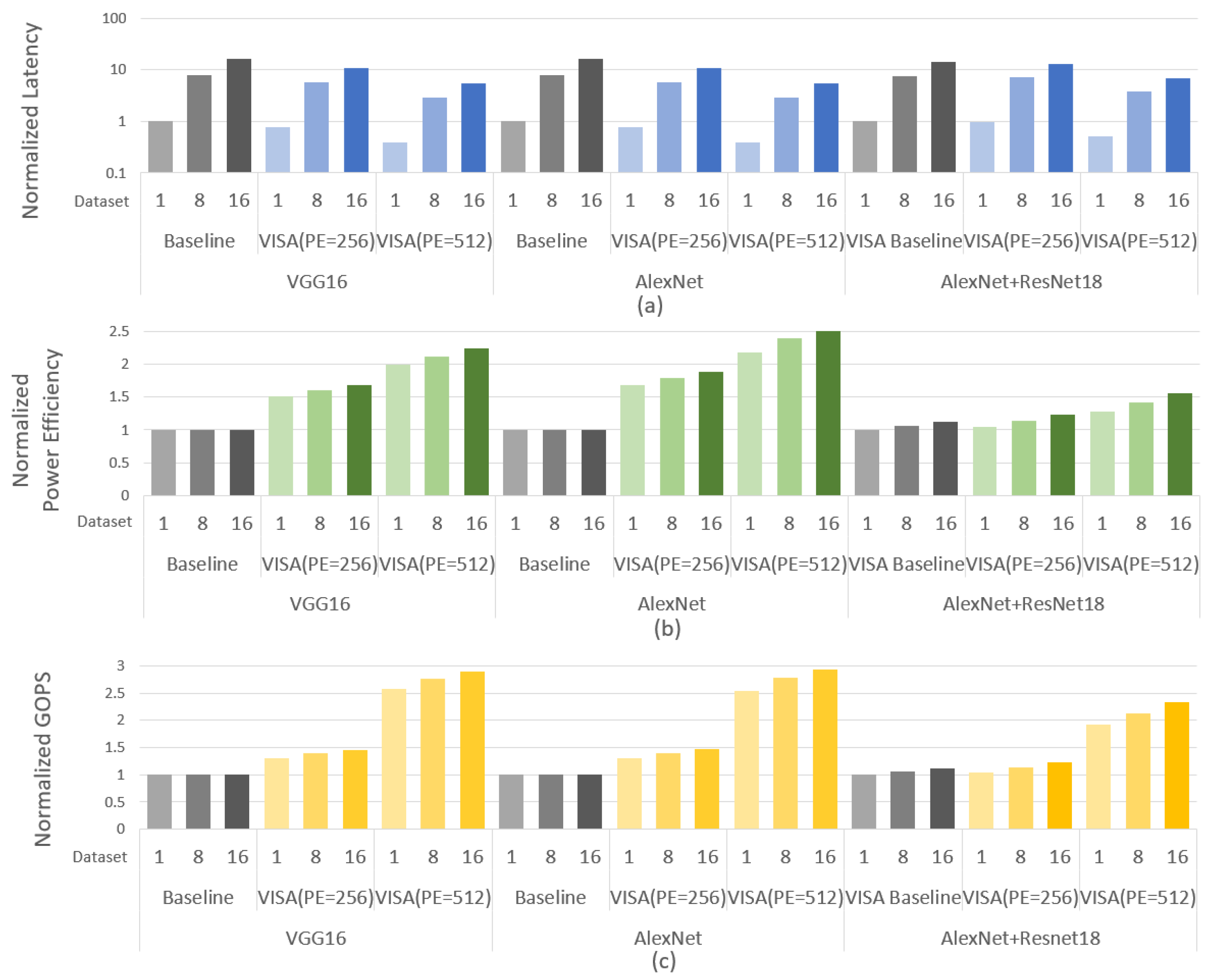
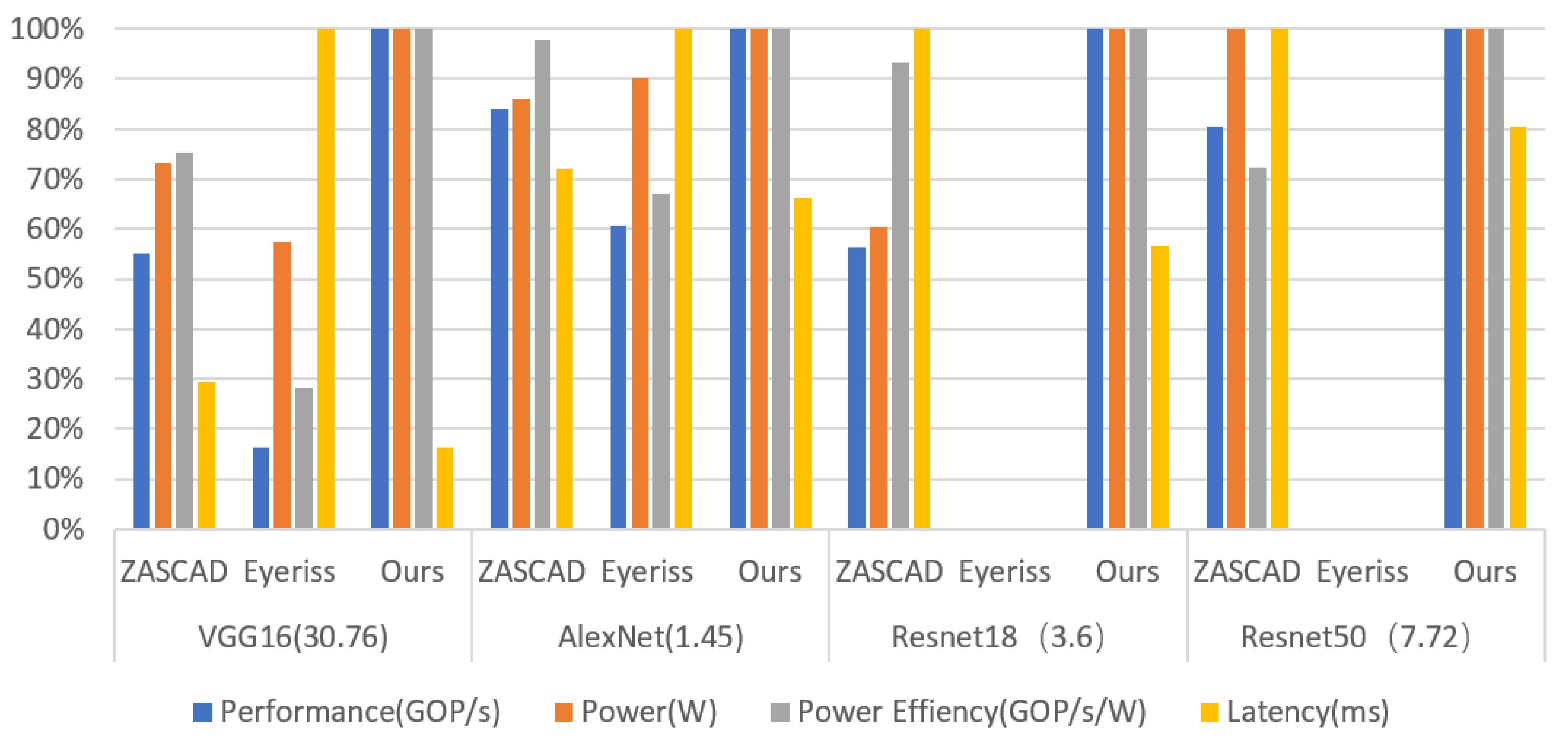
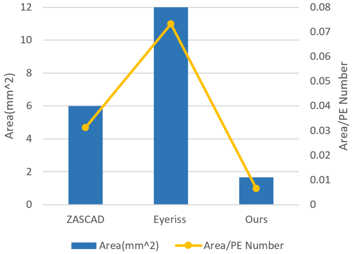
6. Experimental Evaluation
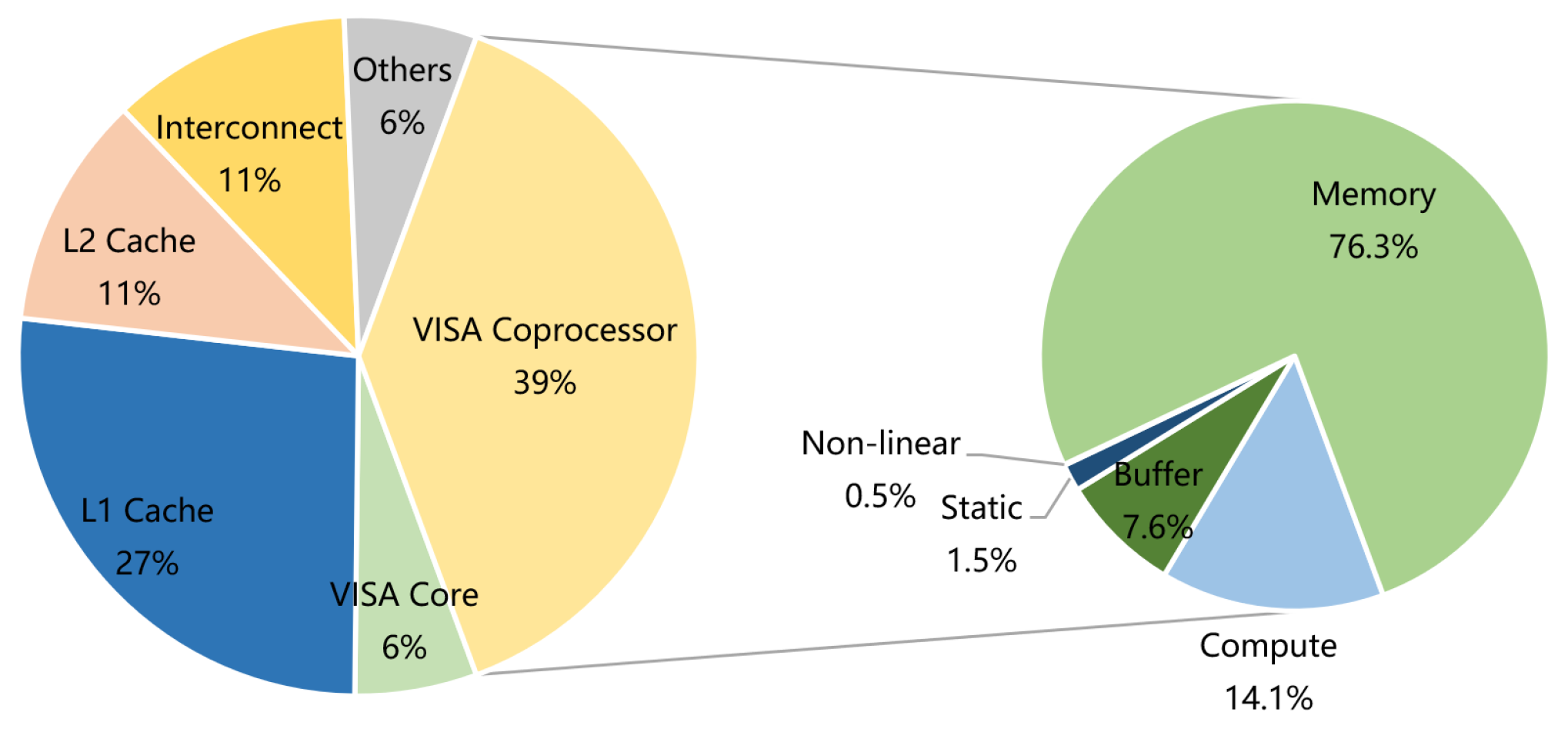
6.1. Design Synthesis and Resource Analysis
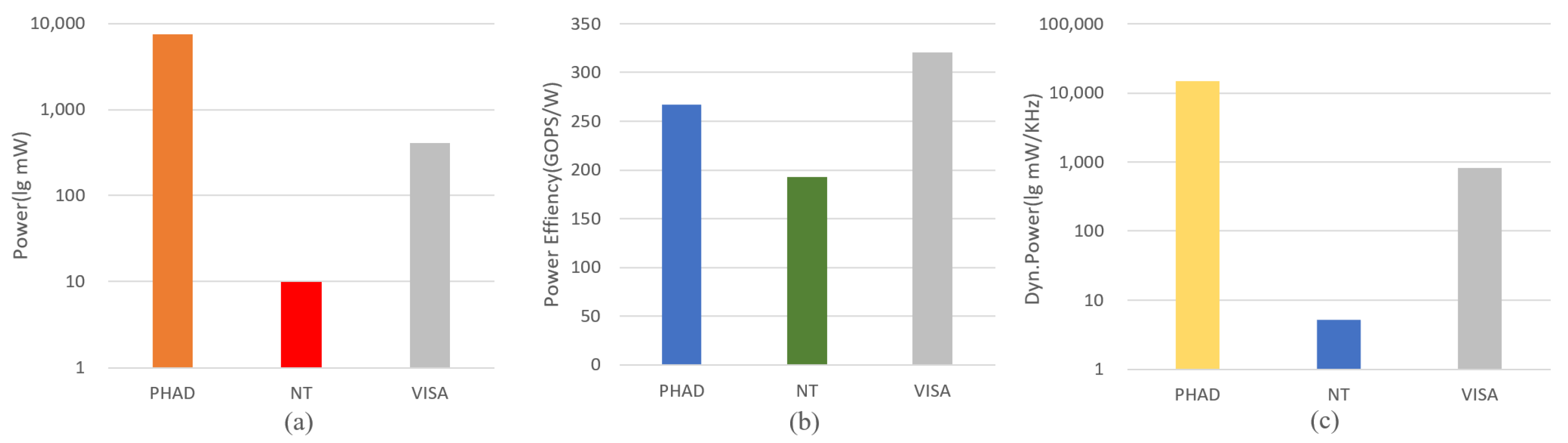
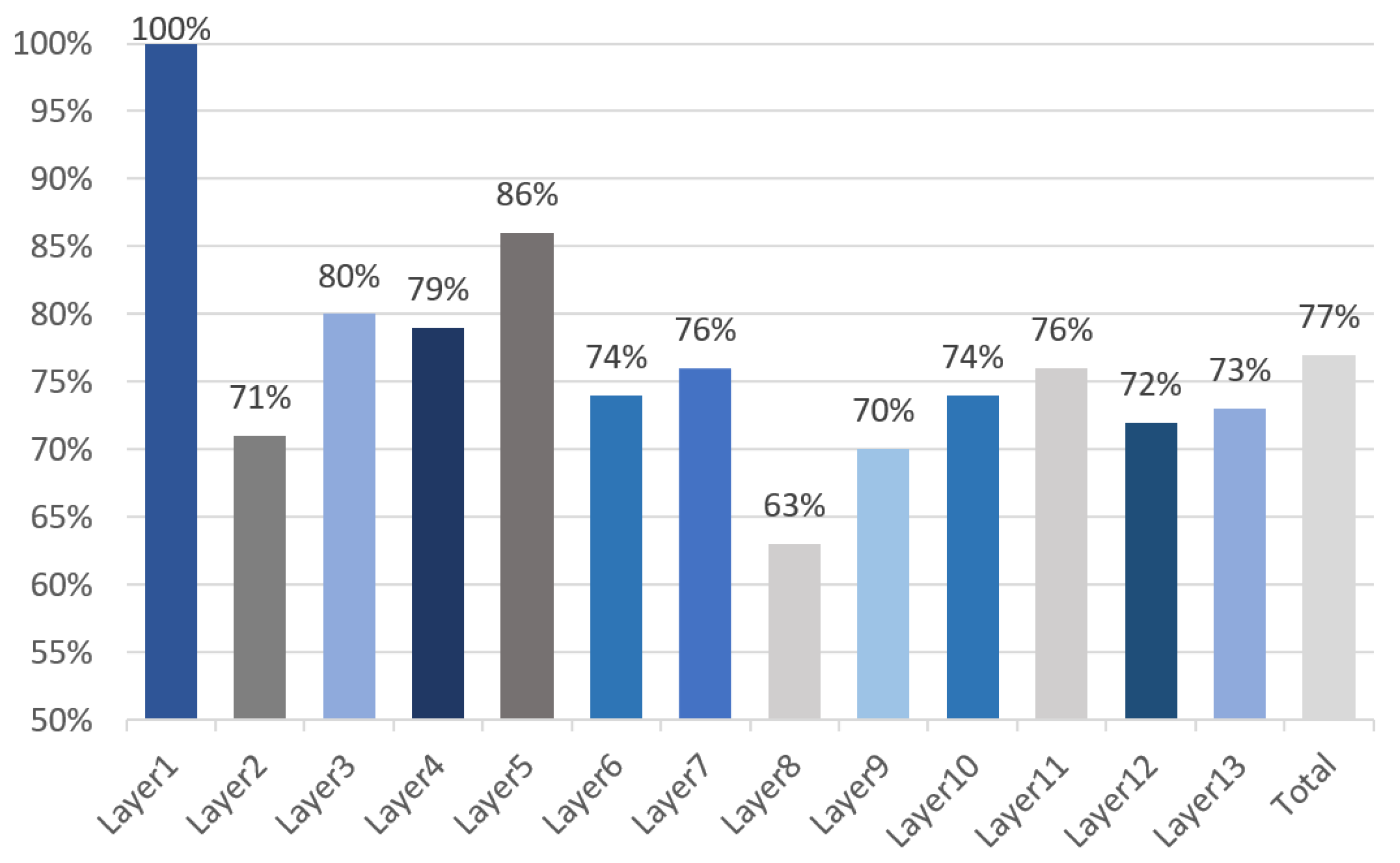
6.2. Performance Evaluation
7. Conclusions
Author Contributions
Funding
Institutional Review Board Statement
Informed Consent Statement
Acknowledgments
Conflicts of Interest
References
- Wang, M.; Fan, X.; Zhang, W.; Zhu, T.; Yao, T.; Ding, H.; Wang, D. Balancing memory-accessing and computing over sparse DNN accelerator via efficient data packaging. J. Syst. Archit. 2021, 117, 102094. [Google Scholar] [CrossRef]
- Chen, Y.; Krishna, T.; Emer, J.; Sze, V. 14.5 Eyeriss: An energy-efficient reconfigurable accelerator for deep convolutional neural networks. In Proceedings of the 2016 IEEE International Solid-State Circuits Conference (ISSCC), San Francisco, CA, USA, 31 January–4 February 2016; pp. 262–263. [Google Scholar] [CrossRef] [Green Version]
- Chen, Y.; Luo, T.; Liu, S.; Zhang, S.; He, L.; Wang, J.; Li, L.; Chen, T.; Xu, Z.; Sun, N.; et al. DaDianNao: A Machine-Learning Supercomputer. In Proceedings of the 2014 47th Annual IEEE/ACM International Symposium on Microarchitecture, Cambridge, UK, 13–17 December 2014; pp. 609–622. [Google Scholar] [CrossRef]
- Liu, D.; Chen, T.; Liu, S.; Zhou, J.; Zhou, S.; Teman, O.; Feng, X.; Zhou, X.; Chen, Y. PuDianNao: A Polyvalent Machine Learning Accelerator. SIGARCH Comput. Archit. News 2015, 43, 369–381. [Google Scholar] [CrossRef]
- Du, Z.; Fasthuber, R.; Chen, T.; Ienne, P.; Li, L.; Luo, T.; Temam, O. ShiDianNao: Shifting vision processing closer to the sensor. In Proceedings of the 2015 ACM/IEEE 42nd Annual International Symposium on Computer Architecture (ISCA), Portland, OR, USA, 13–17 June 2015; pp. 92–104. [Google Scholar] [CrossRef]
- Liu, S.; Du, Z.; Tao, J.; Han, D.; Luo, T.; Xie, Y.; Chen, Y.; Chen, T. Cambricon: An instruction set architecture for neural networks. In Proceedings of the 43rd International Symposium on Computer Architecture (ISCA’16), Seoul, Korea, 18–22 June 2016; pp. 393–405. [Google Scholar] [CrossRef] [Green Version]
- Zhang, S.; Du, Z.; Zhang, L.; Lan, H.; Liu, S.; Li, L.; Guo, Q.; Chen, T.; Chen, Y. Cambricon-x: An accelerator for sparse neural networks. In Proceedings of the 49th Annual IEEE/ACM International Symposium on Microarchitecture (MICRO-49), Taipei, Taiwan, 15–19 October 2016; pp. 1–12. [Google Scholar]
- Parashar, A.; Rhu, M.; Mukkara, A.; Puglielli, A.; Venkatesan, R.; Khailany, B.; Emer, J.S.; Keckler, S.W.; Dally, W.J. SCNN: An accelerator for compressed-sparse convolutional neural networks. In Proceedings of the 2017 ACM/IEEE 44th Annual International Symposium on Computer Architecture (ISCA), Toronto, ON, Canada, 24–28 June 2017; pp. 27–40. [Google Scholar] [CrossRef]
- Sun, F.; Wang, C.; Gong, L.; Xu, C.; Zhang, Y.; Lu, Y.; Li, X.; Zhou, X. A High-Performance Accelerator for Large-Scale Convolutional Neural Networks. In Proceedings of the 2017 IEEE International Symposium on Parallel and Distributed Processing with Applications and 2017 IEEE International Conference on Ubiquitous Computing and Communications (ISPA/IUCC), Guangzhou, China, 12–15 December 2017; pp. 622–629. [Google Scholar] [CrossRef]
- Song, Z.; Fu, B.; Wu, F.; Jiang, Z.; Jiang, L.; Jing, N.; Liang, X. DRQ: Dynamic Region-based Quantization for Deep Neural Network Acceleration. In Proceedings of the 2020 ACM/IEEE 47th Annual International Symposium on Computer Architecture (ISCA), Valencia, Spain, 30 May–3 June 2020; pp. 1010–1021. [Google Scholar] [CrossRef]
- Ottavi, G.; Garofalo, A.; Tagliavini, G.; Conti, F.; Benini, L.; Rossi, D. A Mixed-Precision RISC-V Processor for Extreme-Edge DNN Inference. In Proceedings of the 2020 IEEE Computer Society Annual Symposium on VLSI (ISVLSI), Limassol, Cyprus, 6–8 July 2020; pp. 512–517. [Google Scholar] [CrossRef]
- Bruschi, N.; Garofalo, A.; Conti, F.; Tagliavini, G.; Rossi, D. Enabling mixed-precision quantized neural networks in extreme-edge devices. In Proceedings of the 17th ACM International Conference on Computing Frontiers (CF’20), Siena, Italy, 15–17 May 2020; Association for Computing Machinery: New York, NY, USA, 2020; pp. 217–220. [Google Scholar] [CrossRef]
- Zhao, B.; Li, J.; Pan, H.; Wang, M. A High-Performance Reconfigurable Accelerator for Convolutional Neural Networks. In Proceedings of the 3rd International Conference on Multimedia Systems and Signal Processing (ICMSSP’18), Shenzhen China, 28–30 April 2018; Association for Computing Machinery: New York, NY, USA, 2018; pp. 150–155. [Google Scholar] [CrossRef]
- Kong, A.; Zhao, B. A High Efficient Architecture for Convolution Neural Network Accelerator. In Proceedings of the 2019 2nd International Conference on Intelligent Autonomous Systems (ICoIAS), Singapore, 28 Februay–2 March 2019; pp. 131–134. [Google Scholar] [CrossRef]
- Xie, W.; Zhang, C.; Zhang, Y.; Hu, C.; Jiang, H.; Wang, Z. An Energy-Efficient FPGA-Based Embedded System for CNN Application. In Proceedings of the 2018 IEEE International Conference on Electron Devices and Solid State Circuits (EDSSC), Shenzhen, China, 6–8 June 2018; pp. 1–2. [Google Scholar] [CrossRef]
- Choi, J.; Srinivasa, S.; Tanabe, Y.; Sampson, J.; Narayanan, V. A Power-Efficient Hybrid Architecture Design for Image Recognition Using CNNs. In Proceedings of the 2018 IEEE Computer Society Annual Symposium on VLSI (ISVLSI), Hong Kong, China, 8–11 July 2018; pp. 22–27. [Google Scholar] [CrossRef]
- Cho, S.; Choi, H.; Park, E.; Shin, H.; Yoo, S. McDRAM v2: In-Dynamic Random Access Memory Systolic Array Accelerator to Address the Large Model Problem in Deep Neural Networks on the Edge. IEEE Access 2020, 8, 135223–135243. [Google Scholar] [CrossRef]
- Ko, J.H.; Long, Y.; Amir, M.F.; Kim, D.; Kung, J.; Na, T.; Trivedi, A.R.; Mukhopadhyay, S. Energy-efficient neural image processing for Internet-of-Things edge devices. In Proceedings of the 2017 IEEE 60th International Midwest Symposium on Circuits and Systems (MWSCAS), Boston, MA, USA, 6–9 August 2017; pp. 1069–1072. [Google Scholar] [CrossRef]
- Otseidu, K.; Jia, T.; Bryne, J.; Hargrove, L.; Gu, J. Design and optimization of edge computing distributed neural processor for biomedical rehabilitation with sensor fusion. In Proceedings of the International Conference on Computer-Aided Design (ICCAD’18), San Diego, CA, USA, 5–8 November 2018; Association for Computing Machinery: New York, NY, USA, 2018; pp. 1–8. [Google Scholar] [CrossRef]
- Loh, J.; Wen, J.; Gemmeke, T. Low-Cost DNN Hardware Accelerator for Wearable, High-Quality Cardiac Arrythmia Detection. In Proceedings of the 2020 IEEE 31st International Conference on Application-Specific Systems, Architectures and Processors (ASAP), Virtual, 7–8 July 2020; pp. 213–216. [Google Scholar] [CrossRef]
- Yu, J.; Ge, G.; Hu, Y.; Ning, X.; Qiu, J.; Guo, K.; Wang, Y.; Yang, H. Instruction Driven Cross-layer CNN Accelerator for Fast Detection on FPGA. ACM Trans. Reconfigurable Technol. Syst. 2018, 11, 23. [Google Scholar] [CrossRef]
- Li, C.; Fan, X.; Zhang, S.; Yang, Z.; Wang, M.; Wang, D.; Zhang, M. Hardware-Aware NAS Framework with Layer Adaptive Scheduling on Embedded System. In Proceedings of the 26th Asia and South Pacific Design Automation Conference (ASPDAC’21), Tokyo, Japan, 18–21 January 2021; Association for Computing Machinery: New York, NY, USA, 2021; pp. 798–805. [Google Scholar] [CrossRef]
- Han, S.; Mao, H.; Dally, W.J. Deep compression: Compressing deep neural networks with pruning, trained quantization and huffman coding. arXiv 2015, arXiv:1510.00149. [Google Scholar]
- Guo, K.; Han, S.; Yao, S.; Wang, Y.; Xie, Y.; Yang, H. Software-hardware codesign for efficient neural network acceleration. IEEE Micro 2017, 37, 18–25. [Google Scholar] [CrossRef]
- Li, C.; Fan, X.; Geng, Y.; Yang, Z.; Wang, D.; Zhang, M. ENAS oriented layer adaptive data scheduling strategy for resource limited hardware. Neurocomputing 2020, 381, 29–39. [Google Scholar] [CrossRef]
- Gautschi, M.; Schiavone, P.D.; Traber, A.; Loi, I.; Pullini, A.; Rossi, D.; Flamand, E.; Gurkaynak, F.K.; Benini, L. Near-Threshold RISC-V Core with DSP Extensions for Scalable IoT Endpoint Devices. IEEE Trans. Very Large Scale Integr. VLSI Syst. 2017, 25, 2700–2713. [Google Scholar] [CrossRef] [Green Version]
- Ardakani, A.; Condo, C.; Gross, W.J. Fast and Efficient Convolutional Accelerator for Edge Computing. IEEE Trans. Comput. 2020, 69, 138–152. [Google Scholar] [CrossRef]


| Instruction Type | Example | Operand |
|---|---|---|
| Transmission instruction | MEMRE, MEMWR, MEMWE | Reg (memory start address) |
| immediate (bias) | ||
| immediate (length) | ||
| Movement instruction | MOVIN, MOVOUT | immediate (buffer index) |
| immediate (vector reg index) | ||
| immediate (depth) | ||
| Computing instruction | CONV, CONVBN, POOL | immediate (vector reg index1) |
| immediate (vector reg index2) | ||
| immediate (count) |
| Instruction | Network Parameters | Structure Parameters |
|---|---|---|
| MEMRE | input channel/input size/block/location | bandwidth/buffer size |
| MEMWR | output channel/output size/block/location | bandwidth/buffer size |
| MEMWE | input and output channel | bandwidth/buffer size |
| MOVIN | dataflow/stride/kernel size/padding | PE#/parallelism/reg size |
| MOVOUT | dataflow/block/location | PE#/parallelism/reg size |
| CONV | stride/kernel size/padding | PE#/reg size |
| Instruction Type | Cycles# | Instruction# |
|---|---|---|
| MEMRE | about 22,000 | 7280 |
| MOVIN | 35,776 | 35,776 |
| CONV | 192,200 | 21,632 |
| MOVOUT | 43,264 | 43,264 |
| MEMWR | about 44,000 | 43,264 |
| Sum | 337,540 | 151,216 |
| Average | 67,508 | 30,243 |
Publisher’s Note: MDPI stays neutral with regard to jurisdictional claims in published maps and institutional affiliations. |
© 2021 by the authors. Licensee MDPI, Basel, Switzerland. This article is an open access article distributed under the terms and conditions of the Creative Commons Attribution (CC BY) license (https://creativecommons.org/licenses/by/4.0/).
Share and Cite
Zhang, H.; Wu, X.; Du, Y.; Guo, H.; Li, C.; Yuan, Y.; Zhang, M.; Zhang, S. A Heterogeneous RISC-V Processor for Efficient DNN Application in Smart Sensing System. Sensors 2021, 21, 6491. https://doi.org/10.3390/s21196491
Zhang H, Wu X, Du Y, Guo H, Li C, Yuan Y, Zhang M, Zhang S. A Heterogeneous RISC-V Processor for Efficient DNN Application in Smart Sensing System. Sensors. 2021; 21(19):6491. https://doi.org/10.3390/s21196491
Chicago/Turabian StyleZhang, Haifeng, Xiaoti Wu, Yuyu Du, Hongqing Guo, Chuxi Li, Yidong Yuan, Meng Zhang, and Shengbing Zhang. 2021. "A Heterogeneous RISC-V Processor for Efficient DNN Application in Smart Sensing System" Sensors 21, no. 19: 6491. https://doi.org/10.3390/s21196491
APA StyleZhang, H., Wu, X., Du, Y., Guo, H., Li, C., Yuan, Y., Zhang, M., & Zhang, S. (2021). A Heterogeneous RISC-V Processor for Efficient DNN Application in Smart Sensing System. Sensors, 21(19), 6491. https://doi.org/10.3390/s21196491