
A Simple Printed Cross-Dipole Antenna with Modified Feeding Structure and Dual-Layer Printed Reflector for Direction Finding Systems

 ,
, 
Abstract
:1. Introduction
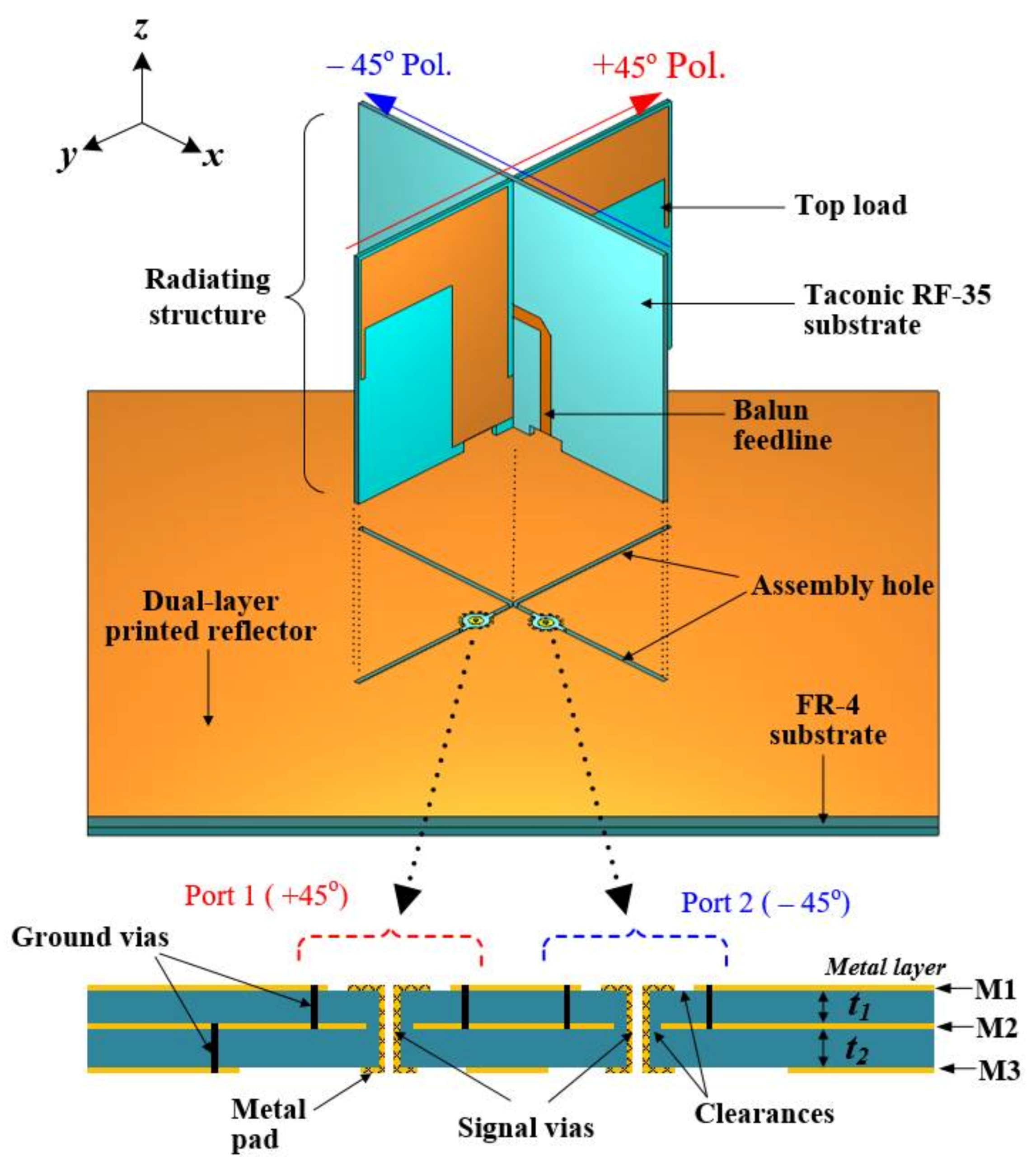
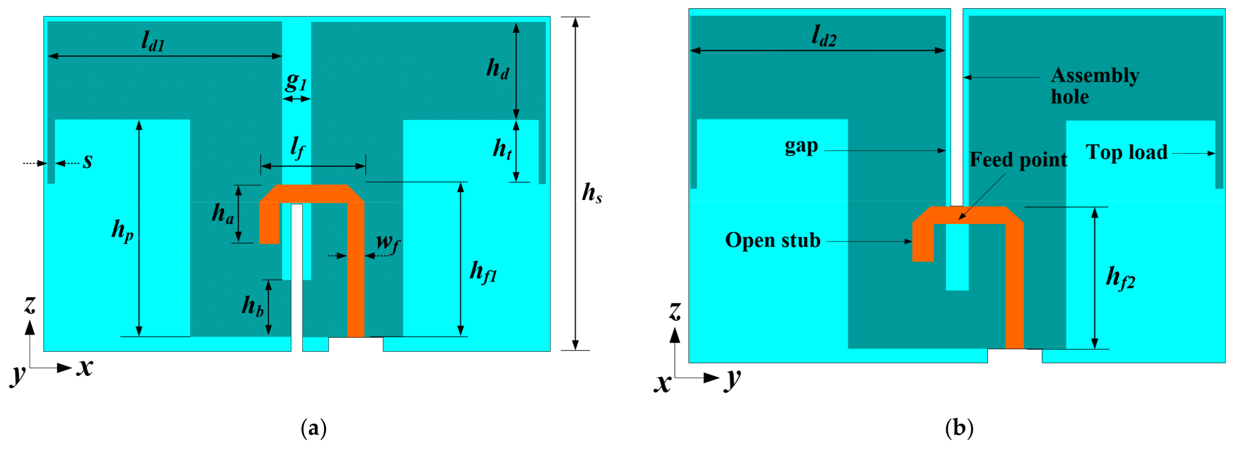
2. Antenna Design
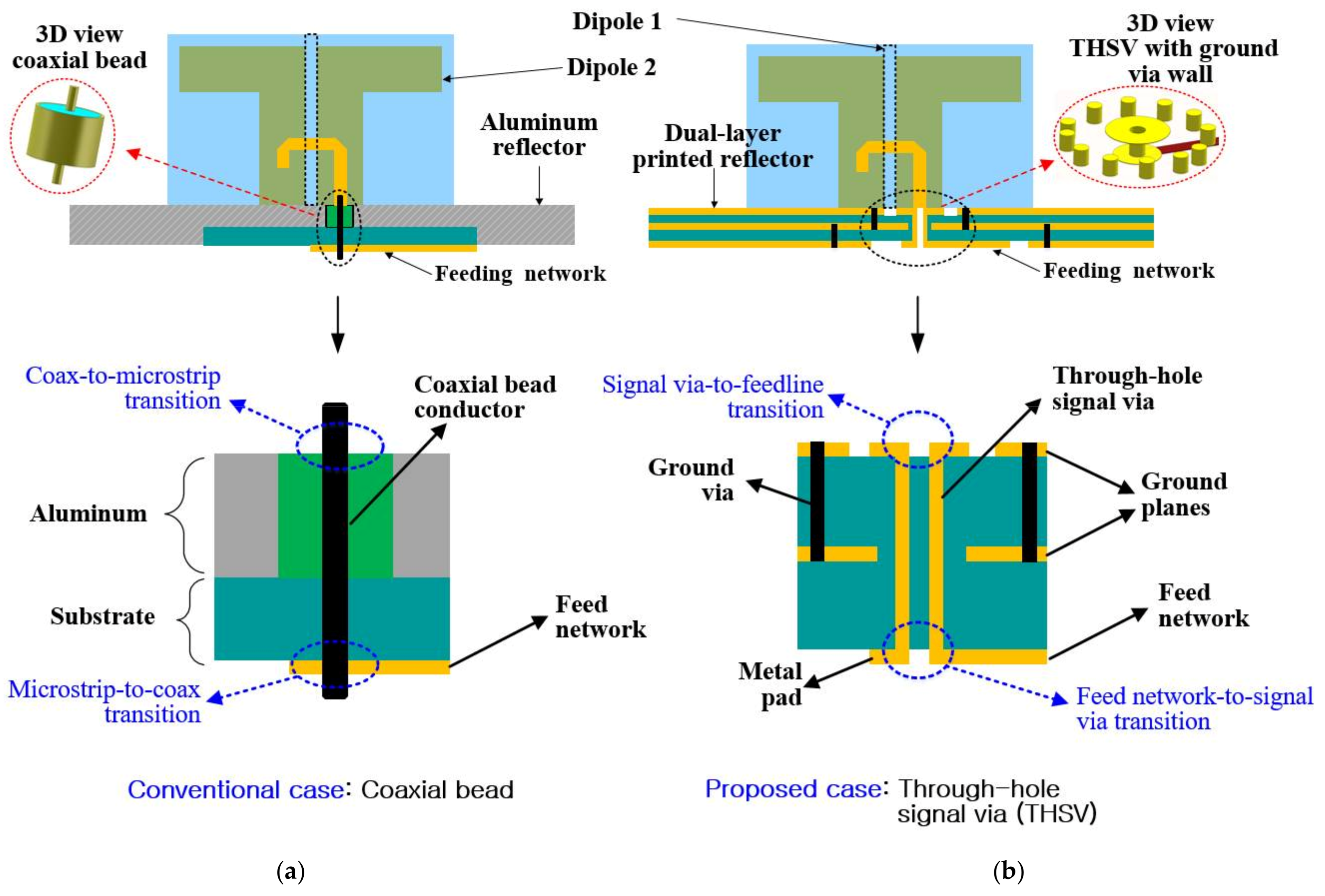
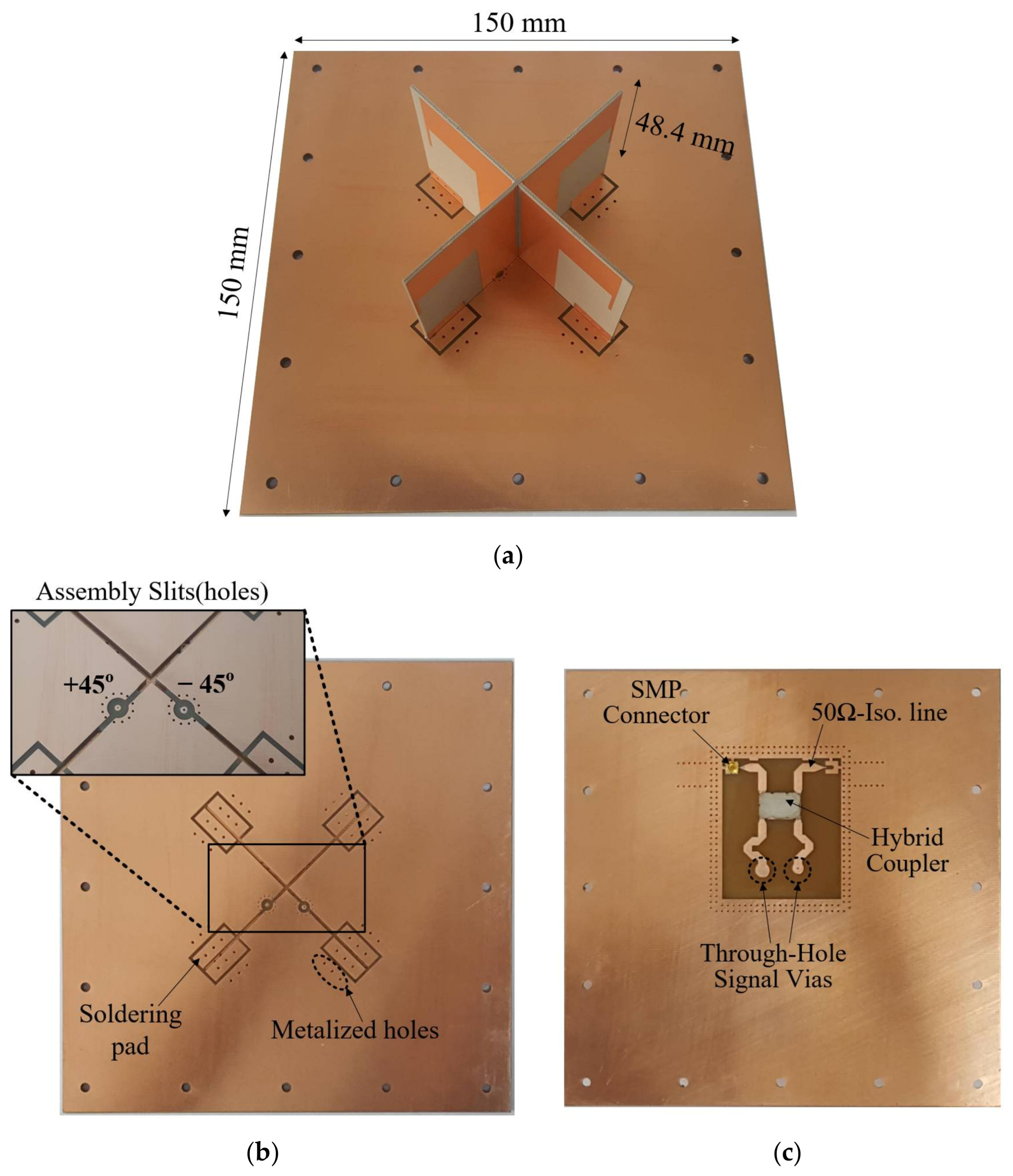
2.1. Feeding Structure Based on Coaxial Bead Conductor
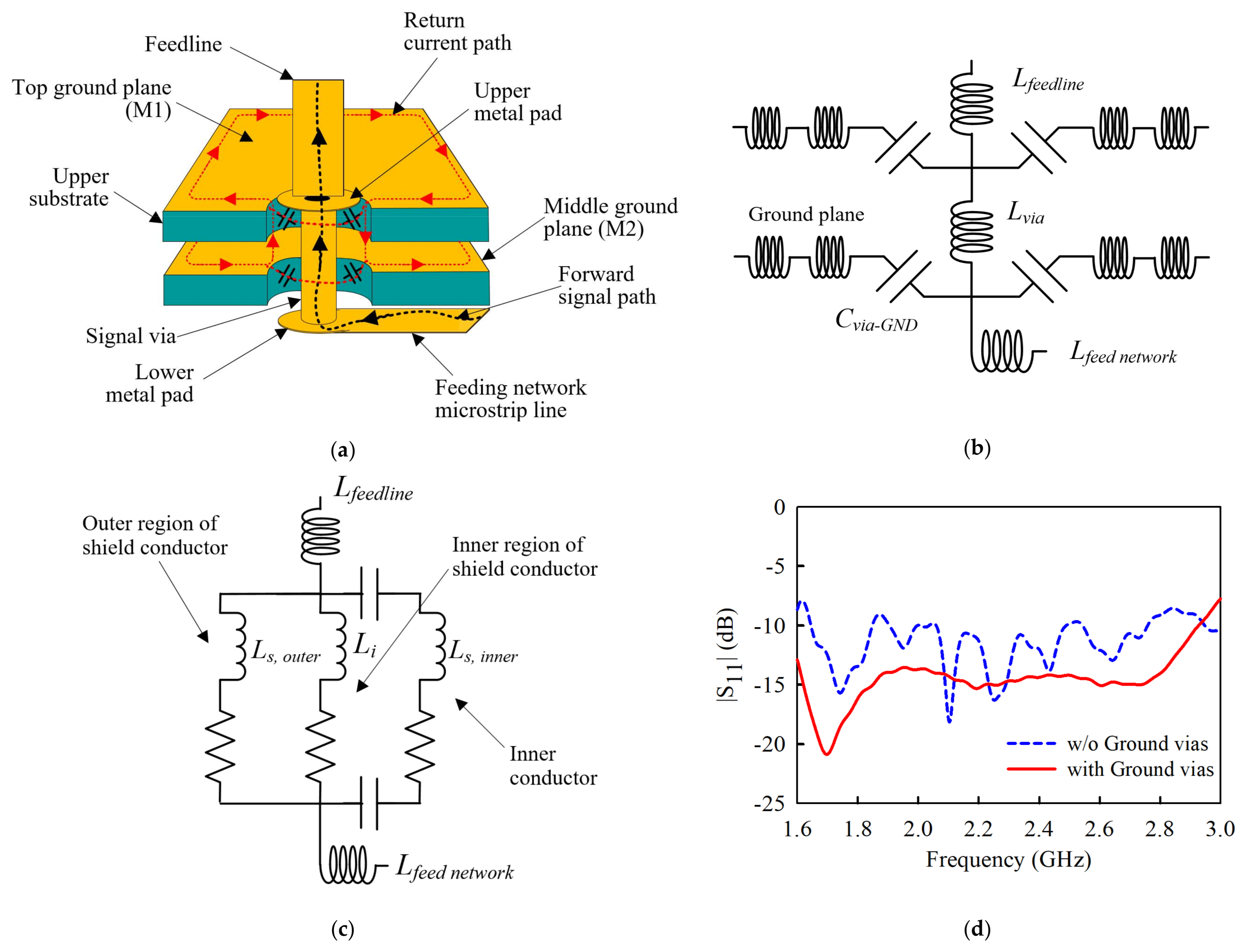
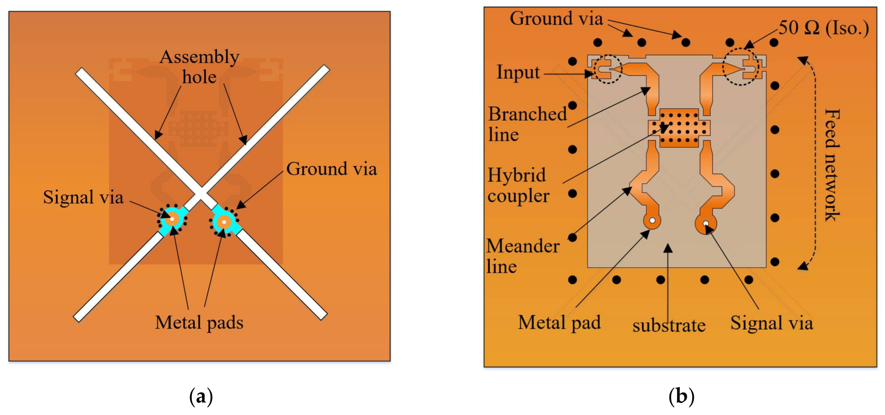
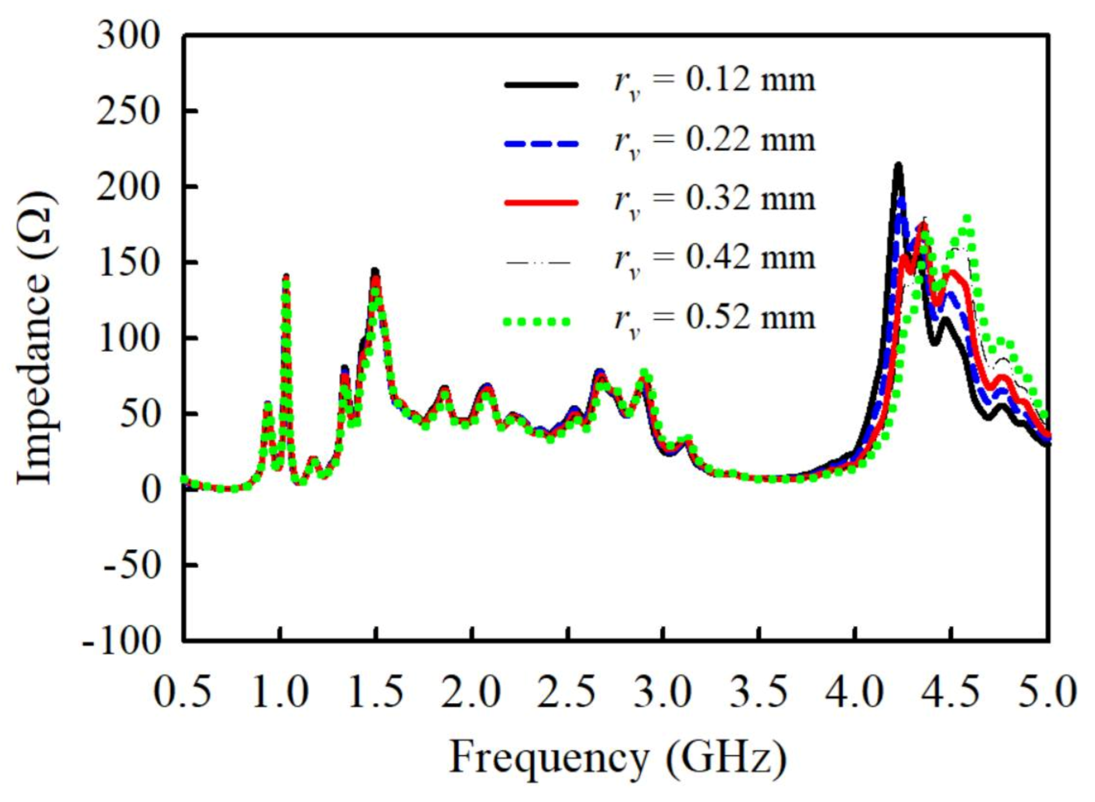
2.2. Proposed Through-Hole Signal via (THSV) Design
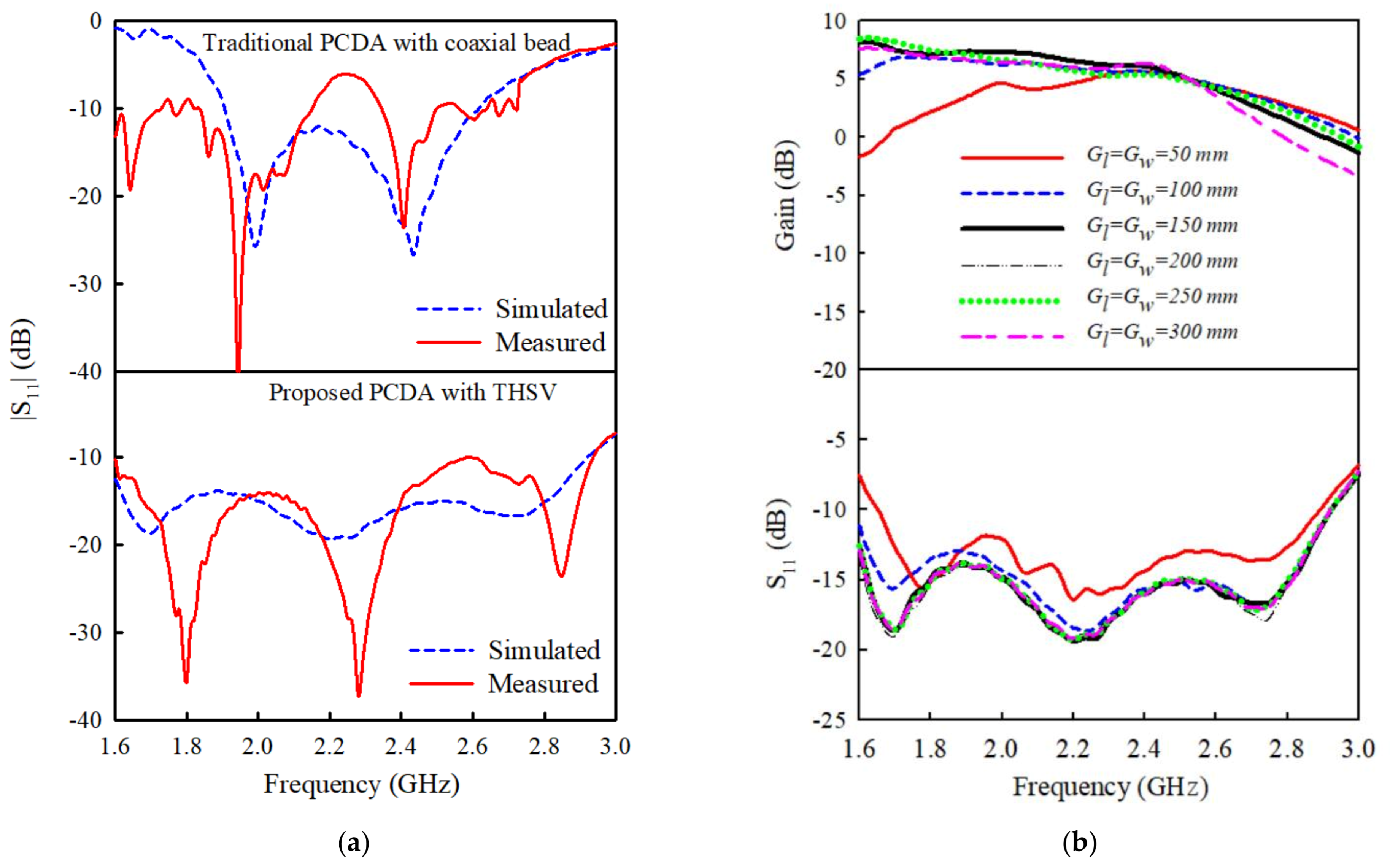
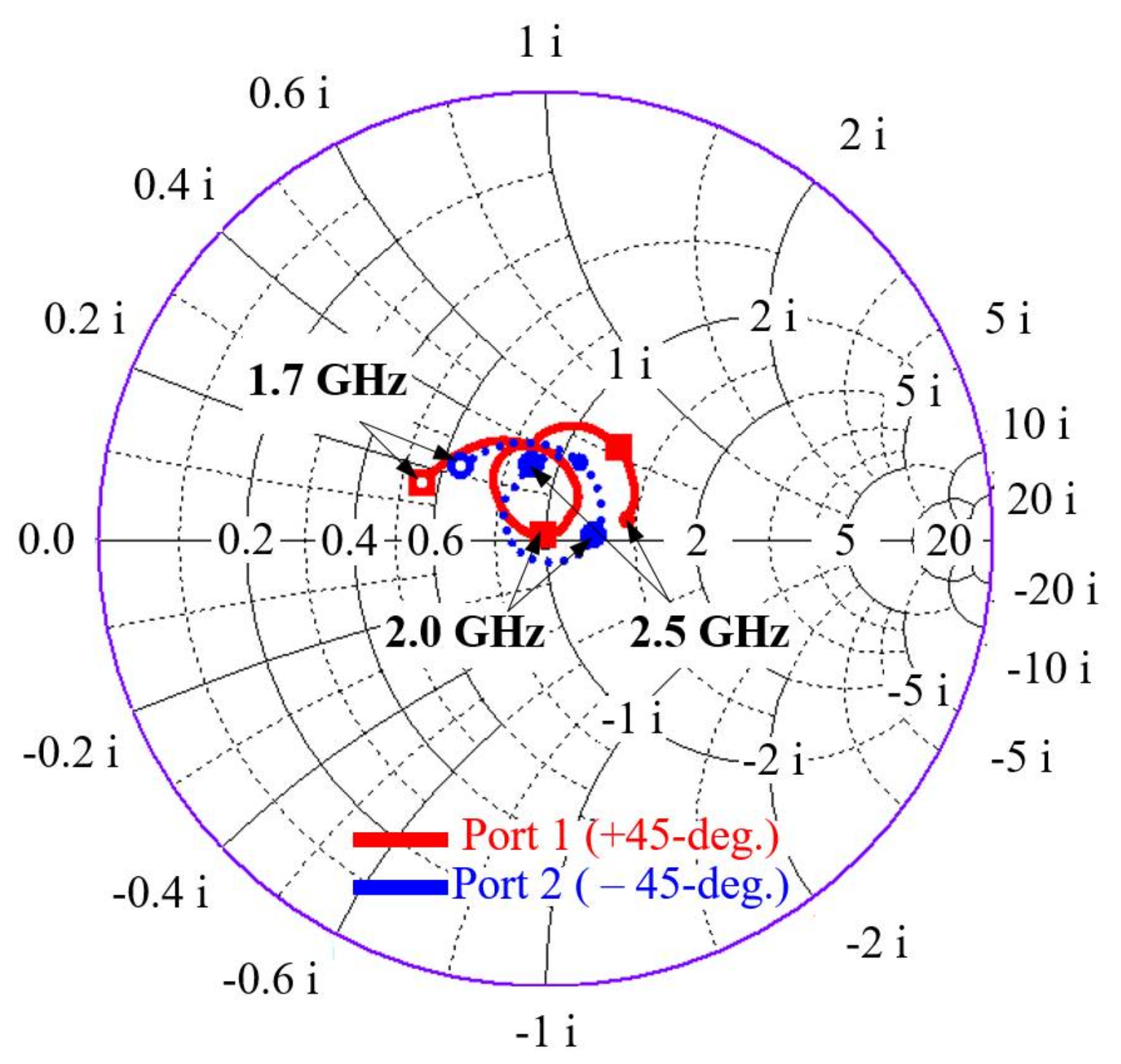
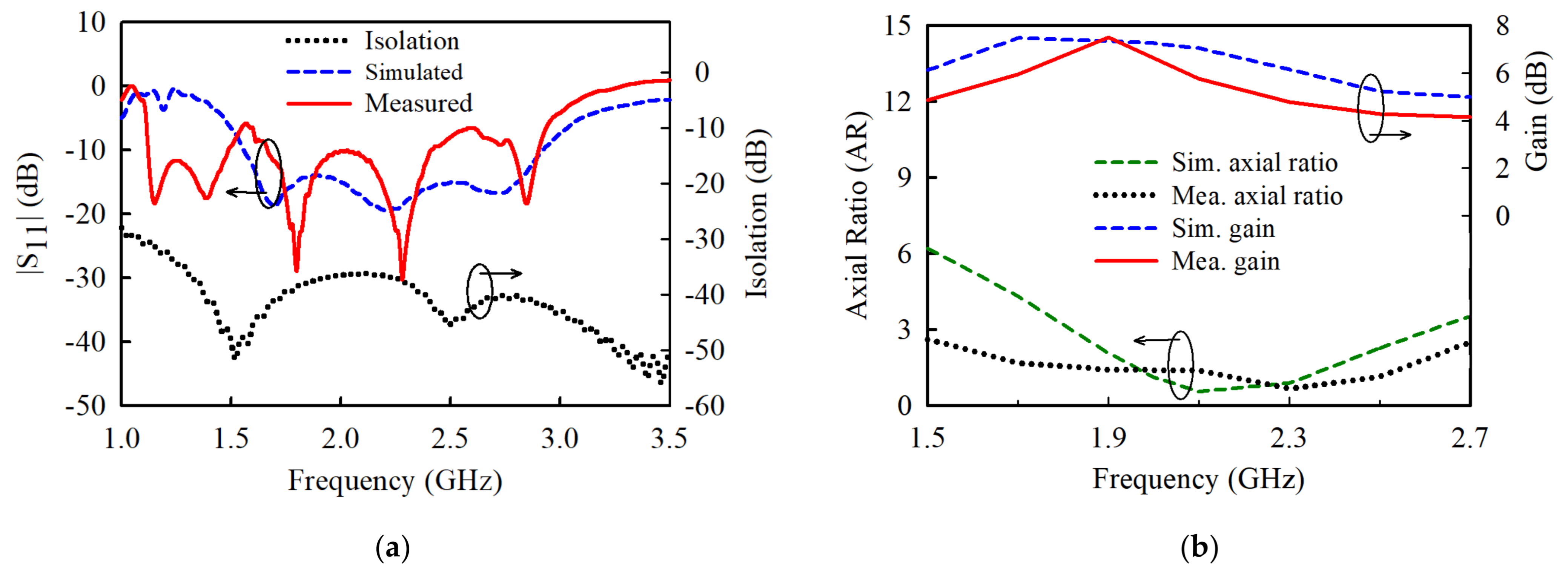
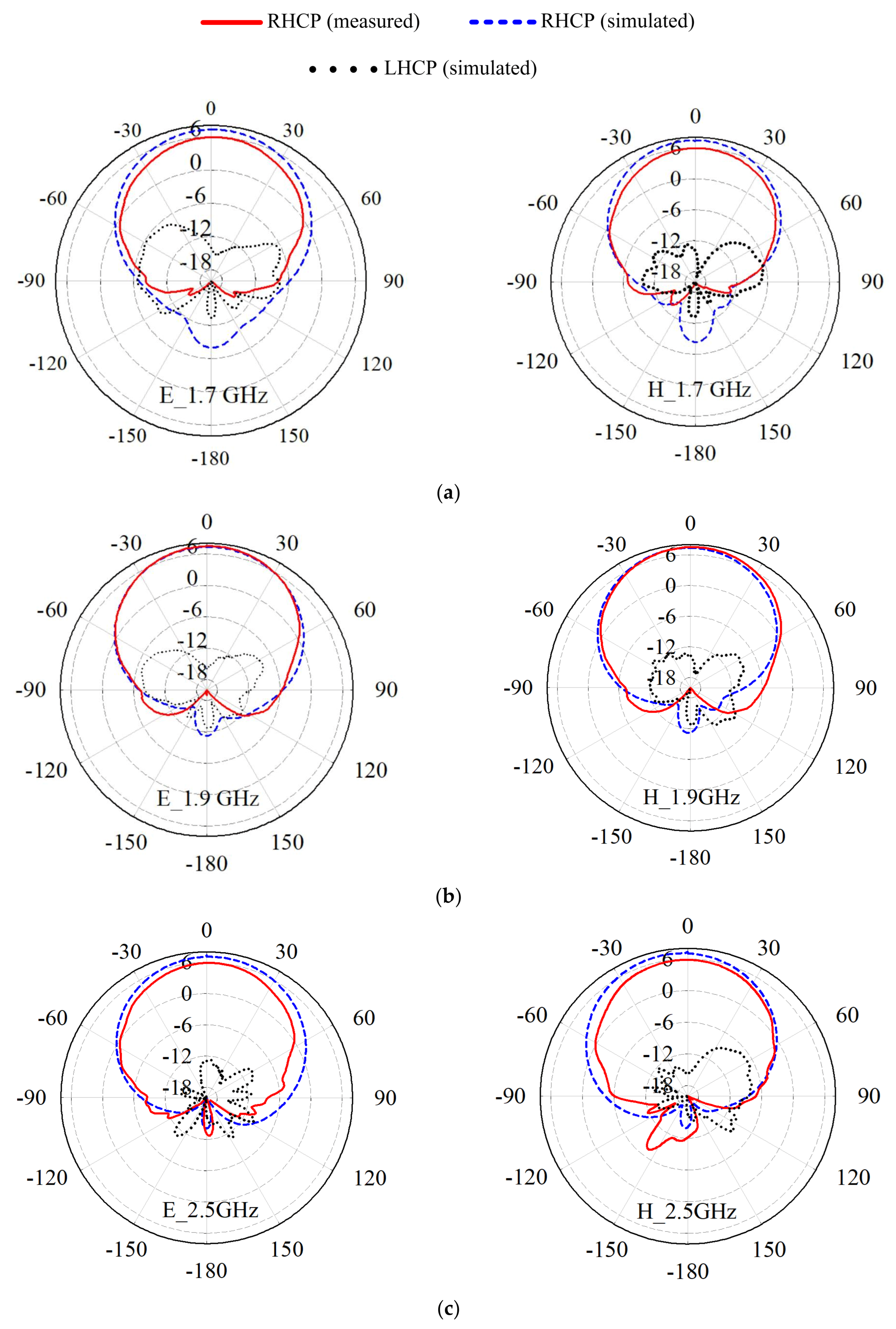
3. Results and Discussions
4. Conclusions
Author Contributions
Funding
Institutional Review Board Statement
Informed Consent Statement
Data Availability Statement
Acknowledgments
Conflicts of Interest
References
- Sun, Y.X.; Leung, K.W.; Lu, K. Broadbeam Cross-Dipole Antenna for GPS Applications. IEEE Trans. Antennas Propag. 2017, 65, 5605–5610. [Google Scholar] [CrossRef]
- Zhang, J.; Yang, H.; Yang, D. Design of a New High-Gain Circularly Polarized Antenna for Inmarsat Communications. IEEE Antennas Wirel. Propag. Lett. 2012, 11, 350–353. [Google Scholar] [CrossRef]
- Mak, K.M.; Luk, K.M. A Circularly Polarized Antenna with Wide Axial Ratio Beamwidth. IEEE Trans. Antennas Propag. 2009, 57, 3309–3312. [Google Scholar]
- Baik, J.; Lee, T.; Pyo, S.; Han, S.M.; Jeong, J.; Kim, Y.S. Broadband Circularly Polarized Crossed Dipole With Parasitic Loop Resonators and Its Arrays. IEEE Trans. Antennas Propag. 2011, 59, 80–88. [Google Scholar] [CrossRef]
- Ta, S.X.; Park, I. Dual-Band Low-Profile Crossed Asymmetric Dipole Antenna on Dual-Band AMC Surface. IEEE Antennas Wirel. Propag. Lett. 2014, 13, 587–590. [Google Scholar]
- Wang, L.; Yang, H.; Li, Y. Design of a New Printed Dipole Antenna Using in High Latitudes for Inmarsat. IEEE Antennas Wirel. Propag. Lett. 2011, 10, 358–360. [Google Scholar] [CrossRef]
- Shi, J.; Yang, S.; Zhai, H.; Li, H. Design of a Printed Broadband Cross-Dipole Antenna. In Proceedings of the 2019 International Symposium on Antennas and Propagation (ISAP), Xi’an, China, 27–30 October 2019; pp. 1–3. [Google Scholar]
- He, Y.; He, W.; Wong, H. A Wideband Circularly Polarized Cross-Dipole Antenna. IEEE Antennas Wirel. Propag. Lett. 2014, 13, 67–70. [Google Scholar]
- Wang, L.; Fang, W.; En, Y.; Huang, Y.; Shao, W.H.; Yao, B. Wideband Circularly Polarized Cross-Dipole Antenna with Parasitic Elements. IEEE Access 2019, 7, 35097–35102. [Google Scholar] [CrossRef]
- Feng, C.; Zhang, F.; Sun, F. A Broadband Crossed Dipole Antenna with Wide Axial Ratio Beamwidth for Satellite Communications. Prog. Electromagn. Res. Lett. 2018, 77, 59–64. [Google Scholar] [CrossRef] [Green Version]
- Cui, Y.H.; Zhang, P.P.; Li, R.L. Broadband quad-polarisation reconfigurable antenna. IET Electron. Lett. 2018, 54, 1199–1200. [Google Scholar] [CrossRef]
- Chen, Y.Y.; Ge, Y.; Li, G. A broadband dual-polarized planar printed dipole fed by a vertical printed balun. In Proceedings of the 2015 IEEE International Wireless Symposium (IWS 2015), Shenzhen, China, 30 March–1 April 2015; pp. 1–3. [Google Scholar]
- Cai, X.; Sarabandi, K. Broadband Omnidirectional Circularly Polarized Antenna with Asymmetric Power Divider. IEEE Trans. Antennas Propag. 2020, 68, 5171–5181. [Google Scholar] [CrossRef]
- Li, R.; Wu, T.; Pan, B.; Lim, K.; Laskar, J.; Tentzeris, M.M. Equivalent-Circuit Analysis of a Broadband Printed Dipole with Adjusted Integrated Balun and an Array for Base Station Applications. IEEE Trans. Antennas Propag. 2009, 57, 2180–2184. [Google Scholar]
- Qu, S.-W.; Chan, C.H.; Xue, Q. Wideband and high-gain composite cavity-backed crossed triangular bowtie dipoles for circular polarized radiation. IEEE Trans. Antennas Propag. 2010, 58, 3157–3164. [Google Scholar] [CrossRef]
- Bao, Z.; Nie, Z.; Zong, X. A novel broadband dual-polarization antenna utilizing strong mutual coupling. IEEE Trans. Antennas Propag. 2014, 62, 450–454. [Google Scholar] [CrossRef]
- Mak, K.; Wong, H.; Luk, K. A Shorted Bowtie Patch Antenna with a Cross Dipole for Dual Polarization. IEEE Antennas Wirel. Propag. Lett. 2007, 6, 126–129. [Google Scholar] [CrossRef]


| Antenna | f (GHz) | IBW (%) | ARBW (%) | Beamwidth (°) | Max. gain (dB) | Size (L × W × H) |
|---|---|---|---|---|---|---|
| Proposed | 2.0 | 59.3 | 57.1 | 65.9–78.3 | 7.5 | 1λ × 1λ × 0.32λ |
| [2] | 1.68 | 38.16 | 12.9 | >60 | 8 | H = 0.37λ (Aperture diameter = 1.086λ) |
| [6] | 1.67 | 40 | 12.9 | 100–110 | 9 | H = 0.456λ (Aperture diameter = 0.52λ) |
| [10] | 2.89 | 70.6 | 62.4 | 94–95 | 6 | 0.674λ × 0.674λ × 0.37λ |
| [11] | 0.84 | 79 | 36 | - | 8 | 0.98λ × 0.98λ × 0.33λ |
| [13] | 1.57 | 66.7 | 57.7 | - | 0.9 | 0.52λ × 0.52λ × 0.65λ |
| [15] | 2.04 | 57 | 39 | - | 10.7 | H = 0.257λ (Aperture diameter = 1.028λ) |
| [16] | 2.33 | 57.5 | Dual Pol. | 58.1–72.6 (E) 76.8–85.5 (H) | 8.8 | 2.33λ × 1.126λ × 0.29λ |
| [17] | 1.94 | 23.7 | Dual Pol. | 76.8–85.5 | 6.9 | 0.97λ × 0.97λ × 0.226λ |
Publisher’s Note: MDPI stays neutral with regard to jurisdictional claims in published maps and institutional affiliations. |
© 2021 by the authors. Licensee MDPI, Basel, Switzerland. This article is an open access article distributed under the terms and conditions of the Creative Commons Attribution (CC BY) license (https://creativecommons.org/licenses/by/4.0/).
Share and Cite
Anim, K.; Park, B.; Lee, H.D.; Jang, S.; Kong, S.; Jung, Y.-B. A Simple Printed Cross-Dipole Antenna with Modified Feeding Structure and Dual-Layer Printed Reflector for Direction Finding Systems. Sensors 2021, 21, 5966. https://doi.org/10.3390/s21175966
Anim K, Park B, Lee HD, Jang S, Kong S, Jung Y-B. A Simple Printed Cross-Dipole Antenna with Modified Feeding Structure and Dual-Layer Printed Reflector for Direction Finding Systems. Sensors. 2021; 21(17):5966. https://doi.org/10.3390/s21175966
Chicago/Turabian StyleAnim, Kyei, Bonghyuk Park, Hui Dong Lee, Seunghyun Jang, Sunwoo Kong, and Young-Bae Jung. 2021. "A Simple Printed Cross-Dipole Antenna with Modified Feeding Structure and Dual-Layer Printed Reflector for Direction Finding Systems" Sensors 21, no. 17: 5966. https://doi.org/10.3390/s21175966
APA StyleAnim, K., Park, B., Lee, H. D., Jang, S., Kong, S., & Jung, Y.-B. (2021). A Simple Printed Cross-Dipole Antenna with Modified Feeding Structure and Dual-Layer Printed Reflector for Direction Finding Systems. Sensors, 21(17), 5966. https://doi.org/10.3390/s21175966