Switched-Biasing Techniques for CMOS Voltage-Controlled Oscillator


Abstract
1. Introduction
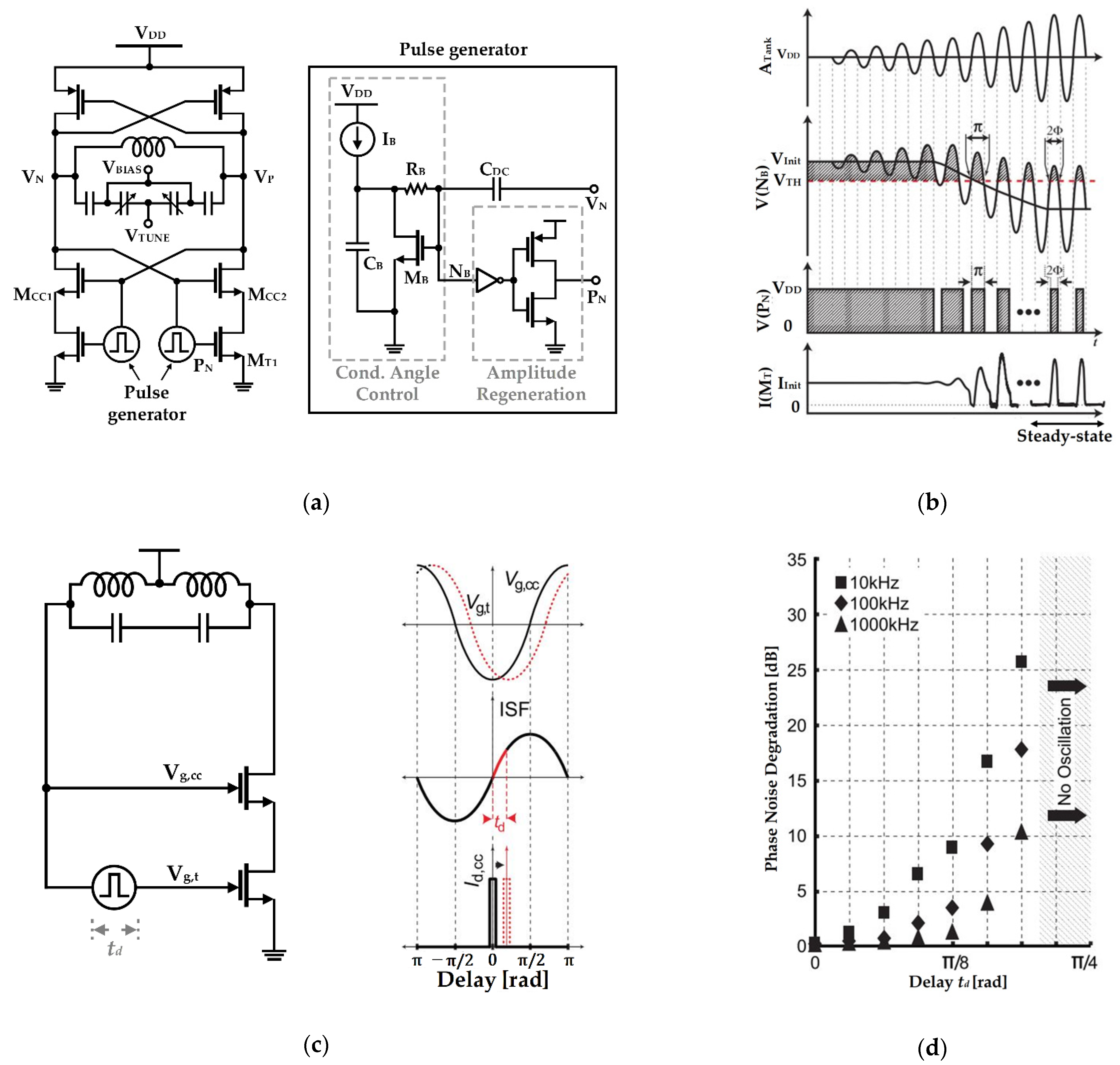
2. Switched-Biasing Technique
3. Circuit Implementation
- Modulation frequency and amplitude
- Modulation waveform
- DC bias voltage
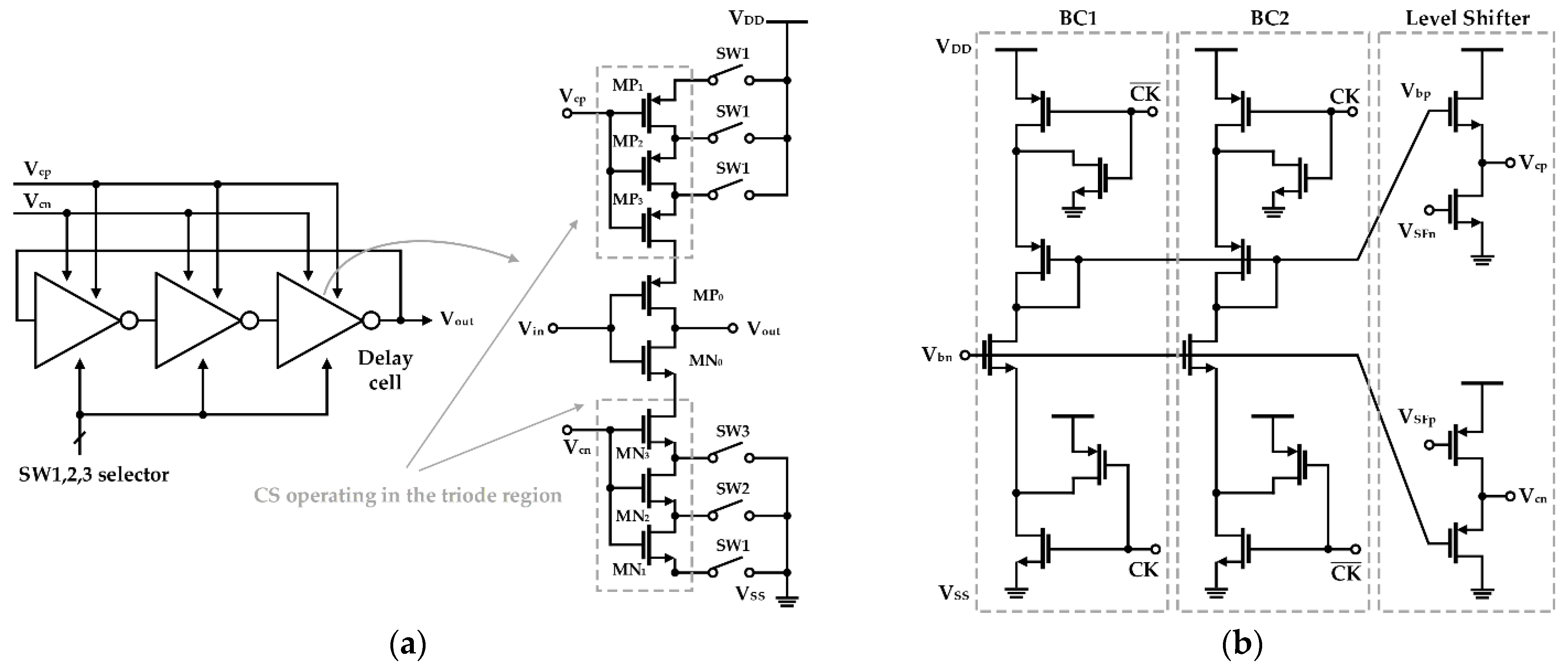
3.1. External-Biasing Topology
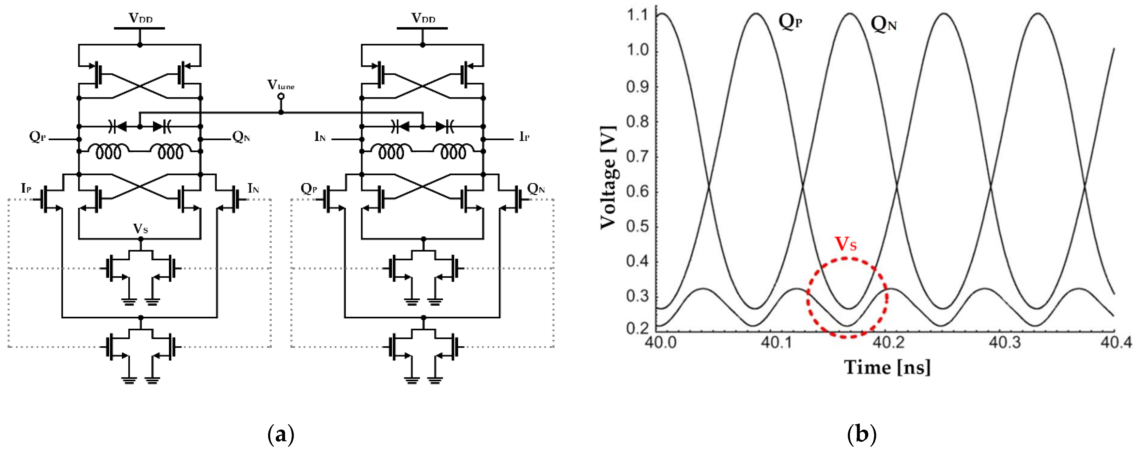
3.2. Self-Biasing Topology with the Fixed DC Voltage
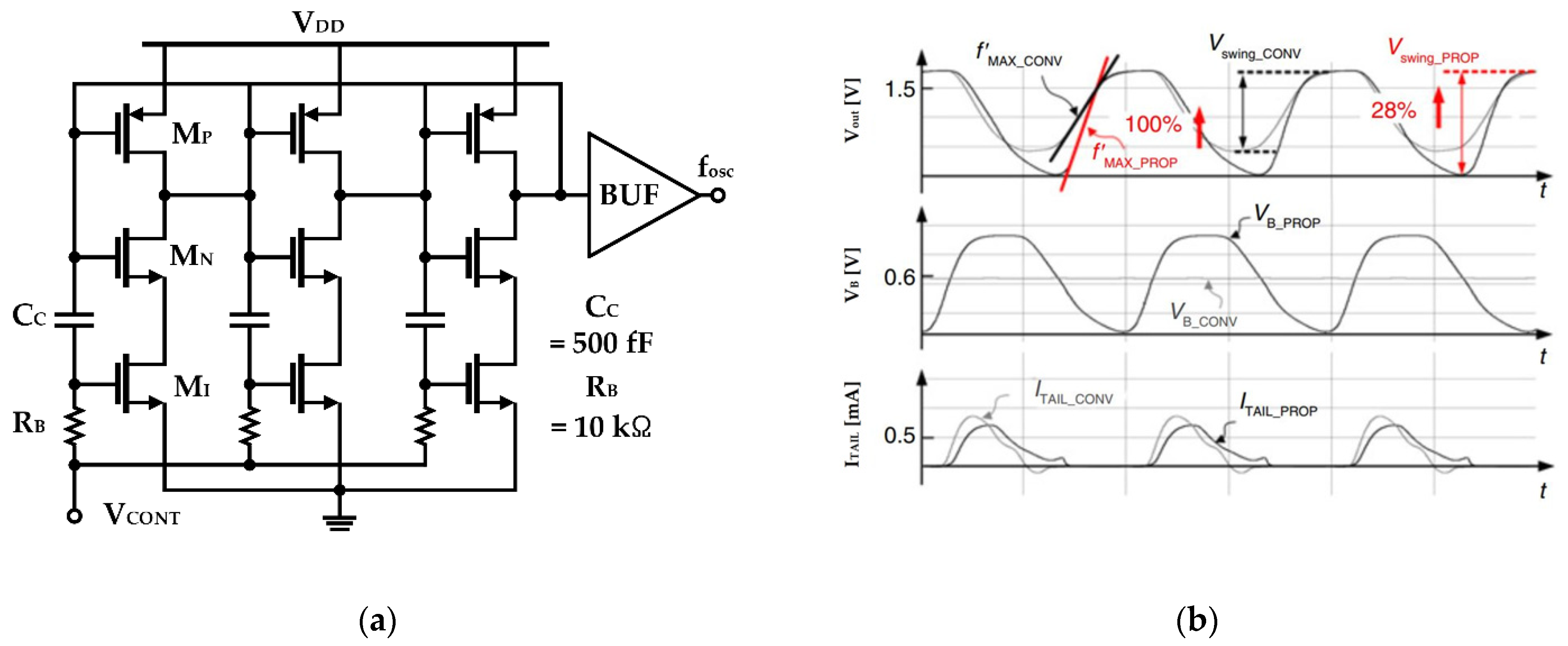
3.3. Self-Biased Topology with the Adaptive DC Voltage
4. Discussion
5. Conclusions
Author Contributions
Funding
Institutional Review Board Statement
Informed Consent Statement
Data Availability Statement
Acknowledgments
Conflicts of Interest
References
- Jann, B.; Chance, G.; Roy, A.G.; Balakrishnan, A.; Karandikar, N.; Brown, T.; Li, X.; Davis, B.; Ceballos, J.L.; Tanzi, N.; et al. 21.5 A 5G Sub-6GHz Zero-IF and mm-Wave IF Transceiver with MIMO and Carrier Aggregation. In Proceedings of the 2019 IEEE International Solid- State Circuits Conference—(ISSCC), San Francisco, CA, USA, 17–21 February 2019; pp. 352–354. [Google Scholar]
- Khalaf, K.; Vaesen, K.; Brebels, S.; Mangraviti, G.; Libois, M.; Soens, C.; Thillo, W.V.; Wambacq, P. A 60-GHz 8-Way Phased-Array Front-End With T/R Switching and Calibration-Free Beamsteering in 28-nm CMOS. IEEE J. Solid-State Circuits 2018, 53, 2001–2011. [Google Scholar] [CrossRef]
- Dunworth, J.D.; Homayoun, A.; Ku, B.; Ou, Y.; Chakraborty, K.; Liu, G.; Segoria, T.; Lerdworatawee, J.; Park, J.W.; Park, H.; et al. A 28GHz Bulk-CMOS Dual-Polarization Phased-Array Transceiver with 24 Channels for 5G User and Basestation Equipment. In Proceedings of the 2018 IEEE International Solid—State Circuits Conference—(ISSCC), San Francisco, CA, USA, 11–15 February 2018; pp. 70–72. [Google Scholar]
- Angevare, J.; Pedalà, L.; Sönmez, U.; Sebastiano, F.; Makinwa, K.A.A. A 2800-μm2 Thermal-Diffusivity Temperature Sensor with VCO-Based Readout in 160-nm CMOS. In Proceedings of the 2015 IEEE Asian Solid-State Circuits Conference (A-SSCC), Xiamen, China, 9–11 November 2015; pp. 1–4. [Google Scholar]
- Enache, A.; Drăghici, F.; Pristavu, G.; Brezeanu, G. Voltage Controlled Oscillator for Small-Signal Capacitance Sensing. In Proceedings of the 2019 International Semiconductor Conference (CAS), Sinaia, Romania, 9–11 October 2019; pp. 323–326. [Google Scholar]
- Quintero, A.; Cardes, F.; Perez, C.; Buffa, C.; Wiesbauer, A.; Hernandez, L. A VCO-Based CMOS Readout Circuit for Capacitive MEMS Microphones. Sensors 2019, 19, 4126. [Google Scholar] [CrossRef] [PubMed]
- Vornicu, I.; Carmona-Galán, R.; Rodríguez-Vázquez, Á. Arrayable Voltage-Controlled Ring-Oscillator for Direct Time-of-Flight Image Sensors. IEEE Trans. Circuits Syst. Regul. Pap. 2017, 64, 2821–2834. [Google Scholar] [CrossRef]
- Tseng, S.; Kao, Y.; Peng, C.; Liu, J.; Chu, S.; Hong, G.; Hsieh, C.; Hsu, K.; Liu, W.; Huang, Y.; et al. A 65-nm CMOS Low-Power Impulse Radar System for Human Respiratory Feature Extraction and Diagnosis on Respiratory Diseases. IEEE Trans. Microw. Theory Tech. 2016, 64, 1029–1041. [Google Scholar] [CrossRef]
- Park, J.-H.; Yang, J.-R. Two-Tone Continuous-Wave Doppler Radar Based on Envelope Detection Method. Microw. Opt. Technol. Lett. 2020, 62, 3146–3150. [Google Scholar] [CrossRef]
- Sim, J.Y.; Park, J.-H.; Yang, J.-R. Vital-Signs Detector Based on Frequency-Shift Keying Radar. Sensors 2020, 20, 5516. [Google Scholar] [CrossRef] [PubMed]
- Bassi, M.; Caruso, M.; Bevilacqua, A.; Neviani, A. A 65-nm CMOS 1.75–15 GHz Stepped Frequency Radar Receiver for Early Diagnosis of Breast Cancer. IEEE J. Solid-State Circuits 2013, 48, 1741–1750. [Google Scholar] [CrossRef]
- Tu, C.; Wang, Y.; Lin, T. A Low-Noise Area-Efficient Chopped VCO-Based CTDSM for Sensor Applications in 40-nm CMOS. IEEE J. Solid-State Circuits 2017, 52, 2523–2532. [Google Scholar] [CrossRef]
- Peng, K.; Chen, S.; Wang, F.; Horng, T. Enhancement of Vital-Sign Sensor Signal-to-Noise Ratio Using Wireless Frequency-Locked Loop. In Proceedings of the 2019 IEEE SENSORS, Montreal, QC, Canada, 27−30 October 2019; pp. 1–3. [Google Scholar]
- Pepe, F.; Bonfanti, A.; Levantino, S.; Samori, C.; Lacaita, A.L. Analysis and Minimization of Flicker Noise Up-Conversion in Voltage-Biased Oscillators. IEEE Trans. Microw. Theory Tech. 2013, 61, 2382–2394. [Google Scholar] [CrossRef]
- Hu, Y.; Siriburanon, T.; Staszewski, R.B. A Low-Flicker-Noise 30-GHz Class-F23 Oscillator in 28-nm CMOS Using Implicit Resonance and Explicit Common-Mode Return Path. IEEE J. Solid-State Circuits 2018, 53, 1977–1987. [Google Scholar] [CrossRef]
- Tang, K.; Lou, L.; Guo, T.; Chen, B.; Wang, Y.; Fang, Z.; Yang, C.; Wang, W.; Zheng, Y. A 4TX/4RX Pulsed Chirping Phased-Array Radar Transceiver in 65-nm CMOS for X-Band Synthetic Aperture Radar Application. IEEE J. Solid-State Circuits 2020, 55, 2970–2983. [Google Scholar] [CrossRef]
- Bennett, H.; Brederlow, R.; Costa, J.; Cottrell, P.; Huang, W.; Immorlica, A.; Mueller, J.-E.; Racanelli, M.; Shichijo, H.; Weitzel, C.; et al. Device and Technology Evolution for Si-Based RF Integrated Circuits. IEEE Trans. Electron Devices 2005, 52, 1235–1258. [Google Scholar] [CrossRef]
- Razavi, B. RF Microelectronics (2nd Edition) (Prentice Hall Communications Engineering and Emerging Technologies Series), 2nd ed.; Prentice Hall Press: Upper Saddle River, NJ, USA, 2011; ISBN 978-0-13-713473-1. [Google Scholar]
- Nemirovsky, Y.; Corcos, D.; Brouk, I.; Nemirovsky, A.; Chaudhry, S. 1/f Noise in Advanced CMOS Transistors. IEEE Instrum. Meas. Mag. 2011, 14, 14–22. [Google Scholar] [CrossRef]
- Leeson, D.B. A Simple Model of Feedback Oscillator Noise Spectrum. Proc. IEEE 1966, 54, 329–330. [Google Scholar] [CrossRef]
- Bevilacqua, A.; Andreani, P. An Analysis of 1/f Noise to Phase Noise Conversion in CMOS Harmonic Oscillators. IEEE Trans. Circuits Syst. Regul. Pap. 2012, 59, 938–945. [Google Scholar] [CrossRef]
- Hu, Y.; Siriburanon, T.; Staszewski, R.B. Intuitive Understanding of Flicker Noise Reduction via Narrowing of Conduction Angle in Voltage-Biased Oscillators. IEEE Trans. Circuits Syst. II Express Briefs 2019, 66, 1962–1966. [Google Scholar] [CrossRef]
- Franceschin, A.; Andreani, P.; Padovan, F.; Bassi, M.; Bevilacqua, A. A 19.5-GHz 28-nm Class-C CMOS VCO, with a Reasonably Rigorous Result on 1/f Noise Upconversion Caused by Short-Channel Effects. IEEE J. Solid-State Circuits 2020, 55, 1842–1853. [Google Scholar] [CrossRef]
- Mazzanti, A.; Andreani, P. Class-C Harmonic CMOS VCOs, With a General Result on Phase Noise. IEEE J. Solid-State Circuits 2008, 43, 2716–2729. [Google Scholar] [CrossRef]
- Deng, W.; Okada, K.; Matsuzawa, A. Class-C VCO With Amplitude Feedback Loop for Robust Start-Up and Enhanced Oscillation Swing. IEEE J. Solid-State Circuits 2013, 48, 429–440. [Google Scholar] [CrossRef]
- Hong, C.-H.; Wu, C.-Y.; Liao, Y.-T. Robustness Enhancement of a Class-C Quadrature Oscillator Using Capacitive Source Degeneration Coupling. IEEE Trans. Circuits Syst. II Express Briefs 2015, 62, 16–20. [Google Scholar] [CrossRef]
- Hegazi, E.; Sjoland, H.; Abidi, A.A. A Filtering Technique to Lower LC Oscillator Phase Noise. IEEE J. Solid-State Circuits 2001, 36, 1921–1930. [Google Scholar] [CrossRef]
- Murphy, D.; Darabi, H. 2.5 A Complementary VCO for IoE That Achieves a 195 dBc/Hz FOM and Flicker Noise Corner of 200 kHz. In Proceedings of the 2016 IEEE International Solid-State Circuits Conference (ISSCC), San Francisco, CA, USA, 31 January−4 February 2016; pp. 44–45. [Google Scholar]
- Guo, H.; Chen, Y.; Mak, P.; Martins, R.P. 26.2 A 0.08 mm2 25.5-to −29.9 GHz Multi-Resonant-RLCM-Tank VCO Using a Single-Turn Multi-Tap Inductor and CM-Only Capacitors Achieving 191.6 dBc/Hz FoM and 130 kHz 1/f3 PN Corner. In Proceedings of the 2019 IEEE International Solid- State Circuits Conference—(ISSCC), San Francisco, CA, USA, 17−21 February 2019; pp. 410–412. [Google Scholar]
- Rael, J.J.; Abidi, A.A. Physical Processes of Phase Noise in Differential LC Oscillators. In Proceedings of the IEEE 2000 Custom Integrated Circuits Conference (Cat. No. 00CH37044), Orlando, FL, USA, 24 May 2000; pp. 569–572. [Google Scholar]
- Shahmohammadi, M.; Babaie, M.; Staszewski, R.B. A 1/f Noise Upconversion Reduction Technique for Voltage-Biased RF CMOS Oscillators. IEEE J. Solid-State Circuits 2016, 51, 2610–2624. [Google Scholar] [CrossRef]
- Gierkink, S.L.J.; Klumperink, E.A.M.; van der Wel, A.P.; Hoogzaad, G.; van Tuijl, E.A.J.M.; Nauta, B. Intrinsic 1/f Device Noise Reduction and Its Effect on Phase Noise in CMOS Ring Oscillators. IEEE J. Solid-State Circuits 1999, 34, 1022–1025. [Google Scholar] [CrossRef]
- Klumperink, E.A.M.; Gierkink, S.L.J.; van der Wel, A.P.; Nauta, B. Reducing MOSFET 1/f Noise and Power Consumption by Switched Biasing. IEEE J. Solid-State Circuits 2000, 35, 994–1001. [Google Scholar] [CrossRef]
- Boon, C.C.; Do, M.A.; Yeo, K.S.; Ma, J.G.; Zhang, X.L. RF CMOS Low-Phase-Noise LC Oscillator through Memory Reduction Tail Transistor. IEEE Trans. Circuits Syst. II Express Briefs 2004, 51, 85–90. [Google Scholar] [CrossRef]
- Hooge, F.N. 1/f Noise. Phys. BC 1976, 83, 14–23. [Google Scholar] [CrossRef]
- Keshner, M.S. 1/f Noise. Proc. IEEE 1982, 70, 212–218. [Google Scholar] [CrossRef]
- Hooge, F.N. 1/ƒ Noise Is No Surface Effect. Phys. Lett. A 1969, 29, 139–140. [Google Scholar] [CrossRef]
- McWhorter, A.L. 1/f Noise and Related Surface Effects in Germanium. Ph.D. Thesis, Massachusetts Institute of Technology, Cambridge, MA, USA, 1955. [Google Scholar]
- Kirton, M.J.; Uren, M.J. Noise in Solid-State Microstructures: A New Perspective on Individual Defects, Interface States and Low-Frequency (1/ƒ) Noise. Adv. Phys. 1989, 38, 367–468. [Google Scholar] [CrossRef]
- Bloom, I.; Nemirovsky, Y. 1/ f Noise Reduction of Metal-oxide-semiconductor Transistors by Cycling from Inversion to Accumulation. Appl. Phys. Lett. 1991, 58, 1664–1666. [Google Scholar] [CrossRef]
- Dierickx, B.; Simoen, E. The Decrease of ‘“Random Telegraph Signal”’ Noise in Metal-oxide-semiconductor Field-effect Transistors When Cycled from Inversion to Accumulation. J. Appl. Phys. 1992, 71, 2028–2029. [Google Scholar] [CrossRef]
- van der Wel, A.P.; Klumperink, E.A.M.; Gierkink, S.L.J.; Wassenaar, R.F.; Wallinga, H. MOSFET 1/f Noise Measurement under Switched Bias Conditions. IEEE Electron Device Lett. 2000, 21, 43–46. [Google Scholar] [CrossRef]
- Kolhatkar, J.S.; Salm, C.; Knitel, M.J.; Wallinga, H. Constant and Switched Bias Low Frequency Noise in p-MOSFETs with Varying Gate Oxide Thickness. In Proceedings of the 32nd European Solid-State Device Research Conference, Firenze, Italy, 24−26 September 2002; pp. 83–86. [Google Scholar]
- van der Wel, A.P.; Klumperink, E.A.M.; Kolhatkar, J.S.; Hoekstra, E.; Snoeij, M.F.; Salm, C.; Wallinga, H.; Nauta, B. Low-Frequency Noise Phenomena in Switched MOSFETs. IEEE J. Solid-State Circuits 2007, 42, 540–550. [Google Scholar] [CrossRef]
- Koh, J.; Schmitt-Landsiedel, D.; Thewes, R.; Brederlow, R. A Complementary Switched MOSFET Architecture for the 1/f Noise Reduction in Linear Analog CMOS ICs. IEEE J. Solid-State Circuits 2007, 42, 1352–1361. [Google Scholar] [CrossRef]
- Kim, J.; An, H.; Yun, T. A Low-Noise WLAN Mixer Using Switched Biasing Technique. IEEE Microw. Wirel. Compon. Lett. 2009, 19, 650–652. [Google Scholar] [CrossRef]
- Soltanian, B.; Kinget, P.R. Tail Current-Shaping to Improve Phase Noise in LC Voltage-Controlled Oscillators. IEEE J. Solid-State Circuits 2006, 41, 1792–1802. [Google Scholar] [CrossRef]
- Hajimiri, A.; Lee, T.H. A General Theory of Phase Noise in Electrical Oscillators. IEEE J. Solid-State Circuits 1998, 33, 179–194. [Google Scholar] [CrossRef]
- van der Wel, A.P.; Klumperink, E.A.M.; Nauta, B. Measurement of MOSFET LF Noise under Large Signal RF Excitation. In Proceedings of the 32nd European Solid-State Device Research Conference, Firenze, Italy, 24−26 September 2002; pp. 91–94. [Google Scholar]
- Yoshida, T.; Ishida, N.; Sasaki, M.; Iwata, A. Low-Voltage, Low-Phase-Noise Ring Voltage-Controlled Oscillator Using 1/f-Noise Reduction Techniques. Jpn. J. Appl. Phys. 2007, 46, 2257. [Google Scholar] [CrossRef]
- Musa, A.; Murakami, R.; Sato, T.; Chaivipas, W.; Okada, K.; Matsuzawa, A. A Low Phase Noise Quadrature Injection Locked Frequency Synthesizer for MM-Wave Applications. IEEE J. Solid-State Circuits 2011, 46, 2635–2649. [Google Scholar] [CrossRef]
- Huang, G.; Kim, B. Low Phase Noise Self-Switched Biasing CMOS LC Quadrature VCO. IEEE Trans. Microw. Theory Tech. 2009, 57, 344–351. [Google Scholar] [CrossRef]
- Hsieh, J.; Lin, K. A 0.7-mW LC Voltage-Controlled Oscillator Leveraging Switched Biasing Technique for Low Phase Noise. IEEE Trans. Circuits Syst. II Express Briefs 2019, 66, 1307–1310. [Google Scholar] [CrossRef]
- Shasidharan, P.; Ramiah, H.; Rajendran, J. A 2.2 to 2.9 GHz Complementary Class-C VCO with PMOS Tail-Current Source Feedback Achieving—120 dBc/Hz Phase Noise at 1 MHz Offset. IEEE Access 2019, 7, 91325–91336. [Google Scholar] [CrossRef]
- Hsin-Shu, C.; Ito, A. Hsin-Shu Chen; Ito, A. Characterization of 1/f Noise vs. Number of Gate Stripes in MOS Transistors. In Proceedings of the 1999 IEEE International Symposium on Circuits and Systems (ISCAS), Orlando, FL, USA, 30 May–2 June 1999; Volume 2, pp. 310–313. [Google Scholar]
- Zhang, Z.; Lau, J. Experimental Study on MOSFET’s Flicker Noise under Switching Conditions and Modelling in RF Applications. In Proceedings of the IEEE 2001 Custom Integrated Circuits Conference (Cat. No.01CH37169), San Diego, CA, USA, 9 May 2001; pp. 393–396. [Google Scholar]
- Jeong, C.; Yoo, C. 5-GHz Low-Phase Noise CMOS Quadrature VCO. IEEE Microw. Wirel. Compon. Lett. 2006, 16, 609–611. [Google Scholar] [CrossRef]
- Chen, N.; Diao, S.; Huang, L.; Lin, F. Reduction of 1/f3 Phase Noise in LC Oscillator with Improved Self-Switched Biasing. Analog Integr. Circuits Signal Process. 2015, 84, 19–27. [Google Scholar] [CrossRef]
- Tchamov, N.N.; Tchamov, N.T. Technique for Flicker Noise Up-Conversion Suppression in Differential LC Oscillators. IEEE Trans. Circuits Syst. II Express Briefs 2007, 54, 959–963. [Google Scholar] [CrossRef]
- Mostajeran, A.; Bakhtiar, M.S.; Afshari, E. 25.8 A 2.4GHz VCO with FOM of 190 dBc/Hz at 10 kHz-to −2 MHz Offset Frequencies in 0.13 μm CMOS Using an ISF Manipulation Technique. In Proceedings of the 2015 IEEE International Solid-State Circuits Conference—(ISSCC) Digest of Technical Papers, San Francisco, CA, USA, 22−26 February 2015; pp. 1–3. [Google Scholar]
- Lee, I.; Im, D. Low Phase Noise Ring VCO Employing Input-Coupled Dynamic Current Source. Electron. Lett. 2020, 56, 76–78. [Google Scholar] [CrossRef]
- Hajimiri, A.; Limotyrakis, S.; Lee, T.H. Jitter and Phase Noise in Ring Oscillators. IEEE J. Solid-State Circuits 1999, 34, 790–804. [Google Scholar] [CrossRef]
- Min, B.-H.; Hyun, S.-B.; Yu, H.-K. Low Voltage CMOS LC VCO with Switched Self-Biasing. ETRI J. 2009, 31, 755–764. [Google Scholar] [CrossRef]
- Narayanan, A.T.; Okada, K. A Pulse-Tail-Feedback LC-VCO with 700Hz Flicker Noise Corner and -195dBc FoM. IEICE Trans. Electron. 2019, E102, 595–606. [Google Scholar] [CrossRef]
- Kinget, P. Integrated GHz Voltage Controlled Oscillators. In Analog Circuit Design; Sansen, W., Huijsing, J., van de Plassche, R., Eds.; Springer US: Boston, MA, USA, 1999; pp. 353–381. ISBN 978-1-4419-5101-4. [Google Scholar]


| Topologies | Bias Techniques | Advantages | Disadvantages |
|---|---|---|---|
| External-biasing | - The current source’s gate is biased by external clock generator. | - Effectively reducing flicker noise generation. |
|
| Self-biasing with the fixed DC voltage |
|
|
|
| Self-biasing with the adaptive DC voltage |
|
|
|
| Ref. (year) | Process (µm) | Bias Scheme | VCO Type | VDD (V) | Freq. (GHz) | Tuning Range (%) | Phase Noise @1 MHz (dBc/Hz) | Power (mW) | FoM @1 MHz (dBc/Hz) | FoMT @1 MHz (dBc/Hz) |
|---|---|---|---|---|---|---|---|---|---|---|
| [50] | 0.18 | External biasing | CMOS | 1 | 1 | 82 | −88 1 | 0.71 | −149 1 | −168 1 |
| (2007) | Ring VCO | |||||||||
| [61] | 0.18 | Self-biasing w. fixed DC | CMOS | 1.8 | 1 | 47.6 | −106 | 1.2 | −165 | −179 |
| (2020) | Ring VCO | |||||||||
| [51] | 0.065 | Self-biasing w. fixed DC | NMOS | 1.2 | 20 | 17 | −107 | 19.2 | −179 | −184 |
| (2011) | LC-VCO | |||||||||
| [58] | 0.18 | Self-biasing w. fixed DC | CMOS | 1.2 | 2.55 | 9.2 | −122.8 | 3.2 | −186 | −185 |
| (2015) | LC-VCO | |||||||||
| [60] | 0.13 | Self-biasing w. fixed DC | NMOS | 1.4 | 2.4 | 1.7 | −128.4 | 4.2 | −190 | −174 |
| (2015) | LC-VCO | |||||||||
| [54] | 0.18 | Self-biasing w. fixed DC | CMOS | 1.2 | 2.45 | 28.6 | −120 | 1.73 | −185 | −195 |
| (2019) | LC-VCO | |||||||||
| [53] | 0.18 | Self-biasing w. fixed DC | CMOS | 0.8 | 1.4 | 18 | −123 | 0.7 | −187 | −193 |
| (2019) | LC-VCO | |||||||||
| [57] | 0.13 | Self-biasing w. fixed DC | CMOS | 1.2 | 5 | 20 | −117 | 5.28 | −184 | −190 |
| (2006) | LC-QVCO | |||||||||
| [52] | 0.18 | Self-biasing w. fixed DC | CMOS | 1.8 | 2 | 17 | −134.5 | 36 | −185 | −190 |
| (2009) | LC-QVCO | |||||||||
| [63] | 0.13 | Self-biasing | NMOS | 0.6 | 4.85 | 10.2 | −117 | 3.9 | −185 | −185 |
| (2009) | w. adaptive DC | LC-VCO | ||||||||
| [64] | 0.18 | Self-biasing | CMOS | 1.2 | 4.55 | 4.3 | −123.4 | 1.35 | −195 | −188 |
| (2019) | w. adaptive DC | LC-VCO |
Publisher’s Note: MDPI stays neutral with regard to jurisdictional claims in published maps and institutional affiliations. |
© 2021 by the authors. Licensee MDPI, Basel, Switzerland. This article is an open access article distributed under the terms and conditions of the Creative Commons Attribution (CC BY) license (http://creativecommons.org/licenses/by/4.0/).
Share and Cite
Kang, C.-W.; Moon, H.; Yang, J.-R. Switched-Biasing Techniques for CMOS Voltage-Controlled Oscillator. Sensors 2021, 21, 316. https://doi.org/10.3390/s21010316
Kang C-W, Moon H, Yang J-R. Switched-Biasing Techniques for CMOS Voltage-Controlled Oscillator. Sensors. 2021; 21(1):316. https://doi.org/10.3390/s21010316
Chicago/Turabian StyleKang, Cheol-Woo, Hyunwon Moon, and Jong-Ryul Yang. 2021. "Switched-Biasing Techniques for CMOS Voltage-Controlled Oscillator" Sensors 21, no. 1: 316. https://doi.org/10.3390/s21010316
APA StyleKang, C.-W., Moon, H., & Yang, J.-R. (2021). Switched-Biasing Techniques for CMOS Voltage-Controlled Oscillator. Sensors, 21(1), 316. https://doi.org/10.3390/s21010316