2.1. The Structure of Detector Assemblies
We developed a single-photon imaging detector in the FUV band, the structure of which is depicted in
Figure 1. An entrance window with magnesium fluoride (MgF
2) in the front end allows incident photons to enter the detector. These photons are further converted into photoelectrons through the photocathode with cesium iodide (CsI), which is plated on the MCP surface to achieve high quantum efficiency at wavelengths of 140–180 nm. The maximum quantum efficiency of the photocathode is approximately 12.9% at a wavelength of 140 nm. Afterwards, photoelectrons produced at the photocathode are accelerated towards the MCP stack as a result of the voltage applied between the two.
A pair of MCPs was designed as a chevron stack that was closely placed back-to-back with a diameter of 33 mm (active area of 25 mm diameter), 12.5 µm diameter channels, a length-to-diameter ratio of 40:1, and a total stack resistance of 150 MΩ. Electrons striking the MCPs usually give rise to an avalanche of secondary electrons with a certain probability. Thus, the front and rear MCPs maintain a 6 degree bias (i.e., the angle between the channel axis and the normal to the surface of the plate) to ensure that sufficient secondary electrons are generated (approximately 107–108 electrons).
Behind the MCP stack, charge collection and induction devices are installed with a separation of 5 mm. The germanium film with a thickness of 100 nm and selected anode constitute a capacitive coupling with the fused silica with a thickness of 2 mm [
18]. The electron clouds produced in the pores of the MCPs are all collected on the film, which serves to localize the event while allowing discharge over a longer time period. Accordingly, the centroid position of the incident photon can be extrapolated by measuring the deposited charge distribution on the anode for each event. The centroid position (
X,
Y) can be calculated by Equation (1). All components mentioned above are sealed in a vacuum chamber and its housing is used as a ground potential for the charge output and power supply of the detector.
where
QS, QW and
QZ are the charge collected on the wedge, strip and zigzag electrodes, respectively; the parameters
K,
a1 and
a2 are scale FACTORS; and
x0 and
y0 are shift factors.
The detector assembly is further illustrated in
Figure 2. The high-voltage divider, which provides the bias voltage to the MCPs, is installed outside the MCP detector’s vacuum chamber. To avoid electric discharge in the vacuum, this high-voltage divider is fixed in the Kapton socket and kept some distance from the sidewalls. A 1 mm thick aluminum shield is inserted between the MCP detector and the CSA to reduce electromagnetic interference. Three CSAs are compactly placed on the printed circuit board (PCB) near the shield layer. The distance between the MCP detector and the CSA is less than 20 mm to reduce additional noise during the propagation of charge pulses. In addition, the high-voltage divider can be supplied via a coaxial connector, which typically withstands a voltage of 5000 V for derating. Likewise, the signal outputs of three CSAs are carried out through coaxial connectors for high frequency. All of the components (an MCP detector, a high-voltage divider and a PCB) are assembled in a cylindrical aluminum housing with a diameter of 100 mm. In our previous work, the detector was not sealed in a vacuum chamber and could not be tested flexibly in the atmosphere. Moreover, the long distance between the detector and the CSA through the coaxial cable is not conducive to charge signal transmission. The improved structure is more compact, and the anti-interference ability is strengthened in the electric field radiation sensitivity experiment (frequency range 10 k–40 GHz, radiation electric field 20 V/m).
2.2. Evaluation of Readout Modes with Charge Induction
The single event time response of MCP has been reported to be in the range of 100 ps [
19]. This property has been extensively applied in high incident event rate applications to obtain high temporal resolution. We expected a somewhat degraded time response because the transit time spread from the MCPs to the germanium film.
Figure 1b depicts the induction readout mode, in which the induced charge can be attained on the anode through the equivalent capacitance between the germanium film and its dielectric substrate. The wedge strip anode was made by selecting a material with a small dielectric constant as the substrate, as shown in
Figure 3. We employed a picosecond laser to remove the aluminum film on the silica surface and subsequently etched the anode pattern. The inter-electrode capacitance among each anode pad was approximately 40 pF, as expected.
The readout mode can be viewed as an RC transmission line with the time constant
τrd. Here,
R is the total discharged resistance and
C is the total equivalent capacitance between the germanium film and the anode, which is usually dependent on the geometric configuration.
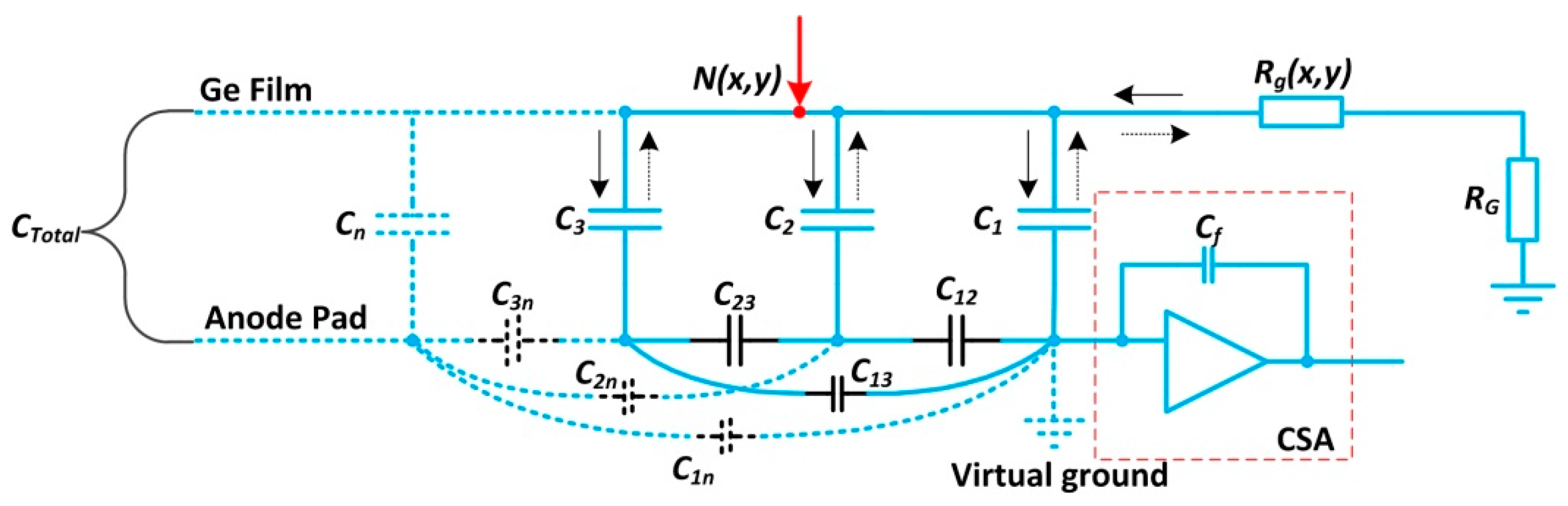
Figure 4 illuminates the simple model that describes the process of capacitor charge or discharge during charge induction.
N(x,y) indicates the node where the electron cloud lands on the germanium film.
C1,
C2 to
Cn represent the capacitances between the germanium film and each anode pad, respectively. The capacitor in the dotted line may exist in other types of readout anodes, such as the multi-anode and Vernier anode. Although the capacitances between the anode and reference points are usually ignored for the virtual ground node, the total capacitance between the germanium film and the reference points is dependent on the inter-electrode capacitances of charge division anodes in the black line in addition to the capacitances
C1,
C2 to
Cn. For the charge release pathway,
Rg(x,y) is used to evaluate the resistance. This represents the resistance between any node
N(x,y) and the discharged resistance
RG located on the germanium film’s edge. Additionally, the readout circuits are shown in the red dotted box, where only one CSA is presented as an example.
The direction of the electron flow is indicated by the solid arrow when the capacitors are charged. Similarly, the opposite direction illustrates that the capacitors are discharging. The time constant
τrd, in which each localized charge arriving at the germanium film is dispersed, can be expressed as:
Given that
Tcr is the duration of the electron cloud at node
N(x,y) and
Tw is the arriving interval of the two continuous events, the time constant
τrd needs to be limited to the following range:
When τrd is more than ten times greater than Tcr, the charge collected by the germanium film can be fully coupled to the anode without any loss. Each charge pulse from the anode has approximately the same shape, retaining enough information for data analysis. In contrast, the charge on the germanium film can only be partially coupled to the anode, resulting in deterioration of the detector resolution regardless of the incident photon rates. On the other hand, the charge on the germanium film cannot be completely released when τrd is more than or equal to Tw. This effect can cause pulse pile-up when a subsequent charge is detected before previous photon events have decayed. An evaluation of the relation between τrd and Tw is significant in high incident photon rate applications.
Because the arriving interval of photon events conforms to the Poisson distribution [
17,
20], the probability of
N photoelectric pulses emanating from MCPs in time
t is derived:
where
is the average counting rate of photons, taking into account quantum efficiency.
The time interval between any two adjacent pulses entering the ideal counter is not less than
τrd, and the counting error at the readout anode can, thus, be derived:
To reduce the counting error in high counting rate applications, it is necessary to thoroughly analyze the response time of other units of the detection system and not only the readout link, as discussed in the following sections.
2.3. Response of Readout Circuits
The photon counting technique’s performance for aurora detection also depends on the electronic system’s capacity to separate serial events [
21]. The topology of readout circuits is essential in achieving a low-noise detection system with a wide dynamic range.
Figure 5 provides an overview of the readout circuits’ overall architecture with the different modules involved, which was developed for space-borne observations considering the wedge strip anode in
Figure 3. Each channel consists of one CSA encapsulated in the shielding house with a photon counting imaging detector followed by the pulse shaper, which is usually implemented with two-stage RC networks to form a quasi-Gaussian pulse, and finally the A/D converter with a peak holder. In addition, the pulse pile-up rejection component sums up output voltages from three CSAs and then compares them with the upper or lower threshold level. If the total pulse amplitude triggers the threshold voltage, the corresponding state signal can be set. According to the time interval of this state signal, we can determine whether pulse pile-up events occur. Therefore, a few events may be rejected when successive pulses occur close to each other. The operations of threshold regulation, data acquisition and calculation, and logical control are also performed in the field programmable gate array (FPGA).
The response time of readout circuits is primarily determined by the rise time of the CSA and the time constant of the pulse shaper; the response time, in turn, affects the linear and dynamic range of the detection system. During the whole photoelectric event, the electron cloud is swept into the electrodes and subsequently gives rise to a current pulse with a time duration in the order of nanoseconds. To minimize the possibility of current pulses overlapping, a fast response characteristic is usually required of the CSA. The CSA is an essential component in the front end of analogue signal processing chains [
22].
As illustrated in
Figure 6, the CSA consists of an operational transconductance amplifier (OTA), a feedback resistor
Rf, a feedback capacitor
Cf and a load capacitance
CL [
12]. The MCP detector is modeled as a capacitor
CD in parallel with the anode’s current pulse
ID. The total capacitance
Cin on the OTA’s virtual ground node is approximately equal to the sum of the detector capacitance
CD, stray capacitance
Cs and OTA input capacitance
Ci.
Once a pulse of induced charge from MCP output appears on the virtual ground node, the step voltage at the CSA output is created by the feedback capacitor Cf as a result of the feedback operation. Afterwards, the charged capacitor Cf can be reset by the feedback resistor Rf until the next event arrives. An exponential decay follows the output voltage’s peak point, while the feedback resistor Rf brings the CSA back to its steady-state.
The current flow is illustrated in
Figure 7 to evaluate the characteristics of the CSA. The current
if flows through the feedback network, which determines the output voltage associated with the current
io. To achieve a high slew rate for the CSA’s output voltage, a sufficiently large
gm is expected to generate a huge output current
io.
According to the Kirchhoff current law (KCL) and the Kirchhoff voltage law (KVL), we can derive:
where
ID is the anode current from the detector,
iin is the current flowing into the total capacitance
Cin of the virtual ground node,
gm stands for the transconductance value of the OTA and
iL corresponds to the current flowing into the load capacitance
CL.
The transimpedance function
H(s)CSA, which establishes a connection between the CSA output voltage
Vout and the anode current
ID from the detector, is given as follows:
For sufficiently high transconductance
gm, the
H(s)CSA, which does not take into account
1/gm and
(CL + CD)/gmCf, is given as follows:
The transimpedance function
H(s)CSA possesses dominant poles at
1/RfCf and non-dominant poles at
. The high-frequency zeros at
gm/Cf can be ignored. The approximate value of the
H(s)CSA is equal to
1/
sCf between the dominant and non-dominant pole frequencies. Therefore, an application with a smaller feedback capacitance may achieve a higher output voltage for a low-input charge. The CSA’s conversion factor can be conducted with the feedback capacitance, whereas the rise time is normally constrained by the non-dominant pole. The rise time
tr of the CSA is further derived:
To keep the non-dominant pole frequency sufficiently high, low input capacitances and load capacitances, as well as high OTA transconductance, are necessary. A moderate increase in Cf, when the charge sensitivity is in the acceptable range, further contributes to reducing the rise time tr.
The fast rising time of the CSA can reduce the accumulation of pulses at the rising edge, which is conducive to improving the system’s counting capacity. The feedback resistor
Rf of the CSA is typically large in order to improve the charge collection efficiency. Nevertheless, the feedback resistor
Rf with shunt capacitance
Cf results in a long fall time of the CSA output, as shown in
Figure 6. In high counting rate applications, pulse pile-up would undoubtedly appear on the falling edge of the CSA output if the interval between two adjacent events was shorter than the fall time. To mitigate pulse pile-up, the CSA is usually followed by a pulse shaper, which can regulate the shape of the output pulse to reduce the fall time of the CSA output. Meanwhile, the smooth pulse generated by the pulse shaper improves the signal-to-noise ratio (SNR) of the analogue front-end chains. This modification facilitates the pulse amplitude measurement because the maximum is gradually rounded instead of steeple-shaped.
The pulse shaper consists of a C–R differentiator and an R–C integrator, which form a high-pass filter and a low-pass filter, as shown in
Figure 8. If a more symmetrical pulse is required for high SNR applications, the shaper’s order can be increased. As more than one R–C integrator is adopted, a quasi-Gaussian pulse can be generated at the shaper output end, which contains the timing and intensity information.
The transfer function of the pulse shaper is given as follows:
where
n is the number of R–C integrators that corresponds to the pulse shaper’s order,
τL is the time constant of the differentiator and
τH is the time constant of the integrator.
The time constant of the differentiator and the time constant of the integrator, taking the schematic parameters in
Figure 8 as an example, are given as follows:
where
fH and
fL are the high cut-off frequency and the low cut-off frequency of the pulse shaper, respectively.
The fall time of the shaped pulse at the output end of the pulse shaper is generally shorter than that of the CSA, which can be regulated by the high cut-off frequency. Similarly, the rise time of the shaped pulse is normally governed by the low cut-off frequency.
Assuming
RiCi =
RdCd, the correlation between the peaking time
τp of the shaped pulse and the time constant
τshaper is given as follows:
Increasing the pulse shaper’s order will result in a larger peaking time τp for the shaped pulse. The duration of the shaped pulse may exceed the interval between the arrival times of the two continuous photocurrent pulses. In this case, the pulse pile-up will occur again. Therefore, the peaking time needs to be adjusted to avoid pulse overlap as much as possible, and a fast pulse shaper is usually used for high counting rate applications. However, it is arduous to circumvent the pile-up of pulses on account of random pulse intervals. There are always counting errors, and the error of the pulse shaper can also be elucidated using Equation (5).
The entire detection system’s counting error can typically be described by the time factor
τtotal [
23]. The time factor
τtotal is further considered as the cumulative response time contributed by each time constant of the signal pathway. Taking the above analysis as an example, the time factor
τtotal can be calculated as:
where
τrd is the release time of the induced charge,
tr is the CSA’s response time and
τshaper is the time constant of the pulse shaper. The total time constant
τtotal characterizes the response speed of the system. The margin of error for a high counting rate system can be further evaluated according to the accuracy requirements of object detection.


