Polarization-Sensitive and Wide Incidence Angle-Insensitive Fabry–Perot Optical Cavity Bounded by Two Metal Grating Layers

 , ,
, ,  and
and 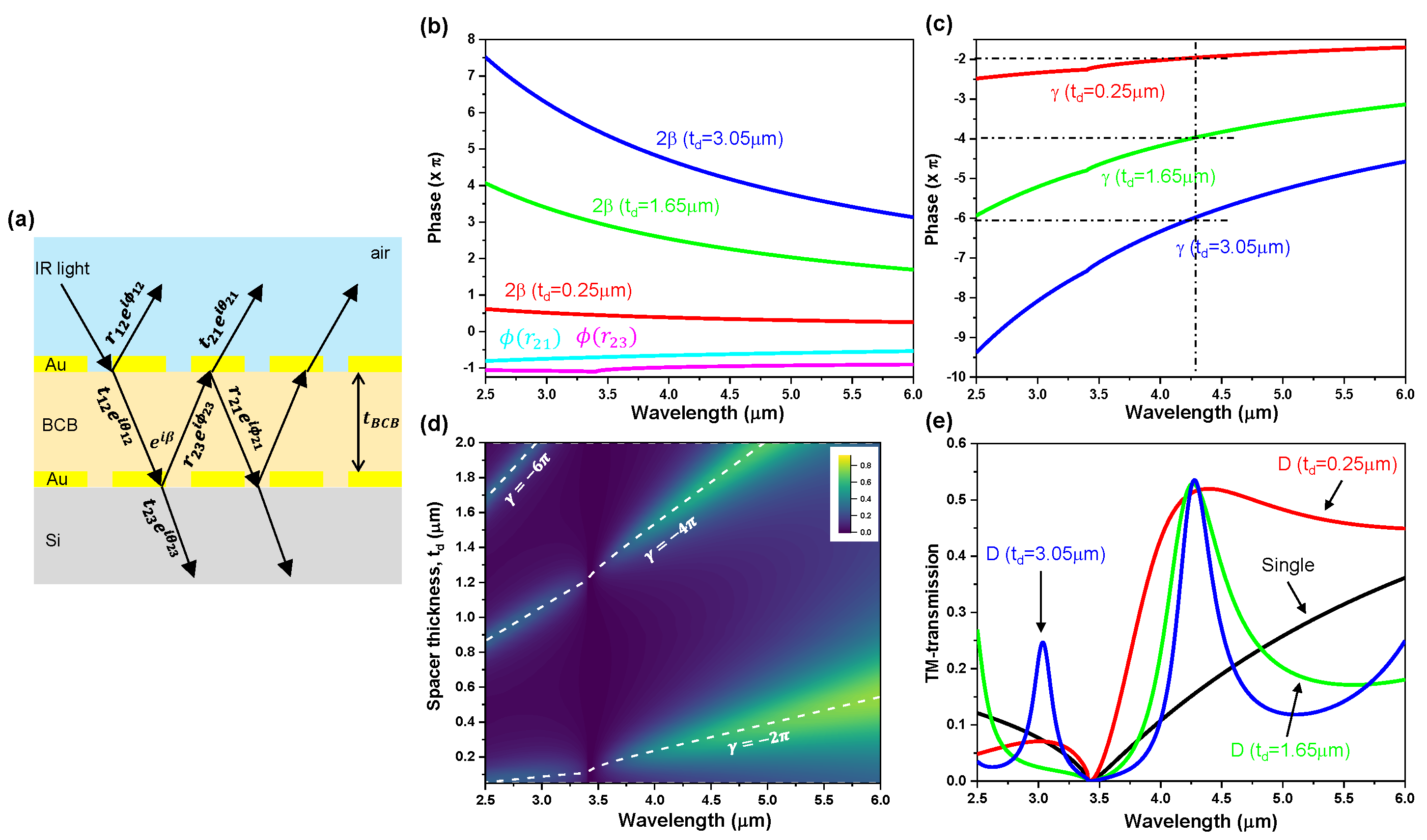
Abstract
1. Introduction
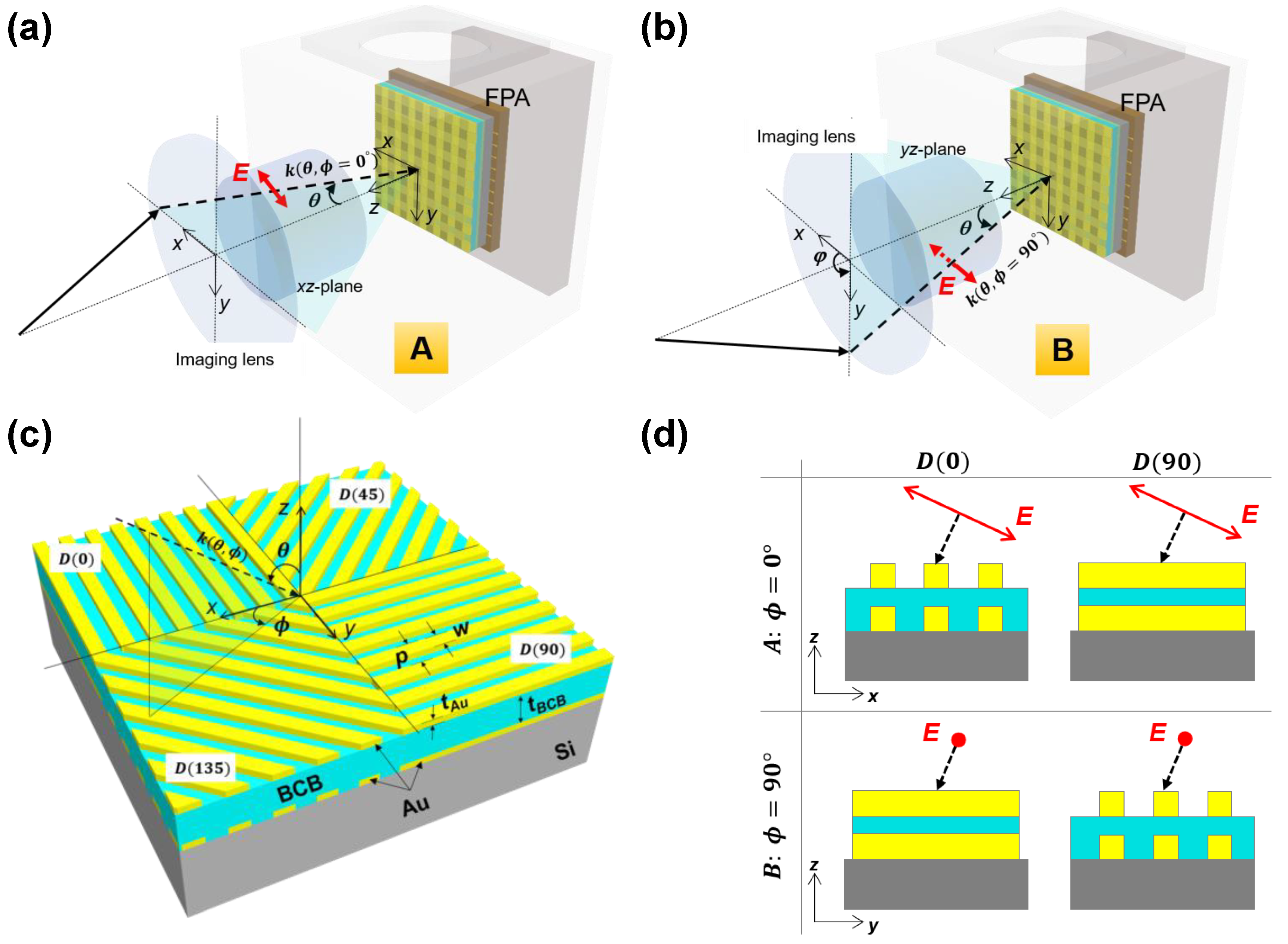
2. Design of Double-Layer Grating Using a Multiple-Layer Model
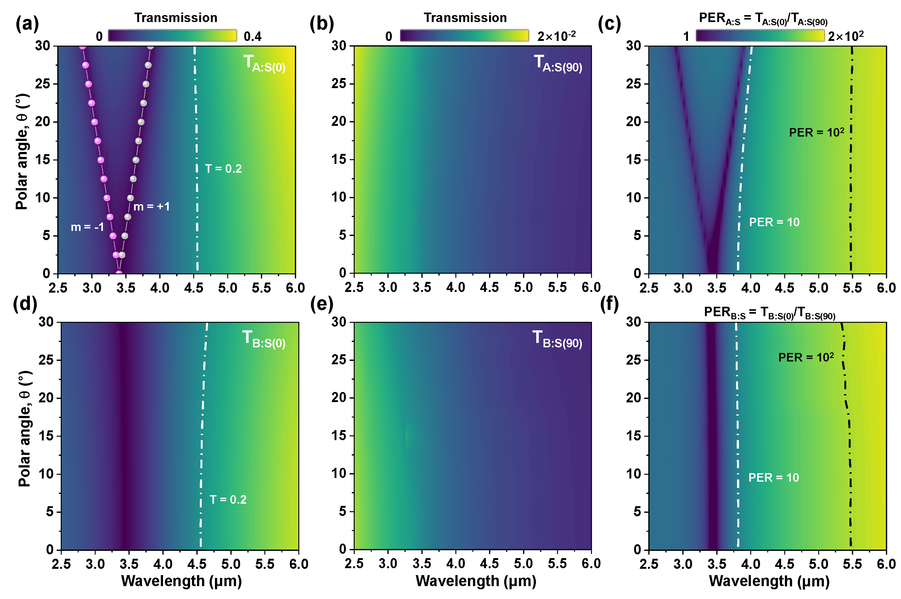
3. Theoretical Analysis of Incidence Angle-Dependent Polarization Sensitivity and PER of Double (Single)-Layer Au Grating
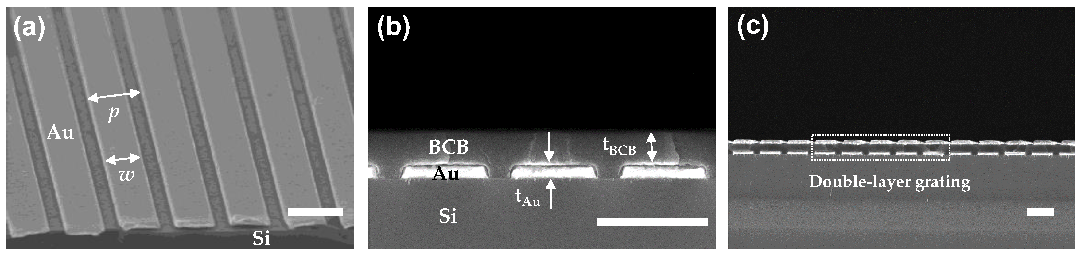
4. Polarization Sensitivity Measurement of NIL-Fabricated Double (Single)-Layer Grating
5. Conclusions
Author Contributions
Funding
Conflicts of Interest
Appendix A


References
- Tyo, J.S.; Goldstein, D.L.; Chenault, D.B.; Shaw, J.A. Review of passive imaging polarimetry for remote sensing applications. Appl. Opt. 2006, 45, 5453–5469. [Google Scholar] [CrossRef] [PubMed]
- Rogne, T.J.; Smith, F.G.; Rice, J.E. Passive target detection using polarized components of infrared signatures. Proc. Soc. Photo Opt. Instrum. Eng. 1990, 1317, 242–251. [Google Scholar]
- Shaw, J.A. Degree of linear polarization in spectral radiances from water-viewing infrared radiometers. Appl. Opt. 1999, 38, 3157–3165. [Google Scholar] [CrossRef] [PubMed]
- Salomatina-Mottsa, E.; Neela, V.A.; Yaroslavskaya, A.N. Multimodal polarization system for imaging skin cancer. Opt. Spectrosc. 2009, 107, 884–890. [Google Scholar] [CrossRef]
- Ogawa, S.; Kimata, M. Wavelength-or polarization-selective thermal infrared detectors for multi-color or polarimetric imaging using plasmonics and metamaterials. Materials 2017, 10, 493. [Google Scholar] [CrossRef]
- Felton, M.; Gurton, K.P.; Pezzaniti, J.L.; Chenault, D.B.; Roth, L.E. Measured comparison of the crossover periods for mid-and long-wave IR (MWIR and LWIR) polarimetric and conventional thermal imagery. Opt. Express 2010, 18, 15704–15713. [Google Scholar] [CrossRef]
- Gurton, K.P.; Yuffa, A.J.; Videen, G.W. Enhanced facial recognition for thermal imagery using polarimetric imaging. Opt. Lett. 2014, 39, 3857–3859. [Google Scholar] [CrossRef] [PubMed]
- Nee, T.W.; Nee, S.M.F. Infrared polarization signatures for targets. Proc. Soc. Photo Opt. Instrum. Eng. 2005, 2469, 231–241. [Google Scholar]
- Wilson, J.P.; Schuetz, C.A.; Dillon, T.E.; Eng, D.L.K.; Prather, D.W.; Dillon, T.E. Display of polarization information for passive millimeter-wave imagery millimeter-wave imagery. Opt. Eng. 2012, 51, 091607. [Google Scholar] [CrossRef]
- Gurton, K.P.; Dahmani, R. Effect of surface roughness and complex indices of refraction on polarized thermal emission. Appl. Opt. 2005, 44, 5361–5367. [Google Scholar] [CrossRef] [PubMed]
- Lewis, G.D.; Jordan, D.L.; Roberts, P.J. Backscattering target detection in a turbid medium by polarization discrimination. Appl. Opt. 1999, 38, 3937–3944. [Google Scholar] [CrossRef] [PubMed]
- Tyo, J.S.; Ratliff, B.M.; Boger, J.K.; Black, W.T.; Bowers, D.L.; Fetrow, M.P.; Air, U.S.; Se, A.; Afb, K. The effects of thermal equilibrium and contrast in LWIR polarimetric images. Opt. Express 2007, 15, 15161–15167. [Google Scholar] [CrossRef] [PubMed]
- Nordin, G.P.; Meier, J.T.; Deguzman, P.C.; Jones, M.W. Micropolarizer array for infrared imaging polarimetry. J. Opt. Soc. Am. A 1999, 16, 1168–1174. [Google Scholar] [CrossRef]
- Andreou, A.G.; Kalayjian, Z.K. Polarization imaging: Principles and integrated polarimeters. IEEE Sens. J. 2002, 2, 566–576. [Google Scholar] [CrossRef]
- Gruev, V.; Perkins, R.; York, T. CCD polarization imaging sensor with aluminum nanowire optical filters. Opt. Express 2010, 18, 19087–19094. [Google Scholar] [CrossRef]
- Perkins, R.; Gruev, V. Signal-to-noise analysis of Stokes parameters in division of focal plane polarimeters. Opt. Express 2010, 18, 25815–25824. [Google Scholar] [CrossRef] [PubMed]
- Antoni, T.; Nedelcu, A.; Marcadet, X.; Facoetti, H.; Berger, V. High contrast polarization sensitive quantum well infrared photodetectors. Appl. Phys. Lett. 2007, 90, 201107. [Google Scholar] [CrossRef]
- Apalkov, V.; Ariyawansa, G.; Perera, A.G.U.; Buchanan, M.; Wasilewski, Z.R.; Liu, H.C. Polarization Sensitivity of Quantum Well Infrared Photodetector Coupled to a Metallic Diffraction Grid. IEEE J. Quantum Electron 2010, 46, 877–883. [Google Scholar] [CrossRef]
- Wang, R.; Li, T.; Shao, X.; Li, X.; Gong, H. The simulation of localized surface plasmon and surface plasmon polariton in wire grid polarizer integrated on InP substrate for InGaAs sensor. AIP Adv. 2015, 5, 077128. [Google Scholar] [CrossRef]
- Li, Q.; Li, Z.; Li, N.; Chen, X.; Chen, P.; Shen, X.; Lu, W. High-polarization-discriminating infrared detection using a single quantum well sandwiched in plasmonic micro-cavity. Sci. Rep. 2014, 4, 6332. [Google Scholar] [CrossRef]
- Young, J.B.; Graham, H.A.; Peterson, E.W. Wire grid infrared polarizer. Appl. Opt. 1965, 4, 1023–1026. [Google Scholar] [CrossRef]
- Porto, J.A.; Garc’ıa-Vidal, F.J.; Pendry, J.B. Transmission Resonances on Metallic Gratings with Very Narrow Slits. Phys. Rev. Lett. 1999, 83, 2845–2848. [Google Scholar] [CrossRef]
- Lalanne, P.; Hugonin, J.P.; Rodier, J.C. Theory of surface plasmon generation at nanoslit apertures. Phys. Rev. Lett. 2005, 95, 263902. [Google Scholar] [CrossRef] [PubMed]
- Pang, Y.; Genet, C.; Ebbesen, T.W. Optical transmission through subwavelength slit apertures in metallic films. Opt. Commun. 2007, 280, 10–15. [Google Scholar] [CrossRef]
- Chan, H.B.; Marcet, Z.; Woo, K.; Tanner, D.B.; Carr, D.W.; Bower, J.E.; Pai, C.S. Optical transmission through double-layer metallic subwavelength slit arrays. Opt. Lett. 2006, 31, 516–518. [Google Scholar] [CrossRef]
- Tardieu, C.; Estruch, T.; Vincent, G.; Jaeck, J.; Bardou, N.; Collin, S.; Haïdar, R. Extraordinary optical extinctions through dual metallic gratings. Opt. Lett. 2015, 40, 661–664. [Google Scholar] [CrossRef]
- Huang, Z.; Parrott, E.P.J.; Park, H.; Chan, H.P.; Pickwell-MacPherson, E. High extinction ratio and low transmission loss thin-film terahertz polarizer with a tunable bilayer metal wire-grid structure. Opt. Lett. 2014, 39, 793–796. [Google Scholar] [CrossRef]
- Al, B.; Ekinci, Y.; Solak, H.H.; David, C.; Sigg, H. Bilayer Al wire-grids as broadband and high- performance polarizers. Opt. Express 2006, 14, 2323–2334. [Google Scholar]
- York, T.; Gruev, V. Characterization of a visible spectrum division-of-focal-plane polarimeter. Appl. Opt. 2012, 51, 5392–5400. [Google Scholar] [CrossRef]
- Ratliff, B.M.; Lacasse, C.F.; Tyo, J.S. Interpolation strategies for reducing IFOV artifacts in microgrid polarimeter imagery. Opt. Express 2009, 17, 9112–9125. [Google Scholar] [CrossRef]
- Tyo, J.S.; Lacasse, C.F.; Ratliff, B.M. Total elimination of sampling errors in polarization imagery obtained with integrated microgrid polarimeters. Opt. Lett. 2009, 34, 3187–3189. [Google Scholar] [CrossRef]
- Gao, S.; Gruev, V. Image interpolation methods evaluation for division of focal plane polarimeters. Proc. SPIE Int. Soc. Opt. Eng. 2011, 8012, 80120N. [Google Scholar]
- Gao, S.; Gruev, V. Bilinear and bicubic interpolation methods for division of focal plane polarimeters. Opt. Express 2011, 19, 26161–26173. [Google Scholar] [CrossRef]
- Gao, S.; Gruev, V. Gradient-based interpolation method for division-of-focal-plane polarimeters. Opt. Express 2013, 21, 1137–1151. [Google Scholar] [CrossRef] [PubMed]
- LeMaster, D.A.; Hirakawa, K. Improved microgrid arrangement for integrated imaging polarimeters. Opt. Lett. 2014, 39, 1811–1814. [Google Scholar] [CrossRef] [PubMed]
- Zhao, X.; Lu, X.; Abubakar, A.; Bermak, A. Novel micro-polarizer array patterns for CMOS polarization image sensors. In Proceedings of the 5th International Conference on Electronic Devices, Systems and Applications, Ras Al Khaimah, UAE, 6–8 December 2016; pp. 1–4. [Google Scholar]
- Vaughn, I.J.; Alenin, A.S.; Tyo, J.S. Channeled spatio–temporal stokes polarimeters. Opt. Lett. 2018, 43, 2768–2771. [Google Scholar] [CrossRef] [PubMed]
- Zhang, J.; Ye, W.; Ahmed, A.; Qiu, Z.; Cao, Y.; Zhao, X. A novel smoothness-based interpolation algorithm for division of focal plane Polarimeters. In Proceedings of the IEEE International Symposium on Circuits and Systems, Baltimore, MA, USA, 28–31 May 2017; pp. 1–4. [Google Scholar]
- Li, N.; Zhao, Y.; Pan, Q.; Kong, S.G. Demosaicking DoFP images using Newton′s polynomial interpolation and polarization difference model. Opt. Express 2019, 27, 1376–1391. [Google Scholar] [CrossRef]
- Zhang, J.; Luo, H.; Hui, B.; Chang, Z. Image interpolation for division of focal plane polarimeters with intensity correlation. Opt. Express 2016, 24, 20799–20807. [Google Scholar] [CrossRef]
- Zhang, J.; Shao, J.; Luo, H.; Zhang, X.; Hui, B.; Chang, Z.; Liang, R. Learning a convolutional demosaicing network for microgrid polarimeter imagery. Opt. Lett. 2018, 43, 4534–4537. [Google Scholar] [CrossRef]
- Park, Y.; Lee, S.; Jeong, B.; Yoon, J. Joint Demosaicing and Denoising Based on a Variational Deep Image Prior Neural Network. Sensors 2020, 20, 2970. [Google Scholar] [CrossRef]
- Jiang, T.; Wen, D.; Song, Z.; Zhang, W.; Li, Z.; Wei, X.; Liu, G. Minimized Laplacian residual interpolation for DoFP polarization image demosaicking. Appl. Opt. 2019, 58, 7367–7374. [Google Scholar] [CrossRef] [PubMed]
- Zhang, J.; Luo, H.; Liang, R.; Ahmed, A.; Zhang, X.; Hui, B.; Chang, Z. Sparse representation-based demosaicing method for microgrid polarimeter imagery. Opt. Lett. 2018, 43, 3265–3268. [Google Scholar] [CrossRef] [PubMed]
- Jeon, J.; Bhattarai, K.; Kim, D.-K.; Kim, J.O.; Urbas, A.; Lee, S.J.; Ku, Z.; Zhou, J. A Low-loss Metasurface Antireflection Coating on Dispersive Surface Plasmon Structure. Sci. Rep. 2016, 6, 36190. [Google Scholar] [CrossRef] [PubMed]
- Bhattarai, K.; Silva, S.; Song, K.; Urbas, A.; Lee, S.J.; Ku, Z.; Zhou, J. Metamaterial Perfect Absorber Analyzed by a Meta-cavity Model Consisting of Multilayer Metasurfaces. Sci. Rep. 2017, 7, 10569. [Google Scholar] [CrossRef]
- Bhattarai, K.; Ku, Z.; Silva, S.; Jeon, J.; Kim, J.O.; Lee, S.J.; Zhou, J. A Large-Area, Mushroom-Capped Plasmonic Perfect Absorber: Refractive Index Sensing and Fabry–Perot Cavity Mechanism. Adv. Opt. Mater. 2015, 3, 1779–1786. [Google Scholar] [CrossRef]
- CST Studio Suite. Available online: https://www.3ds.com/products-services/simulia/products/cst-studio-suite/ (accessed on 19 September 2020).
- Ordal, M.A.; Long, L.L.; Bell, R.J.; Bell, S.E.; Bell, R.R.; Alexander, R.W.; Ward, C.A. Optical properties of the metals Al, Co, Cu, Au, Fe, Pb, Ni, Pd, Pt, Ag, Ti, and w in the infrared and far infrared. Appl. Opt. 1983, 22, 1099–1119. [Google Scholar] [CrossRef]
- COMSOL Multiphysics. Available online: https://www.comsol.com/ (accessed on 19 September 2020).


© 2020 by the authors. Licensee MDPI, Basel, Switzerland. This article is an open access article distributed under the terms and conditions of the Creative Commons Attribution (CC BY) license (http://creativecommons.org/licenses/by/4.0/).
Share and Cite
Hwang, J.; Ku, Z.; Jeon, J.; Kim, Y.; Kim, D.-K.; Kim, E.K.; Lee, S.J. Polarization-Sensitive and Wide Incidence Angle-Insensitive Fabry–Perot Optical Cavity Bounded by Two Metal Grating Layers. Sensors 2020, 20, 5382. https://doi.org/10.3390/s20185382
Hwang J, Ku Z, Jeon J, Kim Y, Kim D-K, Kim EK, Lee SJ. Polarization-Sensitive and Wide Incidence Angle-Insensitive Fabry–Perot Optical Cavity Bounded by Two Metal Grating Layers. Sensors. 2020; 20(18):5382. https://doi.org/10.3390/s20185382
Chicago/Turabian StyleHwang, Jehwan, Zahyun Ku, Jiyeon Jeon, Yeongho Kim, Deok-Kee Kim, Eun Kyu Kim, and Sang Jun Lee. 2020. "Polarization-Sensitive and Wide Incidence Angle-Insensitive Fabry–Perot Optical Cavity Bounded by Two Metal Grating Layers" Sensors 20, no. 18: 5382. https://doi.org/10.3390/s20185382
APA StyleHwang, J., Ku, Z., Jeon, J., Kim, Y., Kim, D.-K., Kim, E. K., & Lee, S. J. (2020). Polarization-Sensitive and Wide Incidence Angle-Insensitive Fabry–Perot Optical Cavity Bounded by Two Metal Grating Layers. Sensors, 20(18), 5382. https://doi.org/10.3390/s20185382