Wide Bandwidth Class-S Power Amplifiers for Ultrasonic Devices

Abstract
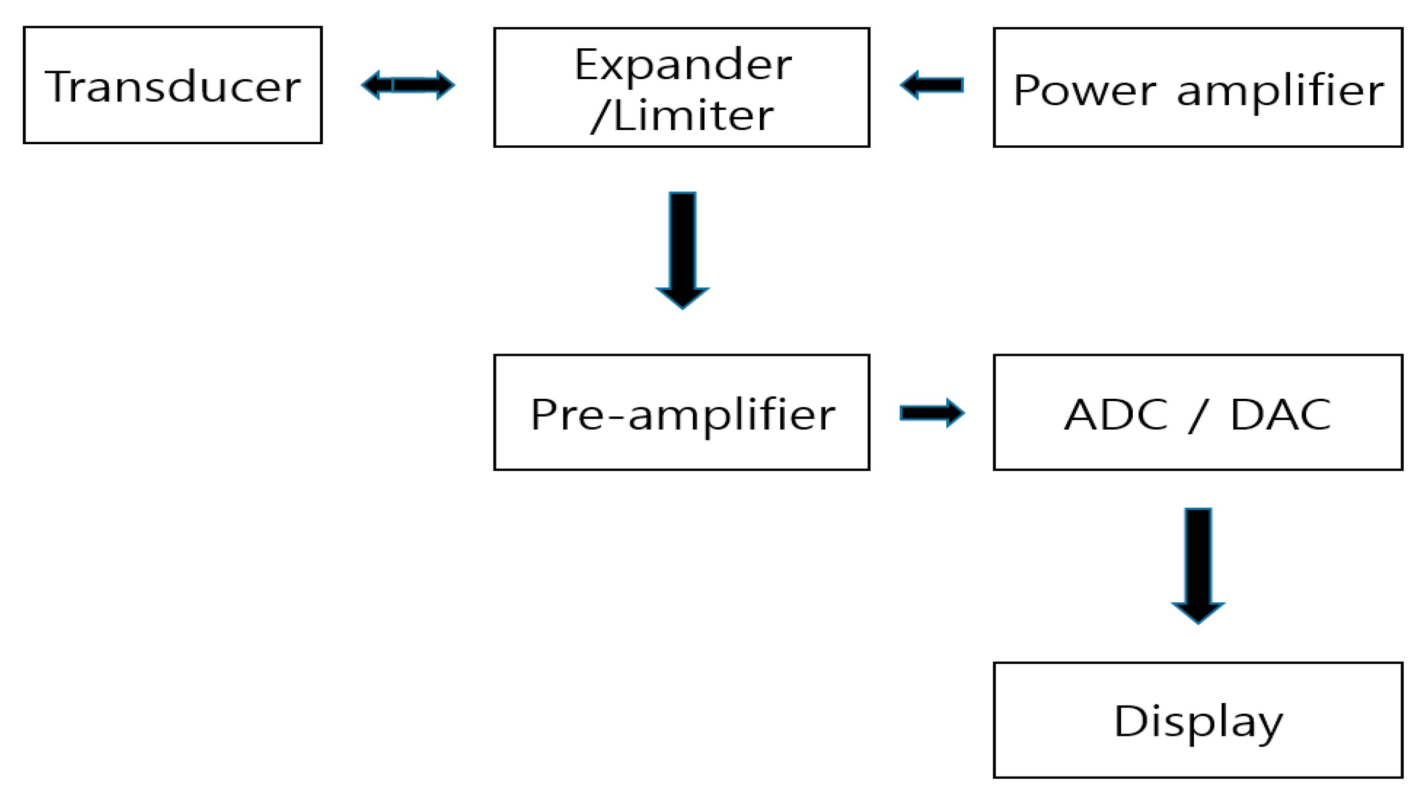
1. Introduction
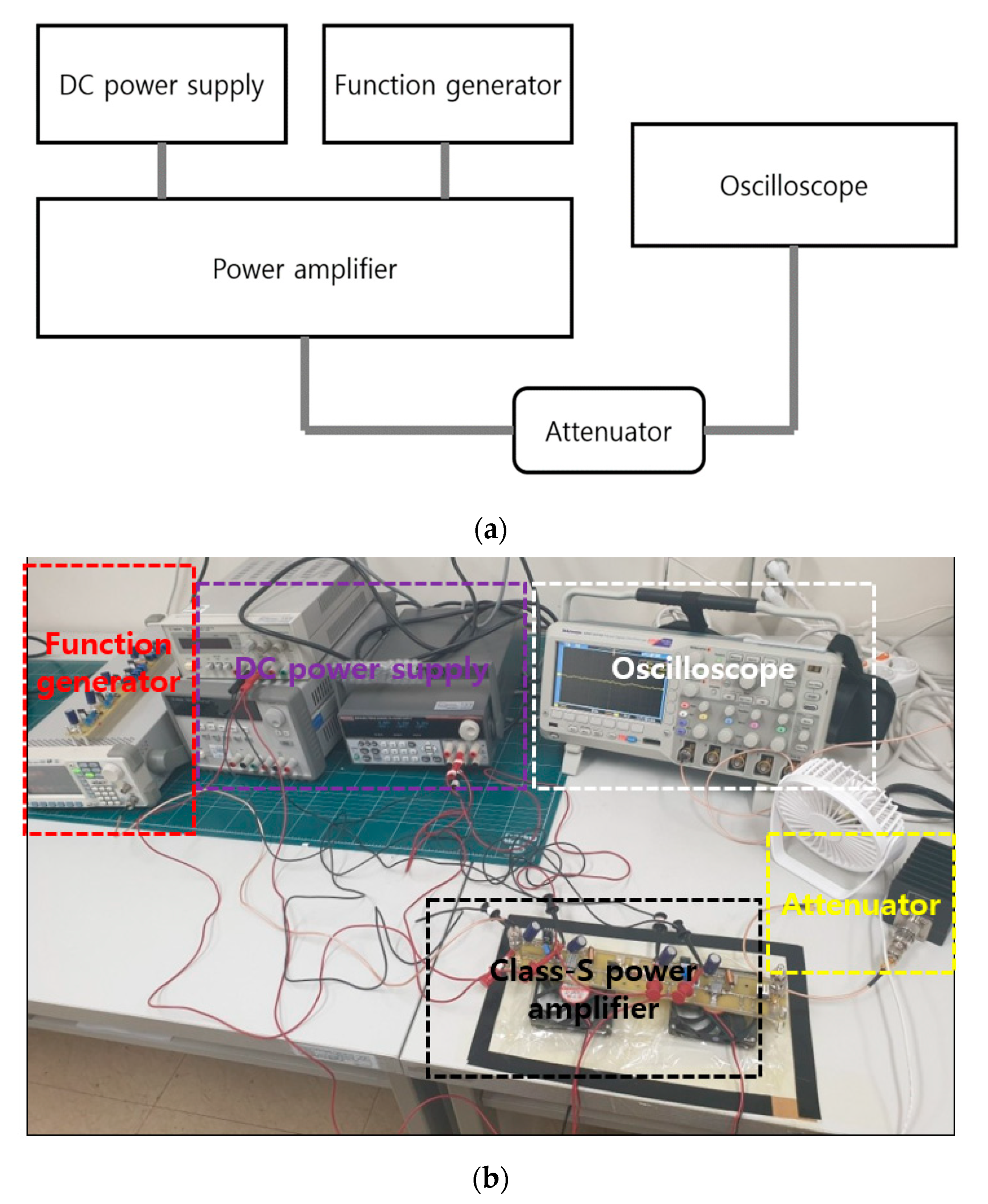
2. Materials and Methods
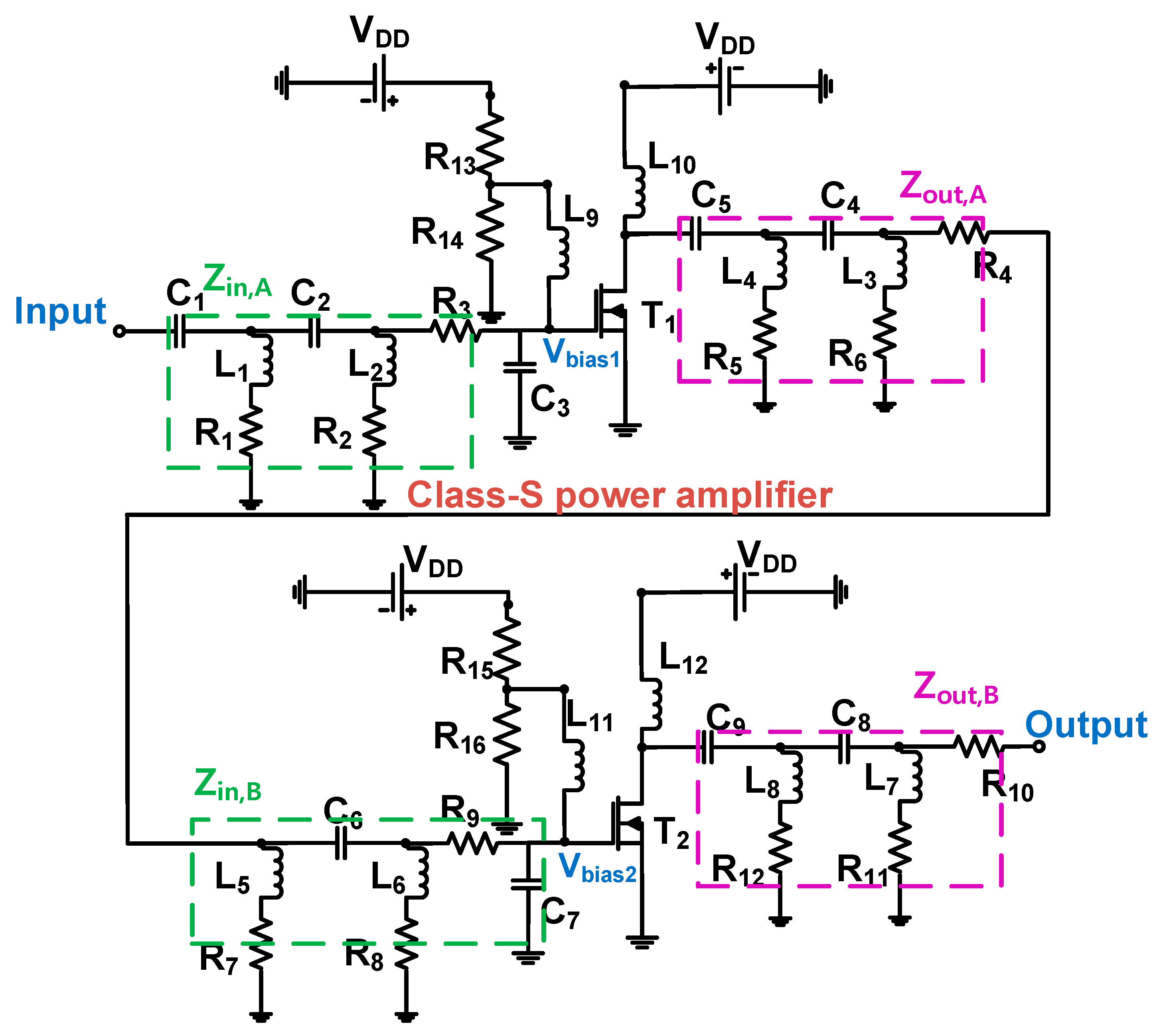
2.1. Schematic of the Class–S Power Amplifier
2.2. Analysis of the Class–S Power Amplifier
2.2.1. First Stage Power Amplifier
2.2.2. Second Stage Power Amplifier
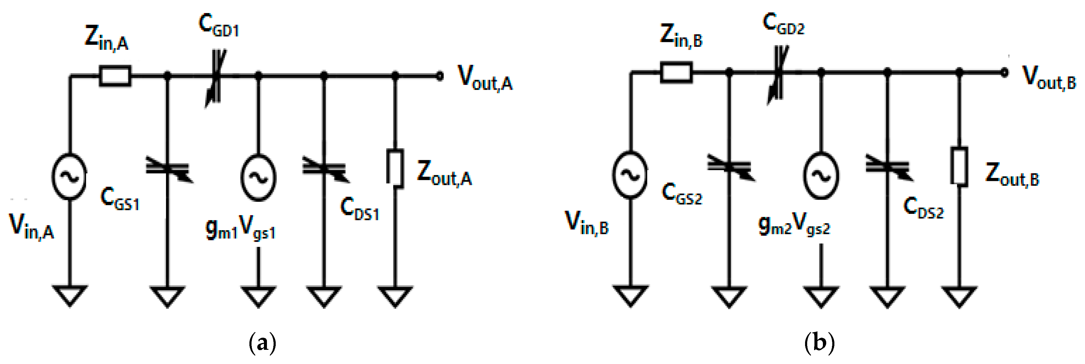
2.2.3. Equivalent Circuit Analysis of a Two-Stage Power Amplifier
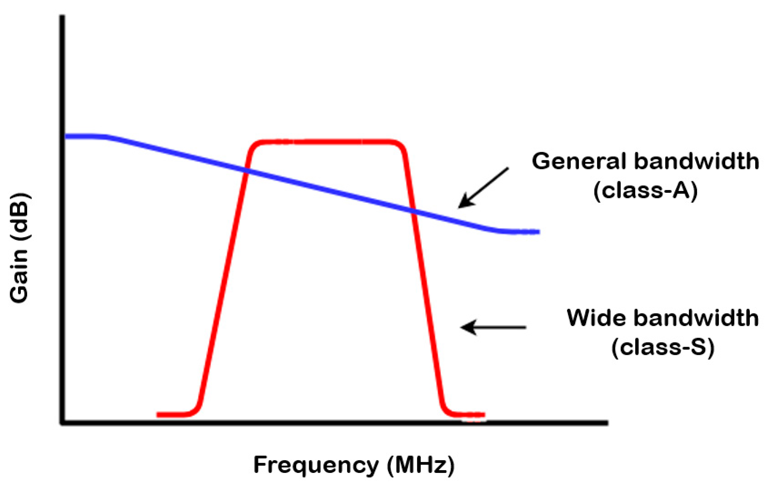
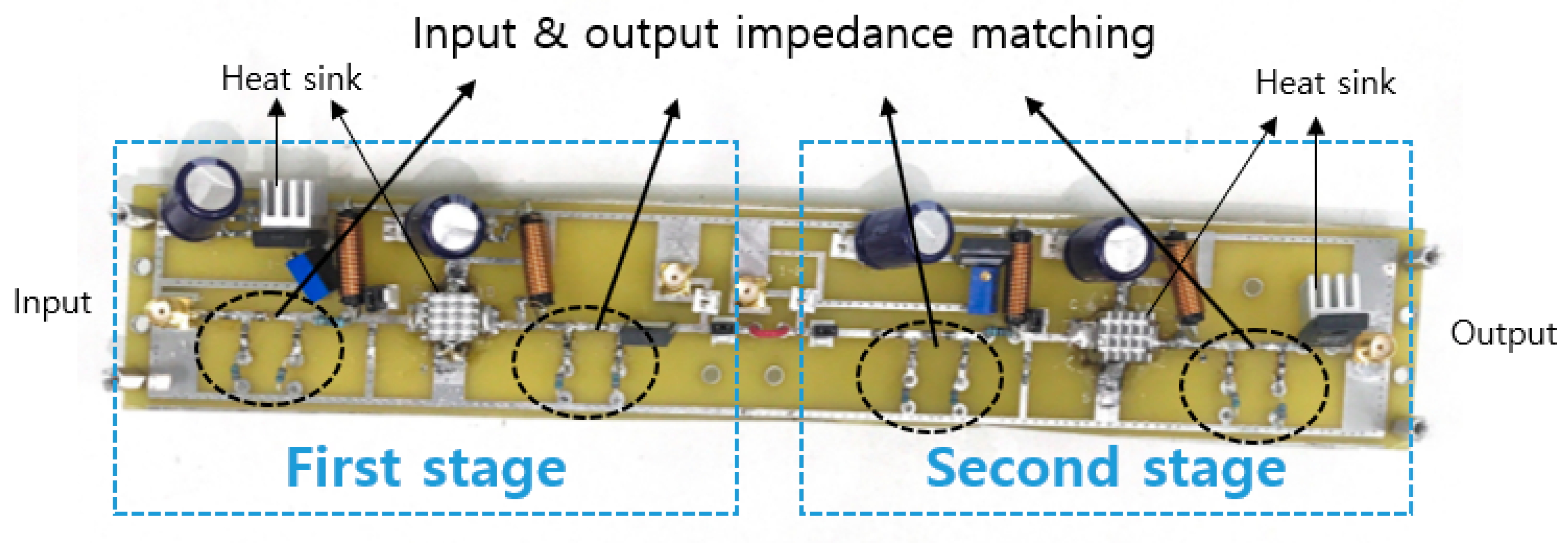
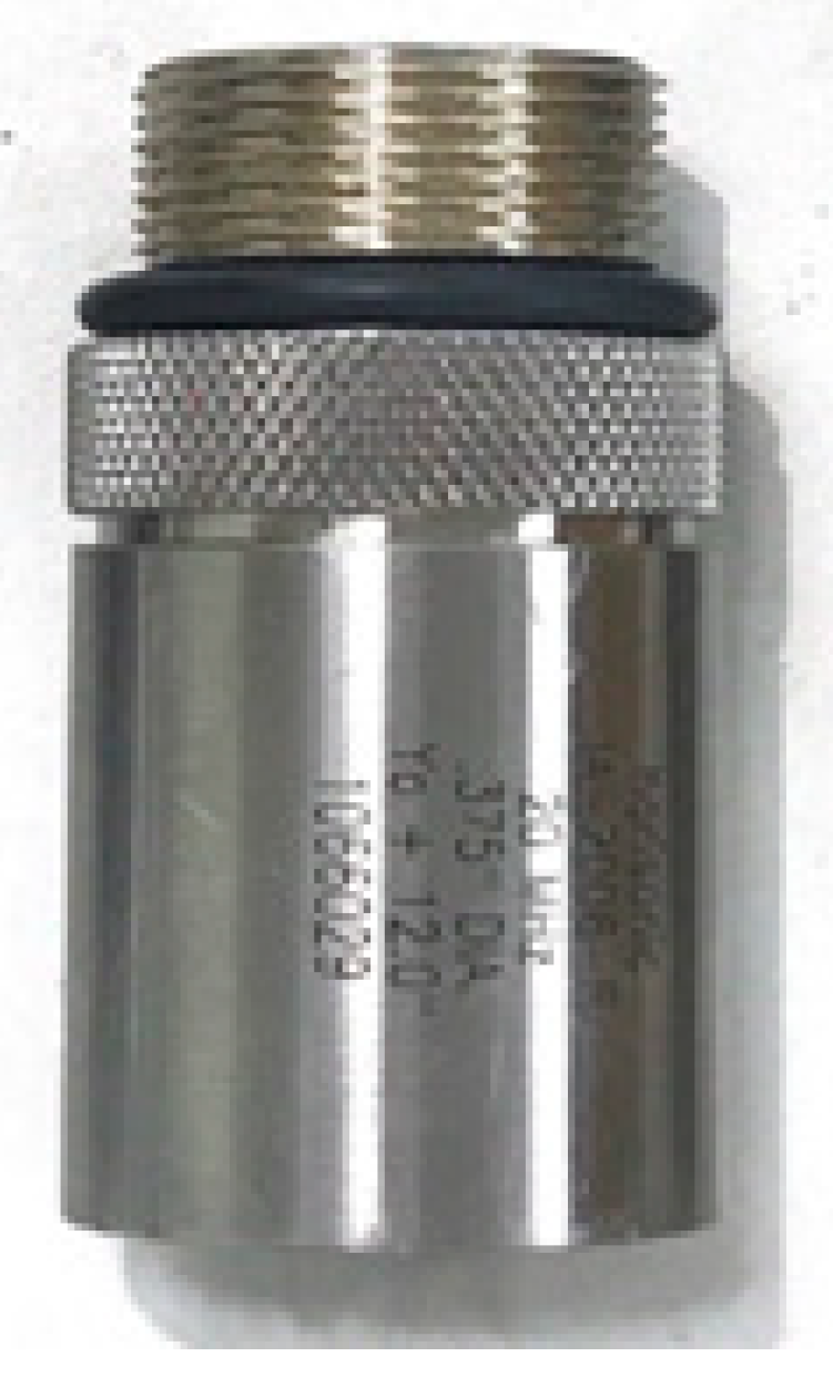
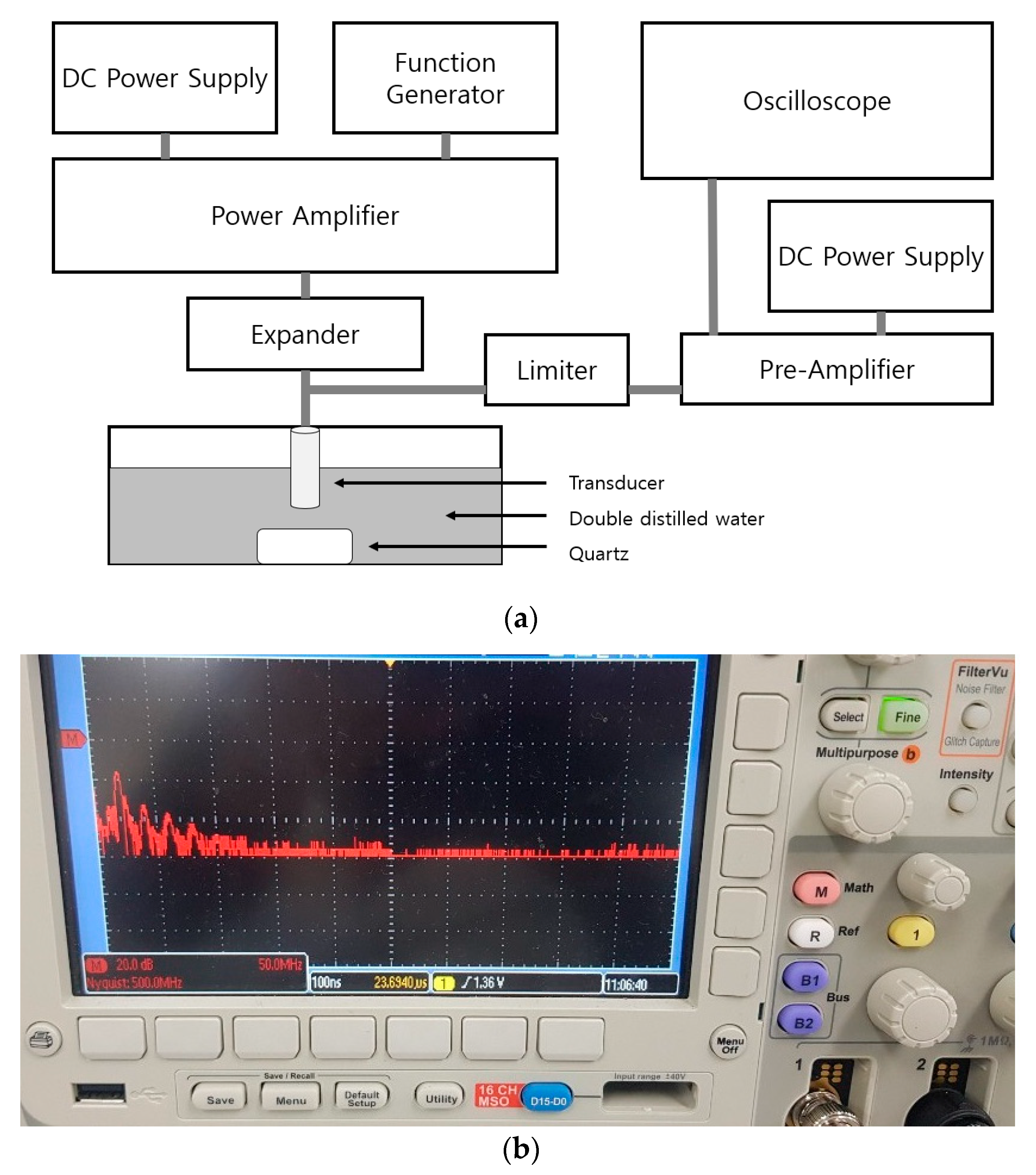
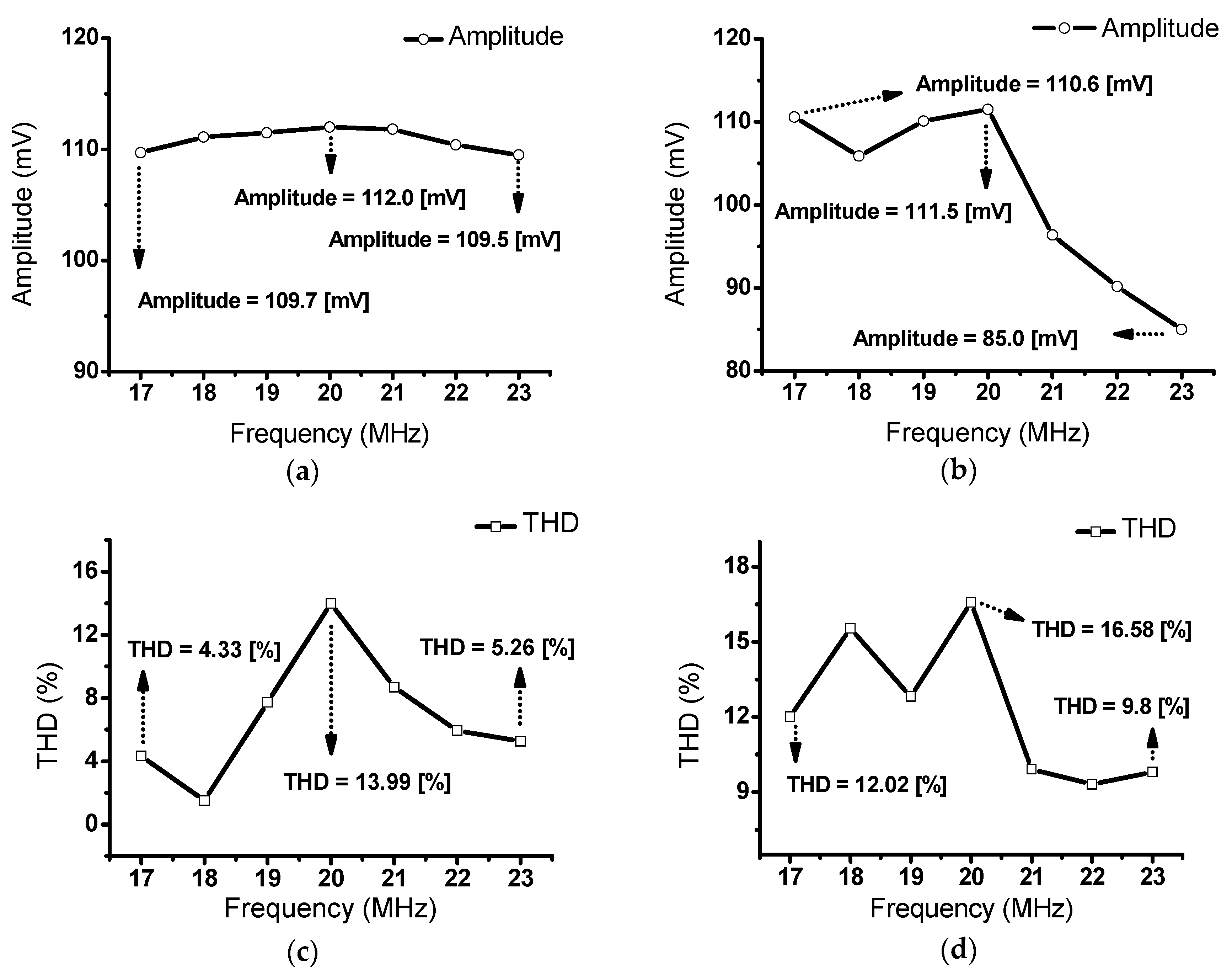
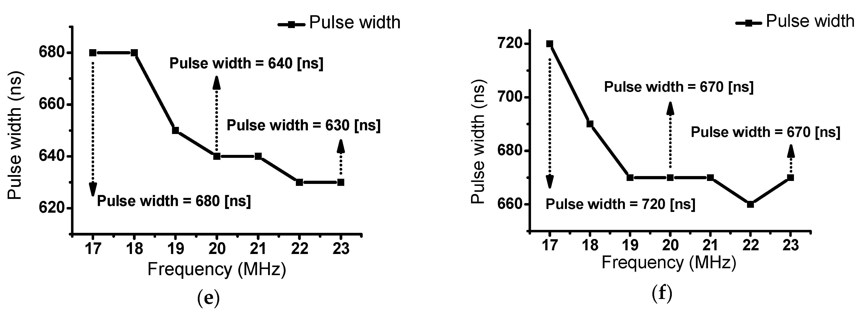
3. Results
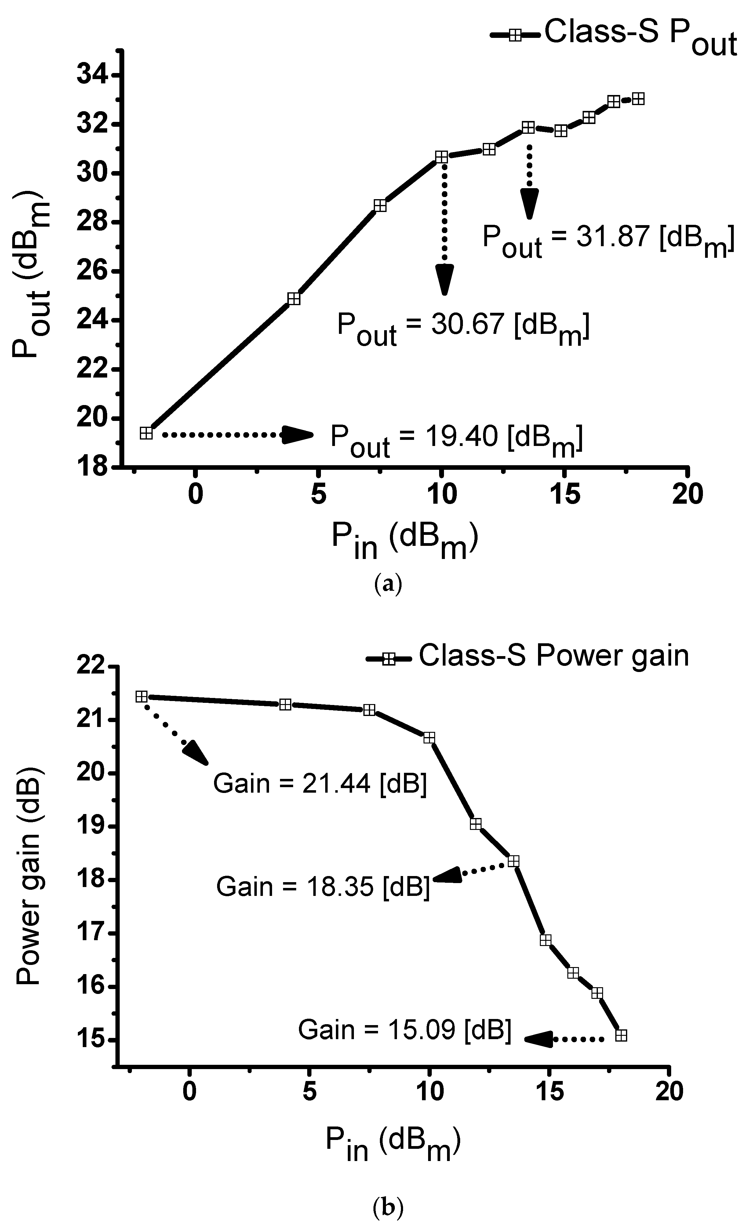
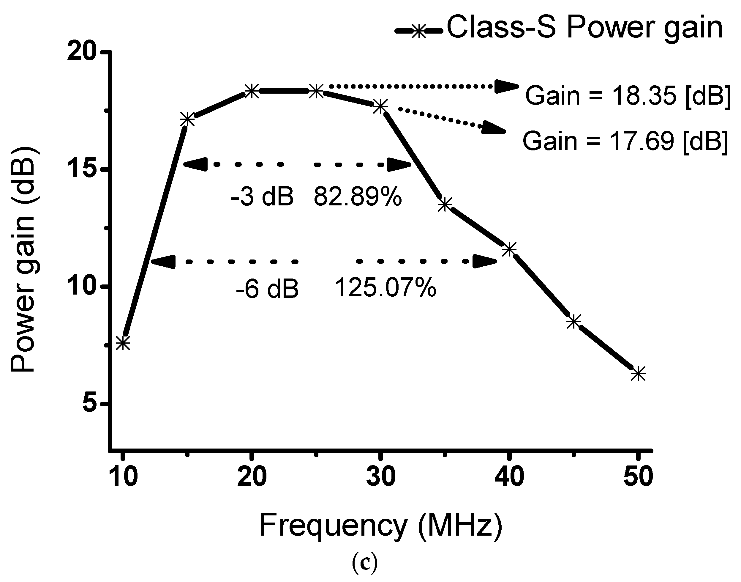
3.1. Performance Analysis
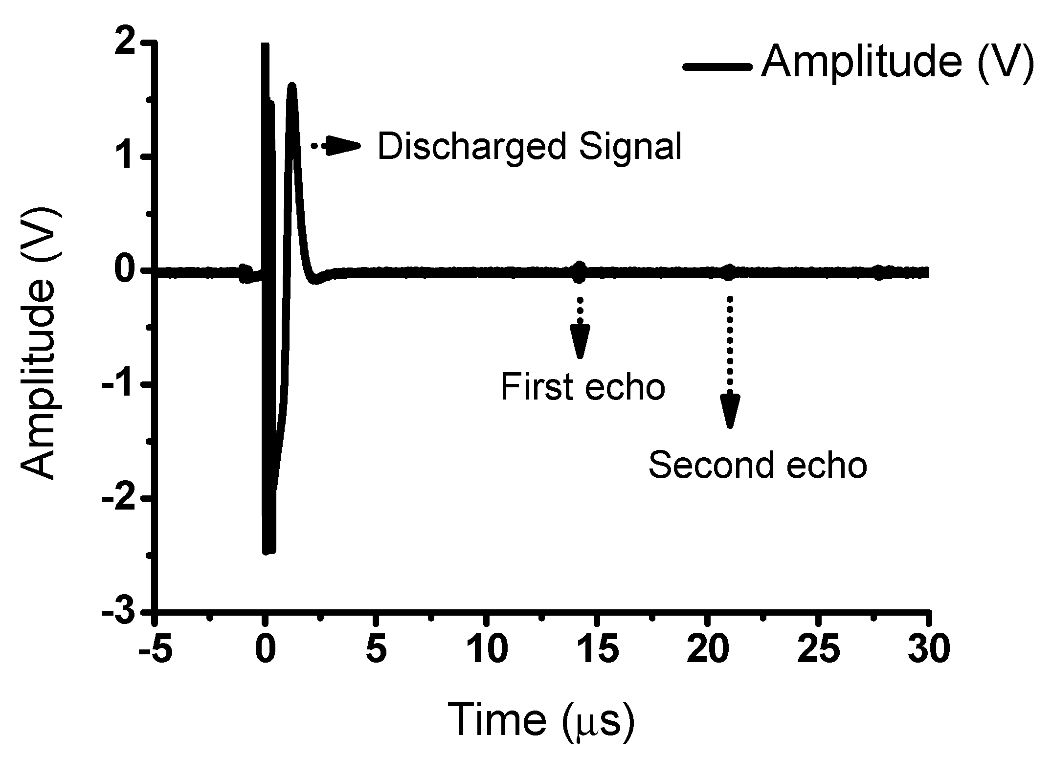
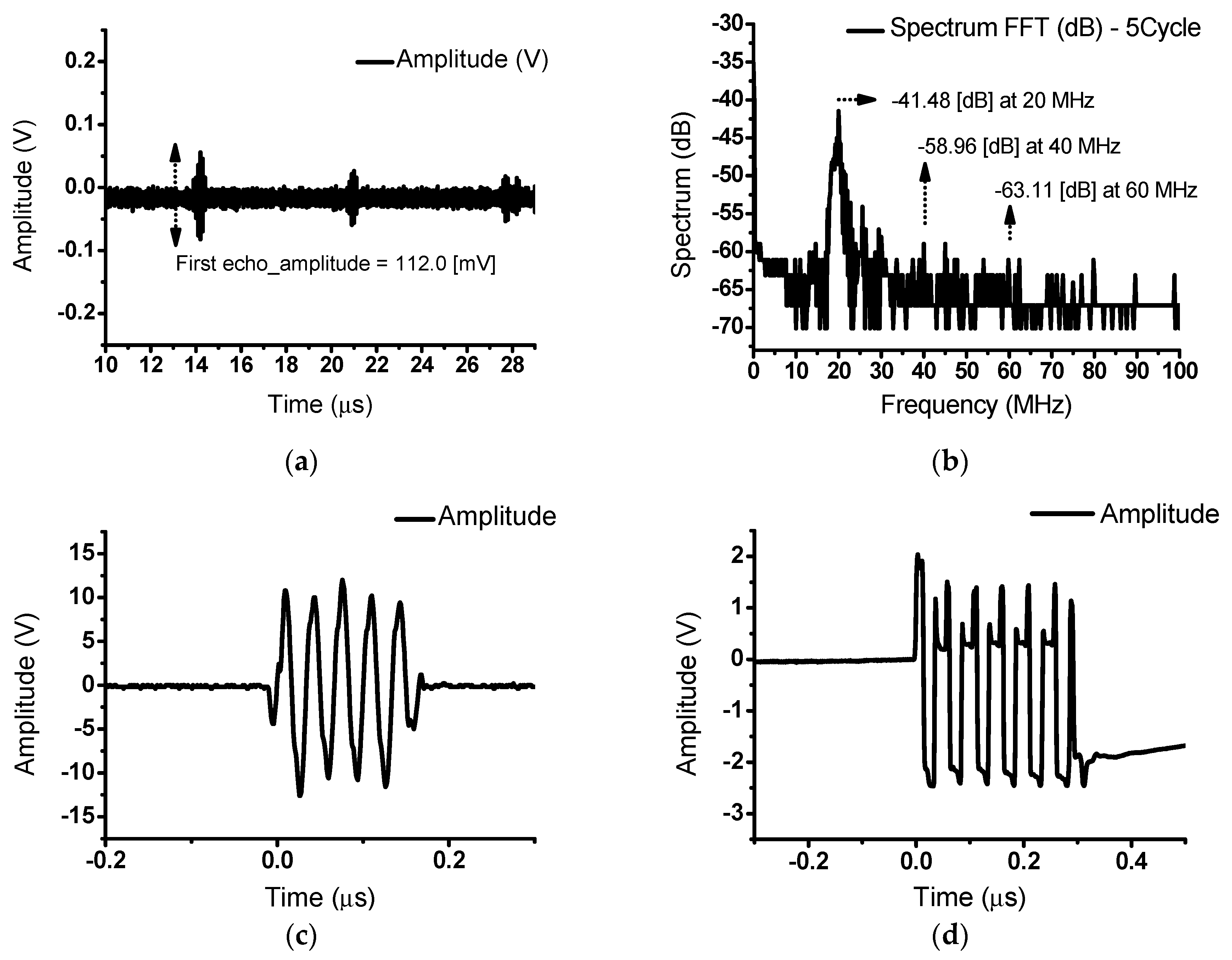
3.2. Pulse-Echo Analysis
4. Conclusions
Author Contributions
Funding
Conflicts of Interest
References
- Gallego-Juárez, J.A.; Graff, K.F. Power Ultrasonics: Applications of High-Intensity Ultrasound; Elsevier: Cambridge, UK, 2014. [Google Scholar]
- Choi, H.; Choe, S.-W. Acoustic Stimulation by Shunt-Diode Pre-Linearizer Using Very High Frequency Piezoelectric Transducer for Cancer Therapeutics. Sensors 2019, 19, 357. [Google Scholar] [CrossRef] [PubMed]
- Shin, S.-H.; Yoo, W.-S.; Choi, H. Development of modified RSA algorithm using fixed mersenne prime numbers for medical ultrasound imaging instrumentation. Technol. Health Care 2019, 24, 73–78. [Google Scholar] [CrossRef] [PubMed]
- Shin, S.-H.; Yoo, W.-S.; Choi, H. Development of Public Key Cryptographic Algorithm Using Matrix Pattern for Tele-Ultrasound Applications. Mathematics 2019, 7, 752. [Google Scholar] [CrossRef]
- Smith, N.B.; Webb, A. Introduction to Medical Imaging: Physics, Engineering and Clinical Applications; Cambridge University Press: Cambridge, UK, 2010. [Google Scholar]
- Choi, H. Prelinearized Class-B Power Amplifier for Piezoelectric Transducers and Portable Ultrasound Systems. Sensors 2019, 19, 287. [Google Scholar] [CrossRef] [PubMed]
- Leighton, T.G. What is ultrasound? Prog. Biophys. Mol. Biol. 2007, 93, 3–83. [Google Scholar] [CrossRef] [PubMed]
- Choi, H. Stacked Transistor Bias Circuit of Class-B Amplifier for Portable Ultrasound Systems. Sensors 2019, 19, 5252. [Google Scholar] [CrossRef]
- Kremkau, F.W.; Forsberg, F. Sonography Principles and Instruments; Elsevier Health Sciences: Amsterdam, The Netherlands, 2015. [Google Scholar]
- Choi, H.; Park, C.; Kim, J.; Jung, H. Bias-Voltage Stabilizer for HVHF Amplifiers in VHF Pulse-Echo Measurement Systems. Sensors 2017, 17, 2425. [Google Scholar] [CrossRef]
- Brunner, E. Ultrasound system considerations and their impact on front-end components. Analog Devices 2002, 36, 1–19. [Google Scholar]
- Choi, H.; Woo, P.C.; Yeom, J.-Y.; Yoon, C. Power MOSFET Linearizer of a High-Voltage Power Amplifier for High-Frequency Pulse-Echo Instrumentation. Sensors 2017, 17, 764. [Google Scholar] [CrossRef]
- He, Z.; Zheng, F.; Ma, Y.; Kim, H.H.; Zhou, Q.; Shung, K.K. A sidelobe suppressing near-field beamforming approach for ultrasound array imaging. J. Acoust. Soc. Am. 2015, 137, 2785–2790. [Google Scholar] [CrossRef]
- Jensen, J.A. Field: A program for simulating ultrasound systems. In Proceedings of the 10th Nordicbaltic Conference on Biomedical Imaging, Tampere, Finland, 9–13 June 1996. [Google Scholar]
- Lu, J.-Y.; Waugaman, J.L. Development of a linear power amplifier for high frame rate imaging system [biomedical ultrasound imaging applications]. In Proceedings of the IEEE Ultrasonics Symposium, Montreal, QC, Canada, 23–27 August 2004; pp. 1413–1416. [Google Scholar]
- Gallego-Juárez, J.A.; Riera, E.; De la Fuente Blanco, S.; Rodríguez-Corral, G.; Acosta-Aparicio, V.M.; Blanco, A. Application of high-power ultrasound for dehydration of vegetables: Processes and devices. Dry. Technol. 2007, 25, 1893–1901. [Google Scholar] [CrossRef]
- Choi, H.; Choe, S.-W. Therapeutic Effect Enhancement by Dual-bias High-voltage Circuit of Transmit Amplifier for Immersion Ultrasound Transducer Applications. Sensors 2018, 18, 4210. [Google Scholar] [CrossRef] [PubMed]
- Nakamura, K. Ultrasonic Transducers: Materials and Design for Sensors, Actuators and Medical Applications; Elsevier: Amsterdam, The Netherlands, 2012. [Google Scholar]
- Zhu, B.; Chan, N.Y.; Dai, J.; Shung, K.K.; Takeuchi, S.; Zhou, Q. New fabrication of high-frequency (100-MHz) ultrasound PZT film kerfless linear array. IEEE Trans. Ultrason. Ferroelectr. Freq. Control 2013, 60, 854–857. [Google Scholar] [CrossRef] [PubMed]
- Ou-Yang, J.; Zhu, B.; Zhang, Y.; Chen, S.; Yang, X.; Wei, W. New KNN-based lead-free piezoelectric ceramic for high-frequency ultrasound transducer applications. Appl. Phys. A 2015, 118, 1177–1181. [Google Scholar] [CrossRef]
- Zhu, B.; Xu, J.; Li, Y.; Wang, T.; Xiong, K.; Lee, C.; Yang, X.; Shiiba, M.; Takeuchi, S.; Zhou, Q. Micro-particle manipulation by single beam acoustic tweezers based on hydrothermal PZT thick film. AIP Adv. 2016, 6, 035102. [Google Scholar] [CrossRef]
- Zhu, B.; Zhu, Y.; Yang, J.; Ou-Yang, J.; Yang, X.; Li, Y.; Wei, W. New potassium sodium niobate single crystal with thickness-independent high-performance for photoacoustic angiography of atherosclerotic lesion. Sci. Rep. 2016, 6, 39679. [Google Scholar] [CrossRef]
- Choi, H. Development of negative-group-delay circuit for high-frequency ultrasonic transducer applications. Sens. Actuators A Phys. 2019, 299, 111616. [Google Scholar] [CrossRef]
- Choi, H.; Ju, Y.J.; Jo, J.H.; Ryu, J.-M. Chromatic aberration free reflective mirror-based optical system design for multispectral photoacoustic instruments. Technol. Health Care 2019, 27, 397–406. [Google Scholar] [CrossRef]
- An, J.; Song, K.; Zhang, S.; Yang, J.; Cao, P. Design of a Broadband Electrical Impedance Matching Network for Piezoelectric Ultrasound Transducers Based on a Genetic Algorithm. Sensors 2014, 14, 6828–6843. [Google Scholar] [CrossRef]
- Choi, H.; Yoon, C.; Yeom, J.-Y. A Wideband High-Voltage Power Amplifier Post-Linearizer for Medical Ultrasound Transducers. Appl. Sci. 2017, 7, 354. [Google Scholar] [CrossRef]
- Choi, H.; Jung, H.; Shung, K.K. Power Amplifier Linearizer for High Frequency Medical Ultrasound Applications. J. Med. Biol. Eng. 2015, 35, 226–235. [Google Scholar] [CrossRef] [PubMed]
- Qiao, Y.; Zhang, X.; Zhang, G. Acoustic radiation force on a fluid cylindrical particle immersed in water near an impedance boundary. J. Acoust. Soc. Am. 2017, 141, 4633–4641. [Google Scholar] [CrossRef] [PubMed]
- Cripps, S.C. RF Power Amplifiers for Wireless Communications; Artech House: Norwood, MA, USA, 2006. [Google Scholar]
- Colantonio, P.; Giannini, F.; Limiti, E. High Efficiency RF and Microwave Solid State Power Amplifiers; Wiley Online Library: Hoboken, NJ, USA, 2009. [Google Scholar]
- Gowar, J. Power MOSFETs: Theory and Applications; Wiley: Hoboken, NJ, USA, 1989. [Google Scholar]
- Floyd, T.L. Electronic Devices: Conventional Current Version; Pearson Education: Harlow, UK, 2012. [Google Scholar]
- Park, J.; Hu, C.; Li, X.; Zhou, Q.; Shung, K.K. Wideband linear power amplifier for high-frequency ultrasonic coded excitation imaging. IEEE Trans. Ultrason. Ferroelectr. Freq. Control 2012, 59, 825–832. [Google Scholar] [CrossRef] [PubMed]
- Gao, Z.; Gui, P. A look-up-table digital predistortion technique for high-voltage power amplifiers in ultrasonic applications. IEEE Trans. Ultrason. Ferroelectr. Freq. Control 2012, 59, 1550–1557. [Google Scholar]
- Choi, H. Class-C Linearized Amplifier for Portable Ultrasound Instruments. Sensors 2019, 19, 898. [Google Scholar] [CrossRef] [PubMed]
- Christoffersen, C.; Wong, W.; Pichardo, S.; Togtema, G.; Curiel, L. Class-DE ultrasound transducer driver for HIFU therapy. IEEE Trans. Biomed. Circuits Syst. 2016, 10, 375–382. [Google Scholar] [CrossRef] [PubMed]
- Dong, X.; Yuan, T.; Hu, M.; Shekhani, H.; Maida, Y.; Tou, T.; Uchino, K. Driving frequency optimization of a piezoelectric transducer and the power supply development. Rev. Sci. Instrum. 2016, 87, 105003. [Google Scholar] [CrossRef]
- Agbossou, K.; Dion, J.-L.; Carignan, S.; Abdelkrim, M.; Cheriti, A. Class D amplifier for a power piezoelectric load. IEEE Trans. Ultrason. Ferroelectr. Freq. Control 2000, 47, 1036–1041. [Google Scholar] [CrossRef]
- Yuan, T.; Dong, X.; Shekhani, H.; Li, C.; Maida, Y.; Tou, T.; Uchino, K. Driving an inductive piezoelectric transducer with class E inverter. Sens. Actuators A Phys. 2017, 261, 219–227. [Google Scholar] [CrossRef]
- Grebennikov, A.; Sokal, N.O.; Franco, M.J. Switchmode RF and Microwave Power Amplifiers; Academic Press: Cambridge, MA, USA, 2012. [Google Scholar]
- Choi, H.; Jo, J.; Ryu, J.-M.; Yeom, J.-Y. Ultrawide-angle optical system design for light-emitting-diode-based ophthalmology and dermatology applications. Technol. Health Care 2019, 27, 133–142. [Google Scholar] [CrossRef]
- Jeong, J.J.; Choi, H. An impedance measurement system for piezoelectric array element transducers. Measurement 2017, 97, 138–144. [Google Scholar] [CrossRef]
- Dooley, J.; Farrell, R. A Practical Class S Power Amplifier for High Frequency Transmitters. Maynooth 2008, 2, 1–8. [Google Scholar]
- Weste, N.H.; Harris, D. CMOS VLSI Design: A Circuits and Systems Perspective; Pearson Education: Boston, MA, USA, 2015. [Google Scholar]
- Razavi, B. Design of Analog CMOS Integrated Circuits; McGraw Hill Education: Boston, MA, USA, 2005. [Google Scholar]
- Lee, T.H. The Design of CMOS Radio-Frequency Integrated Circuits; Cambridge University Press: Cambridge, UK, 2003. [Google Scholar]
- Bowick, C. RF Circuit Design; Elsevier: Amsterdam, The Netherlands, 2011. [Google Scholar]
- Choe, S.W.; Choi, H. Suppression Technique of HeLa Cell Proliferation Using Ultrasonic Power Amplifiers Integrated with a Series-Diode Linearizer. Sensors 2018, 18, 4248. [Google Scholar] [CrossRef] [PubMed]
- Choi, H.; Ryu, J.; Kim, J. A novel fisheye-lens-based photoacoustic system. Sensors 2016, 16, 2185. [Google Scholar] [CrossRef]
- Choi, H.; Li, X.; Lau, S.-T.; Hu, C.; Zhou, Q.; Shung, K.K. Development of Integrated Preamplifier for High-Frequency Ultrasonic Transducers and Low-Power Handheld Receiver. IEEE Trans. Ultrason. Ferroelectr. Freq. Control 2011, 58, 2646–2658. [Google Scholar] [CrossRef]
- Miele, F.R. Ultrasound Physics & Instrumentation; Pegasus Lectures, Inc.: Forney, TX, USA, 2013. [Google Scholar]
- Choi, H.; Yeom, J.Y.; Ryu, J.M. Development of a Multiwavelength Visible-Range-Supported Opto–Ultrasound Instrument Using a Light-Emitting Diode and Ultrasound Transducer. Sensors 2018, 18, 3324. [Google Scholar] [CrossRef]
- Choi, H.; Ryu, J.M.; Yeom, J.Y. Development of a Double-Gauss Lens Based Setup for Optoacoustic Applications. Sensors 2017, 17, 496. [Google Scholar] [CrossRef]
- Choi, H. Development of a Class-C Power Amplifier with Diode Expander Architecture for Point-of-Care Ultrasound Systems. Micromachines 2019, 10, 697. [Google Scholar] [CrossRef]
- Choi, H.; Choe, S.-W.; Ryu, J.-M. A Macro Lens-Based Optical System Design for Phototherapeutic Instrumentation. Sensors 2019, 19, 5427. [Google Scholar] [CrossRef]
- Zhou, Q.; Lam, K.H.; Zheng, H.; Qiu, W.; Shung, K.K. Piezoelectric single crystal ultrasonic transducers for biomedical applications. Prog. Mater. Sci. 2014, 66, 87–111. [Google Scholar] [CrossRef]
- Choi, H.; Jo, J.-Y.; Ryu, J.-M. A Novel Focal Length Measurement Method for Center-Obstructed Omni-Directional Reflective Optical Systems. Appl. Sci. 2019, 9, 2350. [Google Scholar] [CrossRef]
- Choi, H.; Ryu, J. Design of Wide Angle and Large Aperture Optical System with Inner Focus for Compact System Camera Applications. Appl. Sci. 2020, 10, 179. [Google Scholar] [CrossRef]


| Components | Values | Components | Values |
|---|---|---|---|
| C1 | 300 pF | L1, L2, L3, L4 | 1.2 µH |
| C2, C5, | 1000 pF | L5, L6, L7, L8 | 1.2 µH |
| C3, C7 | 82 pF | L9, L10, L11, L12 | 1 µH |
| C4 | 170 pF | R1, R2, R7, R8 | 50 Ω |
| C6 | 20 pF | R3, R9 | 120 Ω |
| C8 | 60 pF | R4, R10 | 50 Ω |
| C9 | 200 pF | R5, R6 | 5 Ω |
| R13 | 320 Ω | R11, R12 | 3 Ω |
| R14, R15 | 110 Ω | R15 | 1.1 kΩ |
| Simulated | Measured | |
|---|---|---|
| Pin (dBm) | Pout (dBm) | Pout (dBm) |
| 10 | 29.383 | 30.67 |
| 13.52 | 30.842 | 31.87 |
| Pin (dBm) | Power gain (dB) | Power gain (dB) |
| 10 | 19.383 | 18.35 |
| 13.52 | 19.404 | 15.09 |
| Pin (dBm) | Current (mA) | Pout (dBm) | Power Gain (dB) |
|---|---|---|---|
| −2 | 531 | 19.4 | 21.44 |
| 4 | 531 | 24.88 | 21.29 |
| 7.5 | 539 | 28.69 | 21.19 |
| 10 | 539 | 30.67 | 20.67 |
| 11.94 | 539 | 30.98 | 19.05 |
| 13.52 | 539 | 31.87 | 18.35 |
| 14.86 | 539 | 31.73 | 16.87 |
| 16 | 539 | 32.28 | 16.26 |
| 17 | 539 | 32.92 | 15.88 |
| 18 | 539 | 33.04 | 15.09 |
| Frequency (MHz) | Pin (dBm) | Pout (dBm) | Power Gain (dB) |
|---|---|---|---|
| 5 | 13.52 | 21.13 | 7.61 |
| 10 | 13.52 | 30.67 | 17.15 |
| 15 | 13.52 | 31.87 | 18.35 |
| 20 | 13.52 | 31.87 | 18.35 |
| 25 | 13.52 | 31.21 | 17.69 |
| 30 | 13.52 | 27.03 | 13.50 |
| 35 | 13.52 | 25.12 | 11.60 |
| 40 | 13.52 | 22.04 | 8.52 |
| 45 | 13.52 | 19.83 | 6.31 |
| 50 | 13.52 | 21.13 | 7.60 |
© 2020 by the authors. Licensee MDPI, Basel, Switzerland. This article is an open access article distributed under the terms and conditions of the Creative Commons Attribution (CC BY) license (http://creativecommons.org/licenses/by/4.0/).
Share and Cite
You, K.; Choi, H. Wide Bandwidth Class-S Power Amplifiers for Ultrasonic Devices. Sensors 2020, 20, 290. https://doi.org/10.3390/s20010290
You K, Choi H. Wide Bandwidth Class-S Power Amplifiers for Ultrasonic Devices. Sensors. 2020; 20(1):290. https://doi.org/10.3390/s20010290
Chicago/Turabian StyleYou, Kiheum, and Hojong Choi. 2020. "Wide Bandwidth Class-S Power Amplifiers for Ultrasonic Devices" Sensors 20, no. 1: 290. https://doi.org/10.3390/s20010290
APA StyleYou, K., & Choi, H. (2020). Wide Bandwidth Class-S Power Amplifiers for Ultrasonic Devices. Sensors, 20(1), 290. https://doi.org/10.3390/s20010290