Fabrication and Applications of Solid-State Nanopores

Abstract
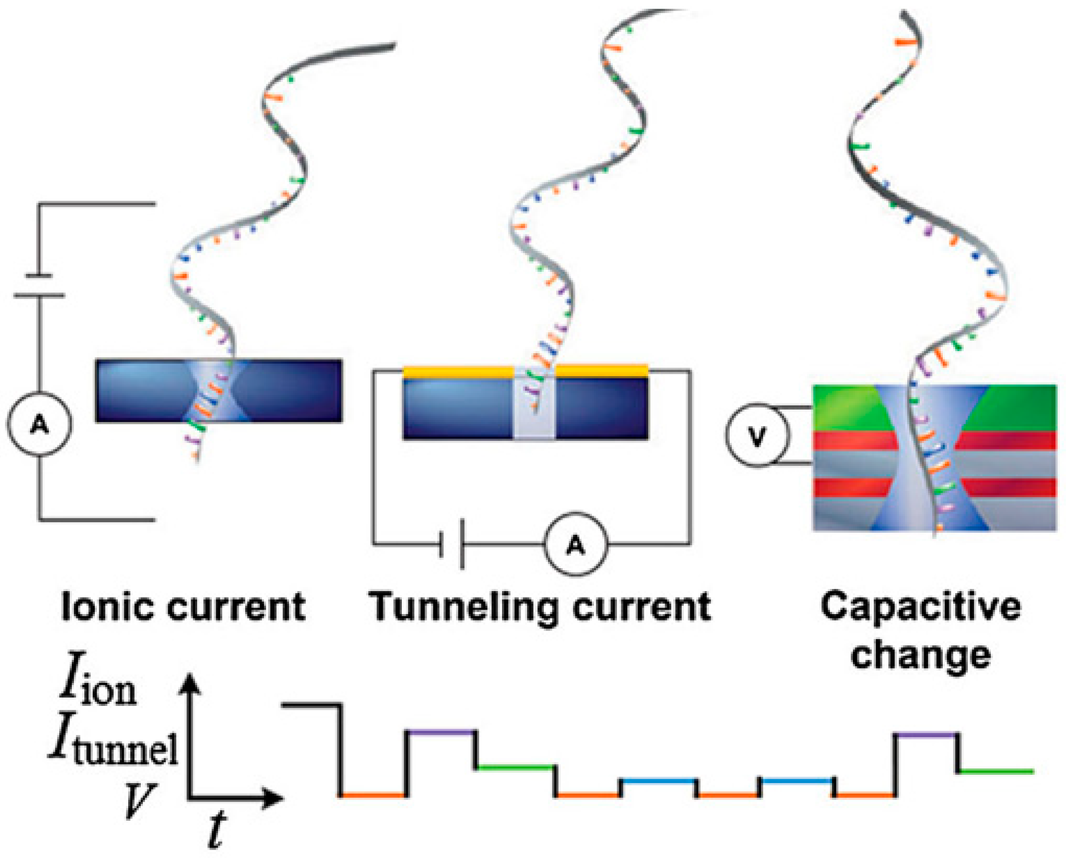
1. Introduction
2. Fabrication Strategies of Solid-State Nanopores
2.1. FIB and FEB Drilling Technology
2.2. Dielectric Breakdown Technology
2.3. Chemical Solution Etching Technologies
2.3.1. Feedback-Controlled Wet Etching
2.3.2. Ion-Track Etching

2.3.3. Electrochemical Anodization
2.3.4. Metal-Assisted Chemical Etching (MaCE)
2.4. EBL-Assisted Etching Technologies
2.5. Metal Deposition and Heating Method
2.6. Methods to Shrink Nanopores
2.6.1. FIB and FEB Induced Shrinkage Technology
2.6.2. Material Deposition Induced Shrinkage Technology
2.6.3. Thermal Oxidation Induced Shrinkage Technology
3. Applications
3.1. DNA Sequencing
3.2. Single Molecule Detection
3.3. Ion-Selective Transport
3.4. Nanopatterning
4. Challenges and Future Outlook
5. Conclusions
Author Contributions
Funding
Conflicts of Interest
References
- Kasianowicz, J.J.; Brandin, E.; Branton, D.; Deamer, D.W. Characterization of individual polynucleotide molecules using a membrane channel. Proc. Natl. Acad. Sci. USA 1996, 93, 13770–13773. [Google Scholar] [CrossRef]
- Feng, Y.; Zhang, Y.; Ying, C.; Wang, D.; Du, C. Nanopore-based Fourth-generation DNA Sequencing Technology. Genom. Proteom. Bioinform. 2015, 13, 4–16. [Google Scholar] [CrossRef] [PubMed]
- Venkatesan, B.M.; Bashir, R. Nanopore sensors for nucleic acid analysis. Nat. Nanotechnol. 2011, 6, 615–624. [Google Scholar] [CrossRef] [PubMed]
- Miles, B.N.; Ivanov, A.P.; Wilson, K.A.; Doğan, F.; Japrung, D.; Edel, J.B. Single molecule sensing with solid-state nanopores: Novel materials, methods, and applications. Chem. Soc. Rev. 2012, 42, 15–28. [Google Scholar] [CrossRef]
- Clarke, J.; Wu, H.-C.; Jayasinghe, L.; Patel, A.; Reid, S.; Bayley, H. Continuous base identification for single-molecule nanopore DNA sequencing. Nat. Nanotechnol. 2009, 4, 265–270. [Google Scholar] [CrossRef] [PubMed]
- Nova, I.C.; Derrington, I.M.; Craig, J.M.; Noakes, M.T.; Tickman, B.I.; Doering, K.; Higinbotham, H.; Laszlo, A.H.; Gundlach, J.H. Investigating asymmetric salt profiles for nanopore DNA sequencing with biological porin MspA. PLoS ONE 2017, 12, e0181599. [Google Scholar] [CrossRef] [PubMed]
- Wendell, D.; Jing, P.; Geng, J.; Subramaniam, V.; Lee, T.J.; Montemagno, C.; Guo, P. Translocation of double-stranded DNA through membrane-adapted phi29 motor protein nanopores. Nat. Nanotechnol. 2009, 4, 765–772. [Google Scholar] [CrossRef]
- Japrung, D.; Henricus, M.; Li, Q.; Maglia, G.; Bayley, H. Urea Facilitates the Translocation of Single-Stranded DNA and RNA through the α-Hemolysin Nanopore. Biophys. J. 2010, 98, 1856–1863. [Google Scholar] [CrossRef] [PubMed]
- Haque, F.; Li, J.; Wu, H.-C.; Liang, X.-J.; Guo, P. Solid-state and biological nanopore for real-time sensing of single chemical and sequencing of DNA. Nano Today 2013, 8, 56–74. [Google Scholar] [CrossRef]
- Fu, C.-y.; Prevelige, P.E. In vitro incorporation of the phage Phi29 connector complex. Virology 2009, 394, 149–153. [Google Scholar] [CrossRef] [PubMed]
- Guo, Y.Y.; Blocker, F.; Xiao, F.; Guo, P. Construction and 3-D computer modeling of connector arrays with tetragonal to decagonal transition induced by pRNA of phi29 DNA-packaging motor. J. Nanosci. Nanotechnol. 2005, 5, 856–863. [Google Scholar] [CrossRef][Green Version]
- Ji, Z.; Kang, X.; Wang, S.; Guo, P. Nano-channel of viral DNA packaging motor as single pore to differentiate peptides with single amino acid difference. Biomaterials 2018, 182, 227–233. [Google Scholar] [CrossRef]
- Majd, S.; Yusko, E.C.; Billeh, Y.N.; Macrae, M.X.; Yang, J.; Mayer, M. Applications of biological pores in nanomedicine, sensing, and nanoelectronics. Curr. Opin. Biotechnol. 2010, 21, 439–476. [Google Scholar] [CrossRef]
- Stranges, P.B.; Palla, M.; Kalachikov, S.; Nivala, J.; Dorwart, M.; Trans, A.; Kumar, S.; Porel, M.; Chien, M.; Tao, C. Design and characterization of a nanopore-coupled polymerase for single-molecule DNA sequencing by synthesis on an electrode array. Proc. Natl. Acad. Sci. USA 2016, 113, E6749–E6756. [Google Scholar] [CrossRef] [PubMed]
- Fuller, C.W.; Kumar, S.; Porel, M.; Chien, M.; Bibillo, A.; Stranges, P.B.; Dorwart, M.; Tao, C.; Li, Z.; Guo, W. Real-time single-molecule electronic DNA sequencing by synthesis using polymer-tagged nucleotides on a nanopore array. Proc. Natl. Acad. Sci. USA 2016, 113, 5233–5238. [Google Scholar] [CrossRef] [PubMed]
- Storm, A.J.; Chen, J.H.; Ling, X.S.; Zandbergen, H.W.; Dekker, C. Fabrication of solid-state nanopores with single-nanometre precision. Nat. Mater. 2003, 2, 537–540. [Google Scholar] [CrossRef]
- Li, J.; Gershow, M.; Stein, D.; Brandin, E.; Golovchenko, J.A. DNA molecules and configurations in a solid-state nanoporemicroscope. Nat. Mater. 2003, 2, 611–615. [Google Scholar] [CrossRef] [PubMed]
- Heng, J.B.; Ho, C.; Kim, T.; Timp, R.; Aksimentiev, A.; Grinkova, Y.V.; Sligar, S.; Schulten, K.; Timp, G. Sizing DNA using a nanometer-diameter pore. Biophys. J. 2004, 87, 2905–2911. [Google Scholar] [CrossRef] [PubMed]
- Heng, J.B.; Aksimentiev, A.; Ho, C.; Marks, P.; Grinkova, Y.V.; Sligar, S.; Schulten, K.; Timp, G. Stretching DNA using the electric field in a synthetic nanopore. Nano Lett. 2005, 5, 1883–1888. [Google Scholar] [CrossRef] [PubMed]
- Heng, J.B.; Aksimentiev, A.; Ho, C.; Marks, P.; Grinkova, Y.V.; Sligar, S.; Schulten, K.; Timp, G. The Electromechanics of DNA in a Synthetic Nanopore. Biophys. J. 2006, 90, 1098–1106. [Google Scholar] [CrossRef]
- Dekker, C. Solid-state nanopores. Nat. Nanotechnol. 2007, 2, 209–215. [Google Scholar] [CrossRef]
- Deng, T.; Li, M.; Wang, Y.; Liu, Z. Development of solid-state nanopore fabrication technologies. Sci. Bull. 2015, 60, 304–319. [Google Scholar] [CrossRef]
- Storm, A.J.; Chen, J.H.; Zandbergen, H.W.; Dekker, C. Translocation of double-strand DNA through a silicon oxide nanopore. Phys. Rev. E 2005, 71, 051903. [Google Scholar] [CrossRef]
- Larkin, J.; Henley, R.; Bell, D.C.; Cohen-Karni, T.; Rosenstein, J.K.; Wanunu, M. Slow DNA transport through nanopores in hafnium oxide membranes. ACS Nano 2013, 7, 10121–10128. [Google Scholar] [CrossRef] [PubMed]
- Fologea, D.; Gershow, M.; Ledden, B.; Mcnabb, D.S.; Golovchenko, J.A.; Li, J. Detecting Single Stranded DNA with a Solid State Nanopore. Nano Lett. 2005, 5, 1905–1909. [Google Scholar] [CrossRef]
- Griffiths, J. The Realm of the Nanopore. Analyt. Chem. 2008, 80, 23–27. [Google Scholar] [CrossRef]
- Xie, P.; Xiong, Q.; Fang, Y.; Quan, Q.; Lieber, C.M. Local electrical potential detection of DNA by nanowire-nanopore sensors. Nat. Nanotechnol. 2012, 7, 119–125. [Google Scholar] [CrossRef]
- Niedringhaus, T.P.; Milanova, D.; Kerby, M.B.; Snyder, M.P.; Barron, A.E. Landscape of next-generation sequencing technologies. Anal. Chem. 2011, 83, 4327–4341. [Google Scholar] [CrossRef] [PubMed]
- Ohshiro, T.; Matsubara, K.; Tsutsui, M.; Furuhashi, M.; Taniguchi, M.; Kawai, T. Single-Molecule Electrical Random Resequencing of DNA and RNA. Sci. Rep. 2012, 2, 501. [Google Scholar] [CrossRef] [PubMed]
- Postma, H.W.C. Rapid Sequencing of Individual DNA Molecules in Graphene Nanogaps. Nano Lett. 2010, 10, 420–425. [Google Scholar] [CrossRef]
- Tsutsui, M.; Taniguchi, M.; Yokota, K.; Kawai, T. Identifying single nucleotides by tunnelling current. Nat. Nanotechnol. 2010, 5, 286–290. [Google Scholar] [CrossRef] [PubMed]
- Sigalov, G.; Comer, J.; Timp, G.; Aksimentiev, A. Detection of DNA sequences using an alternating electric field in a nanopore capacitor. Nano Lett. 2008, 8, 56–63. [Google Scholar] [CrossRef] [PubMed]
- Gracheva, M.E.; Aksimentiev, A.; Leburton, J.P. Electrical signatures of single-stranded DNA with single base mutations in a nanopore capacitor. Nanotechnology 2015, 17, 3160. [Google Scholar] [CrossRef]
- Yokota, K.; Tsutsui, M.; Taniguchi, M. Electrode-embedded nanopores for label-free single-molecule sequencing by electric currents. RSC Adv. 2014, 4, 15886–15899. [Google Scholar] [CrossRef]
- O’Hern, S.C.; Jang, D.; Bose, S.; Idrobo, J.-C.; Song, Y.; Laoui, T.; Kong, J.; Karnik, R. Nanofiltration across Defect-Sealed Nanoporous Monolayer Graphene. Nano Lett. 2015, 15, 3254–3260. [Google Scholar] [CrossRef]
- Wu, K.; Chen, Z.; Li, X. Real gas transport through nanopores of varying cross-section type and shape in shale gas reservoirs. Chem. Eng. J. 2015, 281, 813–825. [Google Scholar] [CrossRef]
- Feng, J.; Graf, M.; Liu, K.; Ovchinnikov, D.; Dumcenco, D.; Heiranian, M.; Nandigana, V.; Aluru, N.R.; Kis, A.; Radenovic, A. Single-layer MoS2 nanopores as nanopower generators. Nature 2016, 536, 197–200. [Google Scholar] [CrossRef]
- Nandigana, V.V.R.; Jo, K.; Timperman, A.; Aluru, N.R. Asymmetric-Fluidic-Reservoirs Induced High Rectification Nanofluidic Diode. Sci. Rep. 2018, 8. [Google Scholar] [CrossRef]
- Yuan, Z.; Wang, C.; Yi, X.; Ni, Z.; Chen, Y.; Li, T. Solid-State Nanopore. Nanoscale Res. Lett. 2018, 13, 56. [Google Scholar] [CrossRef]
- Kudr, J.; Skalickova, S.; Nejdl, L.; Moulick, A.; Ruttkay-Nedecky, B.; Adam, V.; Kizek, R. Fabrication of solid-state nanopores and its perspectives. Electrophoresis 2015, 36, 2367–2379. [Google Scholar] [CrossRef]
- Tang, Z.; Zhang, D.; Cui, W.; Hao, Z.; Wei, P.; Duan, X. Fabrications, Applications and Challenges of Solid-State Nanopores: A Mini Review. Nanomater. Nanotechnol. 2016, 6, 35. [Google Scholar] [CrossRef][Green Version]
- Kim, M.J.; Mcnally, B.; Murata, K.; Meller, A. Characteristics of solid-state nanometre pores fabricated using a transmission electron microscope. Nanotechnology 2007, 18, 7554–7560. [Google Scholar] [CrossRef]
- Lin, Y.; Ying, Y.L.; Shi, X.; Liu, S.C.; Long, Y.T. Direct sensing of cancer biomarkers in clinical samples with a designed nanopore. Chem. Commun. 2017, 53, 11564–11567. [Google Scholar] [CrossRef]
- Krapf, D.; Wu, M.Y.; Smeets, R.M.; Zandbergen, H.W.; Dekker, C.; Lemay, S.G. Fabrication and characterization of nanopore-based electrodes with radii down to 2 nm. Nano Lett. 2006, 6, 105–109. [Google Scholar] [CrossRef]
- Lo, C.J.; Aref, T.; Bezryadin, A. Fabrication of symmetric sub-5 nm nanopores using focused ion and electron beams. Nanotechnology 2006, 17, 3264–3267. [Google Scholar] [CrossRef]
- Gierak, J.; Madouri, A.; Biance, A.L.; Bourhis, E.; Patriarche, G.; Ulysse, C.; Lucot, D.; Lafosse, X.; Auvray, L.; Bruchhaus, L. Sub-5nm FIB direct patterning of nanodevices. Microelectron. Eng. 2007, 84, 779–783. [Google Scholar] [CrossRef]
- Wu, S.; Cao, F.; Zheng, H.; Sheng, H.; Liu, C.; Liu, Y.; Zhao, D.; Wang, J. Fabrication of faceted nanopores in magnesium. Appl. Phys. Lett. 2013, 103, 243101. [Google Scholar] [CrossRef]
- Morin, A.; Lucot, D.; Ouerghi, A.; Patriarche, G.; Bourhis, E.; Madouri, A.; Ulysse, C.; Pelta, J.; Bruchhaus, L.; Bruchhaus, L. FIB carving of nanopores into suspended graphene films. Microelectron. Eng. 2012, 97, 311–316. [Google Scholar] [CrossRef]
- Patterson, N.; Adams, D.P.; Hodges, V.C.; Vasile, M.J.; Michael, J.R.; Kotula, P.G. Controlled fabrication of nanopores using a direct focused ion beam approach with back face particle detection. Nanotechnology 2008, 19, 235304. [Google Scholar] [CrossRef]
- Marshall, M.M.; Yang, J.; Hall, A.R. Direct and Transmission Milling of Suspended Silicon Nitride Membranes With a Focused Helium Ion Beam. Scanning 2012, 34, 101–106. [Google Scholar] [CrossRef]
- Hemamouche, A.; Morin, A.; Bourhis, E.; Toury, B.; Tarnaud, E.; Madouri, A.; Lafosse, X.; Ulysse, C.; Guilet, S.; Patriarche, G. FIB patterning of dielectric, metallized and graphene membranes: A comparative study. Microelectron. Eng. 2014, 121, 87–91. [Google Scholar] [CrossRef]
- Li, J.; Stein, D.; McMullan, C.; Branton, D.; Aziz, M.J.; Golovchenko, J.A. Ion-beam sculpting at nanometre length scales. Nature 2001, 412, 166–169. [Google Scholar] [CrossRef] [PubMed]
- Gierak, J.; Mailly, D.; Hawkes, P.; Jede, R.; Bruchhaus, L.; Bardotti, L.; Prével, B.; Mélinon, P.; Perez, A.; Hyndman, R. Exploration of the ultimate patterning potential achievable with high resolution focused ion beams. Appl. Phys. A 2005, 80, 187–194. [Google Scholar] [CrossRef]
- Emmrich, D.; Beyer, A.; Nadzeyka, A.; Bauerdick, S.; Meyer, J.C.; Kotakoski, J.; Goelzhaeuser, A. Nanopore fabrication and characterization by helium ion microscopy. Appl. Phys. Lett. 2016, 108. [Google Scholar] [CrossRef]
- Shim, J.; Rivera, J.A.; Bashir, R. Electron beam induced local crystallization of HfO2 nanopores for biosensing applications. Nanoscale 2013, 5, 10887–10893. [Google Scholar] [CrossRef] [PubMed]
- Traversi, F.; Raillon, C.; Benameur, S.M.; Liu, K.; Khlybov, S.; Tosun, M.; Krasnozhon, D.; Kis, A.; Radenovic, A. Detecting the translocation of DNA through a nanopore using graphene nanoribbons. Nat. Nanotechnol. 2013, 8, 939–945. [Google Scholar] [CrossRef] [PubMed]
- Liu, S.; Lu, B.; Zhao, Q.; Li, J.; Gao, T.; Chen, Y.; Zhang, Y.; Liu, Z.; Fan, Z.; Yang, F. Boron Nitride Nanopores: Highly Sensitive DNA Single-Molecule Detectors. Adv. Mater. 2013, 25, 4549–4554. [Google Scholar] [CrossRef]
- Liu, K.K.; Zhang, W.; Lee, Y.H.; Lin, Y.C.; Chang, M.T.; Su, C.Y.; Chang, C.S.; Li, H.; Shi, Y.; Zhang, H. Growth of Large-Area and Highly Crystalline MoS2 Thin Layers on Insulating Substrates. Nano Lett. 2012, 12, 1538–1544. [Google Scholar] [CrossRef]
- Kwok, H.; Briggs, K.; Tabardcossa, V. Nanopore Fabrication by Controlled Dielectric Breakdown. PLoS ONE 2014, 9, e92880. [Google Scholar] [CrossRef]
- Yanagi, I.; Akahori, R.; Hatano, T.; Takeda, K.-i. Fabricating nanopores with diameters of sub-1 nm to 3 nm using multilevel pulse-voltage injection. Sci. Rep. 2014, 4, 5000. [Google Scholar] [CrossRef]
- Ying, C.; Houghtaling, J.; Eggenberger, O.M.; Guha, A.; Nirmalraj, P.; Awasthi, S.; Tian, J.; Mayer, M. Formation of Single Nanopores with Diameters of 20–50 nm in Silicon Nitride Membranes Using Laser-Assisted Controlled Breakdown. ACS Nano 2018, 12, 11458–11470. [Google Scholar] [CrossRef] [PubMed]
- Yamazaki, H.; Hu, R.; Zhao, Q.; Wanunu, M. Photothermally Assisted Thinning of Silicon Nitride Membranes for Ultrathin Asymmetric Nanopores. ACS Nano 2018, 12, 12472–12481. [Google Scholar] [CrossRef]
- Wang, Y.; Chen, Q.; Deng, T.; Liu, Z. Self-Aligned Nanopore Formed on a SiO2 Pyramidal Membrane by a Multipulse Dielectric Breakdown Method. J. Phys. Chem. C 2018, 122, 11516–11523. [Google Scholar] [CrossRef]
- Wang, Y.; Chen, Q.; Deng, T.; Liu, Z. Nanopore fabricated in pyramidal HfO2 film by dielectric breakdown method. Appl. Phys. Lett. 2017, 111, 143103. [Google Scholar] [CrossRef]
- Park, S.R.; Peng, H.; Ling, X.S. Fabrication of nanopores in silicon chips using feedback chemical etching. Small 2007, 3, 116–119. [Google Scholar] [CrossRef]
- Chen, Q.; Wang, Y.; Deng, T.; Liu, Z. Fabrication of Nanopores and Nanoslits with Feature Sizes Down to 5 nm by Wet Etching Method. Nanotechnology 2018, 29, 085301. [Google Scholar] [CrossRef] [PubMed]
- Siwy, Z.; Dobrev, D.; Neumann, R.; Trautmann, C.; Voss, K. Electro-responsive asymmetric nanopores in polyimide with stable ion-current signal. Appl. Phys. A 2003, 76, 781–785. [Google Scholar] [CrossRef]
- Harrell, C.C.; Choi, Y.; Horne, L.P.; Baker, L.A.; Siwy, Z.S.; Martin, C.R. Resistive-Pulse DNA Detection with a Conical Nanopore Sensor. Langmuir 2006, 22, 10837–10843. [Google Scholar] [CrossRef] [PubMed]
- Apel, P.Y.; Korchev, Y.E.; Siwy, Z.; Spohr, R.; Yoshida, M. Diode-like single-ion track membrane prepared by electro-stopping. Nucl. Instrum. Methods Phys. Res. Sect. B 2001, 184, 337–346. [Google Scholar] [CrossRef]
- Yuan, J.H.; He, F.Y.; And, D.C.S.; Xia, X.H. A Simple Method for Preparation of Through-Hole Porous Anodic Alumina Membrane. Chem. Mater. 2004, 16, 1841–1844. [Google Scholar] [CrossRef]
- Lee, W.; Ji, R.; Gösele, U.; Nielsch, K. Fast fabrication of long-range ordered porous alumina membranes by hard anodization. Nat. Mater. 2006, 5, 741–747. [Google Scholar] [CrossRef]
- Masuda, H.; Fukuda, K. Ordered Metal Nanohole Arrays Made by a Two-Step Replication of Honeycomb Structures of Anodic Alumina. Science 1995, 268, 1466–1468. [Google Scholar] [CrossRef] [PubMed]
- Sulka, G.D.; Kapusta-Kołodziej, J.; Brzózka, A.; Jaskuła, M. Anodic growth of TiO2 nanopore arrays at various temperatures. Electrochim. Acta 2013, 104, 526–535. [Google Scholar] [CrossRef]
- Huang, Z.; Geyer, N.; Werner, P.; De Boor, J.; Gösele, U. Metal-Assisted Chemical Etching of Silicon: A Review. Adv. Mater. 2011, 23, 285–308. [Google Scholar] [CrossRef]
- Hildreth, O.J.; Brown, D.; Wong, C.P. 3D Out-of-Plane Rotational Etching with Pinned Catalysts in Metal-Assisted Chemical Etching of Silicon. Adv. Funct. Mater. 2011, 21, 3119–3128. [Google Scholar] [CrossRef]
- Tsujino, K.; Matsumura, M. Boring Deep Cylindrical Nanoholes in Silicon Using Silver Nanoparticles as a Catalyst. Adv. Mater. 2005, 36, 1045–1047. [Google Scholar] [CrossRef]
- Dimova-Malinovska, D.; Sendova-Vassileva, M.; Tzenov, N.; Kamenova, M. Preparation of thin porous silicon layers by stain etching. Thin Solid Films 1997, 297, 9–12. [Google Scholar] [CrossRef]
- Tao, D. Massive fabrication of silicon nanopore arrays with tunable shapes. Appl. Surf. Sci. 2016, 390, 681–688. [Google Scholar]
- Yameen, B.; Ali, M.; Neumann, R.; Ensinger, W.; Knoll, W.; Azzaroni, O. Single Conical Nanopores Displaying pH-Tunable Rectifying Characteristics. Manipulating Ionic Transport with Zwitterionic Polymer Brushes. J. Am. Chem. Soc. 2009, 131, 2070–2071. [Google Scholar] [CrossRef]
- Siwy, Z.S. Ion-current rectification in nanopores and nanotubes with broken symmetry. Adv. Funct. Mater. 2006, 16, 735–746. [Google Scholar] [CrossRef]
- Lin, C.-Y.; Yeh, L.-H.; Siwy, Z.S. Voltage-Induced Modulation of Ionic Concentrations and Ion Current Rectification in Mesopores with Highly Charged Pore Walls. J. Phys. Chem. Lett. 2018, 9, 393–398. [Google Scholar] [CrossRef]
- Apel, P.Y.; Blonskaya, I.V.; Dmitriev, S.N.; Orelovitch, O.L.; Presz, A.; Sartowska, B.A. Fabrication of nanopores in polymer foils with surfactant-controlled longitudinal profiles. Nanotechnology 2007, 18, 305302. [Google Scholar] [CrossRef]
- Siwy, Z.; Fulinski, A. Fabrication of a synthetic nanopore ion pump. Phys. Rev. Lett. 2002, 89, 198103. [Google Scholar] [CrossRef] [PubMed]
- Tsujino, K.; Matsumura, M. Morphology of nanoholes formed in silicon by wet etching in solutions containing HF and H2O2 at different concentrations using silver nanoparticles as catalysts. Electrochim. Acta 2007, 53, 28–34. [Google Scholar] [CrossRef]
- Han, A.; Schürmann, G.; Mondin, G.; Bitterli, R.A.; Hegelbach, N.G.; Rooij, N.F.D.; Staufer, U. Sensing protein molecules using nanofabricated pores. Appl. Phys. Lett. 2006, 88, 093901. [Google Scholar] [CrossRef]
- Feng, Y.; Wang, D.; Bai, J.; Nam, S.W.; Peng, H.; Bruce, R.; Gignac, L.; Brink, M.; Waggoner, P.; Wang, C. Fabrication of Sub-20 NM Nanopore Arrays in Membranes with Embedded Metal Electrodes at Wafer Scales. Nanoscale 2014, 6, 8900–8906. [Google Scholar] [CrossRef][Green Version]
- Guo, L.J. Nanoimprint lithography: Methods and material requirements. Adv. Mater. 2007, 19, 495–513. [Google Scholar] [CrossRef]
- Chou, S.Y.; Krauss, P.R.; Zhang, W.; Guo, L.; Zhuang, L. Sub-10 nm imprint lithography and applications. J. Vac. Sci. Technol. B Microelectron. Nanometer Struct. Process. Meas. Phenom. 1997, 15, 2897–2904. [Google Scholar] [CrossRef]
- Kustandi, T.S.; Loh, W.W.; Gao, H.; Low, H.Y. Wafer-Scale Near-Perfect Ordered Porous Alumina on Substrates by Step and Flash Imprint Lithography. ACS Nano 2010, 4, 2561–2568. [Google Scholar] [CrossRef]
- Vreede, L.J.D.; Muniz, M.S.; Berg, A.V.D.; Eijkel, J.C.T. Nanopore fabrication in silicon oxynitride membranes by heating Au-particles. J. Micromechan. Microeng. 2016, 26, 037001. [Google Scholar] [CrossRef]
- De Vreede, L.J. Nanopore Fabrication by Heating Au particles on Ceramic Substrates. Nano Lett. 2015, 15, 727–731. [Google Scholar] [CrossRef]
- Park, T.; Lee, S.J.; Cha, J.H.; Choi, W. Scalable fabrication of nanopores in membranes via thermal annealing of Au nanoparticles. Nanoscale 2018, 10, 22623–22634. [Google Scholar] [CrossRef] [PubMed]
- Saiz, E.; Tomsia, A.P.; Cannon, R.M. Ridging effects on wetting and spreading of liquids on solids. Acta Mater. 1998, 46, 2349–2361. [Google Scholar] [CrossRef]
- Ghetta, V.; Chatain, D. Morphologies Adopted by Al2O3 Single-Crystal Surfaces in Contact with Cu Droplets. J. Am. Ceram. Soc. 2010, 85, 961–964. [Google Scholar] [CrossRef]
- Shi, L.; Shen, P.; Zhang, D.; Jiang, Q. Pinning–depinning behavior in the wetting of (0001) α-Al2O3 single crystal by molten Mg. Appl. Surf. Sci. 2011, 257, 10743–10747. [Google Scholar] [CrossRef]
- Zhang, W.M.; Wang, Y.G.; Li, J.; Xue, J.M.; Ji, H.; Ouyang, Q.; Xu, J.; Zhang, Y. Controllable shrinking and shaping of silicon nitride nanopores under electron irradiation. Appl. Phys. Lett. 2007, 90. [Google Scholar] [CrossRef]
- Zheng, H.; Liu, Y.; Cao, F.; Wu, S.; Jia, S.; Cao, A.; Zhao, D.; Wang, J. Electron beam-assisted healing of nanopores in magnesium alloys. Sci. Rep. 2013, 3, 1920. [Google Scholar] [CrossRef] [PubMed]
- Chen, Q.; Wang, Y.F.; Deng, T.; Liu, Z.W. SEM-induced shrinkage and site-selective modification of single-crystal silicon nanopores. Nanotechnology 2017, 28, 305301. [Google Scholar] [CrossRef]
- Kox, R.; Chen, C.; Maes, G.; Lagae, L.; Borghs, G. Shrinking solid-state nanopores using electron-beam-induced deposition. Nanotechnology 2009, 20, 115302. [Google Scholar] [CrossRef]
- Danelon, C.; Santschi, C.; Brugger, J.; Vogel, H. Fabrication and functionalization of nanochannels by electron-beam-induced silicon oxide deposition. Langmuir 2006, 22, 10711–10715. [Google Scholar] [CrossRef]
- Chang, H.; Iqbal, S.M.; Stach, E.A.; King, A.H.; Zaluzec, N.J.; Bashir, R. Fabrication and characterization of solid-state nanopores using a field emission scanning electron microscope. Appl. Phys. Lett. 2006, 88. [Google Scholar] [CrossRef]
- Chen, Q.; Wang, Y.; Liu, Z. Fabrication of silicon nanopores with tunable shapes and sizes. In Proceedings of the 2018 China Semiconductor Technology International Conference (CSTIC), Shanghai, China, 11–12 March 2018; pp. 1–3. [Google Scholar]
- Chen, P.; Mitsui, T.; Farmer, D.B.; Golovchenko, J.; Gordon, R.G.; Branton, D. Atomic Layer Deposition to Fine-Tune the Surface Properties and Diameters of Fabricated Nanopores. Nano Lett. 2004, 4, 1333–1337. [Google Scholar] [CrossRef]
- Nilsson, J.; Lee, J.R.I.; Ratto, T.V.; Létant, S.E. Localized Functionalization of Single Nanopores. Adv. Mater. 2010, 18, 427–431. [Google Scholar] [CrossRef]
- Ayub, M.; Ivanov, A.; Hong, J.; Kuhn, P.; Instuli, E.; Edel, J.B.; Albrecht, T. Precise electrochemical fabrication of sub-20 nm solid-state nanopores for single-molecule biosensing. J. Phys. Condens. Matter. 2010, 22, 454128. [Google Scholar] [CrossRef]
- Wang, Y.; Deng, T.; Chen, Q.; Liang, F.; Liu, Z. Highly efficient shrinkage of inverted-pyramid silicon nanopores by plasma-enhanced chemical vapor deposition technology. Nanotechnology 2016, 27, 254005. [Google Scholar] [CrossRef]
- Asghar, W.; Ilyas, A.; Billo, J.A.; Iqbal, S.M. Shrinking of Solid-state Nanopores by Direct Thermal Heating. Nanoscale Res. Lett. 2011, 6, 372. [Google Scholar] [CrossRef]
- Deng, T.; Chen, J.; Li, M.; Wang, Y.; Zhao, C.; Zhang, Z.; Liu, Z. Controllable shrinking of inverted-pyramid silicon nanopore arrays by dry-oxygen oxidation. Nanotechnology 2013, 24, 505303. [Google Scholar] [CrossRef] [PubMed]
- Prabhu, A.S.; Freedman, K.J.; Robertson, J.W.; Nikolov, Z.; Kasianowicz, J.J.; Kim, M.J. SEM-induced shrinking of solid-state nanopores for single molecule detection. Nanotechnology 2011, 22, 425302. [Google Scholar] [CrossRef] [PubMed]
- Venkatesan, B.M.; Dorvel, B.; Yemenicioglu, S.; Watkins, N.; Petrov, I.; Bashir, R. Highly Sensitive, Mechanically Stable Nanopore Sensors for DNA Analysis. Adv. Mater. 2010, 21, 2771–2776. [Google Scholar] [CrossRef]
- Feng, J.; Liu, K.; Graf, M.; Lihter, M.; Bulushev, R.; Dumcenco, D.; Alexander, D.; Krasnozhon, D.; Kis, A.; Radenovic, A. Electrochemical reaction in single layer MoS2: Nanopores opened atom by atom. Nano Lett. 2015, 15, 3431–3438. [Google Scholar] [CrossRef]
- Garaj, S.; Hubbard, W.; Reina, A.; Kong, J.; Branton, D.; Golovchenko, J.A. Graphene as a subnanometre trans-electrode membrane. Nature 2010, 467, 190–193. [Google Scholar] [CrossRef] [PubMed]
- Zhou, Z.; Hu, Y.; Wang, H.; Xu, Z.; Wang, W.; Bai, X.; Shan, X.; Lu, X. DNA Translocation through Hydrophilic Nanopore in Hexagonal Boron Nitride. Sci. Rep. 2013, 3, 3287. [Google Scholar] [CrossRef] [PubMed]
- Park, K.B.; Kim, H.J.; Kim, H.M.; Han, S.A.; Lee, K.H.; Kim, S.W.; Kim, K.B. Noise and sensitivity characteristics of solid-state nanopores with a boron nitride 2-D membrane on a pyrex substrate. Nanoscale 2016, 8, 5755–5763. [Google Scholar] [CrossRef]
- Yanagi, I.; Akahori, R.; Yokoi, T.; Takeda, K.-I. Precise Fabrication of Nanopores with Diameters of Sub-1 nm to 3 nm Using Multilevel Pulse-voltage Injection. Sci. Rep. 2014, 4, 5000. [Google Scholar] [CrossRef] [PubMed]
- Han, A.; Creus, M.; Schürmann, G.; Linder, V.; Ward, T.R.; de Rooij, N.F.; Staufer, U. Label-free detection of single protein molecules and protein-protein interactions using synthetic nanopores. Anal. Chem. 2008, 80, 4651–4658. [Google Scholar] [CrossRef] [PubMed]
- Venta, K.; Shemer, G.; Puster, M.; Rodríguez-Manzo, J.A.; Balan, A.; Rosenstein, J.K.; Shepard, K.; Drndić, M. Differentiation of Short, Single-Stranded DNA Homopolymers in Solid-State Nanopores. ACS Nano 2013, 7, 4629–4636. [Google Scholar] [CrossRef]
- Lee, M.H.; Kumar, A.; Park, K.B.; Cho, S.Y.; Kim, H.M.; Lim, M.C.; Kim, Y.R.; Kim, K.B. A low-noise solid-state nanopore platform based on a highly insulating substrate. Sci. Rep. 2014, 4, 7448. [Google Scholar] [CrossRef]
- Feng, J.; Liu, K.; Bulushev, R.D.; Khlybov, S.; Dumcenco, D.; Kis, A.; Radenovic, A. Identification of single nucleotides in MoS2 nanopores. Nat. Nanotechnol. 2015, 10, 1070–1076. [Google Scholar] [CrossRef]
- Branton, D.; Deamer, D.W.; Marziali, A.; Bayley, H.; Benner, S.A.; Butler, T.; Di, V.M.; Garaj, S.; Hibbs, A.; Huang, X. The potential and challenges of nanopore sequencing. Nat. Biotechnol. 2008, 26, 1146–1153. [Google Scholar] [CrossRef]
- Storm, A.J.; Storm, C.; Chen, J.; Zandbergen, H.; Joanny, J.F.; Dekker, C. Fast DNA translocation through a solid-state nanopore. Nano Lett. 2005, 5, 1193–1197. [Google Scholar] [CrossRef]
- Chen, Z.; Jiang, Y.; Dunphy, D.R.; Adams, D.P.; Hodges, C.; Liu, N.; Zhang, N.; Xomeritakis, G.; Jin, X.; Aluru, N.R.; et al. DNA translocation through an array of kinked nanopores. Nat. Mater. 2010, 9, 667–675. [Google Scholar] [CrossRef]
- Schneider, G.F.; Xu, Q.; Hage, S.; Luik, S.; Spoor, J.N.; Malladi, S.; Zandbergen, H.; Dekker, C. Tailoring the hydrophobicity of graphene for its use as nanopores for DNA translocation. Nat. Commun. 2013, 4, 2619. [Google Scholar] [CrossRef]
- Tang, Z.; Lu, B.; Zhao, Q.; Wang, J.; Luo, K.; Yu, D. Surface modification of solid-state nanopores for sticky-free translocation of single-stranded DNA. Small 2014, 10, 4332–4339. [Google Scholar] [CrossRef]
- Nakane, J.; Wiggin, M.; Marziali, A. A Nanosensor for Transmembrane Capture and Identification of Single Nucleic Acid Molecules. Biophys. J. 2004, 87, 615–621. [Google Scholar] [CrossRef]
- Tropini, C.; Marziali, A. Multi-Nanopore Force Spectroscopy for DNA Analysis. Biophys. J. 2007, 92, 1632–1637. [Google Scholar] [CrossRef]
- Ji, L.; Yu, D.; Zhao, Q. Solid-state nanopore-based DNA single molecule detection and sequencing. Microchim. Acta 2016, 183, 941–953. [Google Scholar]
- Lee, K.; Park, K.-B.; Kim, H.-J.; Yu, J.-S.; Chae, H.; Kim, H.-M.; Kim, K.-B. Recent Progress in Solid-State Nanopores. Adv. Mater. 2018, 30, 1704680. [Google Scholar] [CrossRef]
- Wasfi, A.; Awwad, F.; Ayesh, A.I. Graphene-based nanopore approaches for DNA sequencing: A literature review. Biosens. Bioelectron. 2018, 119, 191–203. [Google Scholar] [CrossRef]
- Liu, Z.; Wang, Y.; Deng, T.; Chen, Q. Solid-State Nanopore-Based DNA Sequencing Technology. J. Nanomater. 2016, 2016, 5284786. [Google Scholar] [CrossRef]
- Merchant, C.A.; Healy, K.; Wanunu, M.; Ray, V.; Peterman, N.; Bartel, J.; Fischbein, M.D.; Venta, K.; Luo, Z.; Johnson, A.T.C.; et al. DNA Translocation through Graphene Nanopores. Nano Lett. 2010, 10, 2915–2921. [Google Scholar] [CrossRef]
- Liu, K.; Feng, J.; Kis, A.; Radenovic, A. Atomically thin molybdenum disulfide nanopores with high sensitivity for DNA translocation. ACS Nano 2014, 8, 2504–2511. [Google Scholar] [CrossRef]
- Wanunu, M.; Morrison, W.; Rabin, Y.; Grosberg, A.Y.; Meller, A. Electrostatic focusing of unlabelled DNA into nanoscale pores using a salt gradient. Nat. Nanotechnol. 2010, 5, 160–165. [Google Scholar] [CrossRef]
- Wanunu, M.; Dadosh, T.; Ray, V.; Jin, J.; Mcreynolds, L.; Drndić, M. Rapid electronic detection of probe-specific microRNAs using thin nanopore sensors. Nat. Nanotechnol. 2010, 5, 807–814. [Google Scholar] [CrossRef]
- Keyser, U.F.; van der Does, J.; Dekker, C.; Dekker, N.H. Optical tweezers for force measurements on DNA in nanopores. Rev. Sci. Instrum. 2006, 77, 105105. [Google Scholar] [CrossRef]
- Dorp, S.V.; Keyser, U.F.; Dekker, N.H.; Dekker, C.; Lemay, S.G. Origin of the electrophoretic force on DNA in solid-state nanopores. Nat. Phys. 2009, 5, 347–351. [Google Scholar] [CrossRef]
- Peng, H.; Ling, X.S. Reverse DNA translocation through a solid-state nanopore by magnetic tweezers. Nanotechnology 2009, 20, 185101. [Google Scholar] [CrossRef]
- Wanunu, M.; Sutin, J.; Mcnally, B.; Chow, A.; Meller, A. DNA translocation governed by interactions with solid-state nanopores. Biophys. J. 2008, 95, 4716–4725. [Google Scholar] [CrossRef]
- Luan, B.; Stolovitzky, G.; Martyna, G. Slowing and controlling the translocation of DNA in a solid-state nanopore. Nanoscale 2012, 4, 1068–1077. [Google Scholar] [CrossRef]
- Yusko, E.C.; Johnson, J.M.; Majd, S.; Prangkio, P.; Rollings, R.C.; Li, J.; Yang, J.; Mayer, M. Controlling protein translocation through nanopores with bio-inspired fluid walls. Nat. Nanotechnol. 2011, 6, 253–260. [Google Scholar] [CrossRef]
- Squires, A.H.; Hersey, J.S.; Grinstaff, M.W.; Meller, A. A nanopore-nanofiber mesh biosensor to control DNA translocation. J. Am. Chem. Soc. 2013, 135, 16304–16307. [Google Scholar] [CrossRef]
- Fologea, D.; Uplinger, J.; Thomas, B.; McNabb, D.S.; Li, J. Slowing DNA Translocation in a Solid-State Nanopore. Nano Lett. 2005, 5, 1734–1737. [Google Scholar] [CrossRef]
- Yeh, L.H.; Zhang, M.; Joo, S.W.; Qian, S. Slowing down DNA translocation through a nanopore by lowering fluid temperature. Electrophoresis 2012, 33, 3458–3465. [Google Scholar] [CrossRef] [PubMed]
- Smeets, R.M.; Keyser, U.F.; Krapf, D.; Wu, M.Y.; Dekker, N.H.; Dekker, C. Salt dependence of ion transport and DNA translocation through solid-state nanopores. Nano Lett. 2006, 6, 89–95. [Google Scholar] [CrossRef]
- Kowalczyk, S.W.; Wells, D.B.; Aksimentiev, A.; Dekker, C. Slowing down DNA Translocation through a Nanopore in Lithium Chloride. Nano Lett. 2012, 12, 1038–1044. [Google Scholar] [CrossRef]
- Tsutsui, M.; He, Y.; Furuhashi, M.; Rahong, S.; Taniguchi, M.; Kawai, T. Transverse electric field dragging of DNA in a nanochannel. Sci. Rep. 2012, 2, 394. [Google Scholar] [CrossRef]
- Lu, B.; Hoogerheide, D.P.; Zhao, Q.; Zhang, H.; Tang, Z.; Yu, D.; Golovchenko, J.A. Pressure-Controlled Motion of Single Polymers through Solid-State Nanopores. Nano Lett. 2013, 13, 3048–3052. [Google Scholar] [CrossRef]
- Zhang, H.; Zhao, Q.; Tang, Z.; Liu, S.; Li, Q.; Fan, Z.; Yang, F.; You, L.; Li, X.; Zhang, J. Slowing down DNA translocation through solid-state nanopores by pressure. Small 2013, 9, 4112–4117. [Google Scholar] [CrossRef]
- Hoogerheide, D.P.; Lu, B.; Golovchenko, J.A. Pressure-voltage trap for DNA near a solid-state nanopore. ACS Nano 2014, 8, 7384–7391. [Google Scholar] [CrossRef] [PubMed]
- Shendure, J.A.; Porreca, G.J.; Church, G.M.; Gardner, A.F.; Hendrickson, C.L.; Kieleczawa, J.; Slatko, B.E. Overview of DNA sequencing strategies. Curr. Protoc. Mol. Biol. 2011, 96, 7.1.1–7.1.23. [Google Scholar] [CrossRef]
- Qiu, H.; Sarathy, A.; Schulten, K.; Leburton, J.P. Detection and Mapping of DNA Methylation with 2D Material Nanopores. NPJ 2D Mater. Appl. 2017, 1, 3. [Google Scholar] [CrossRef]
- Shankla, M.; Aksimentiev, A. Conformational transitions and stop-and-go nanopore transport of single-stranded DNA on charged graphene. Nat. Commun. 2014, 5, 5171. [Google Scholar] [CrossRef]
- Wei, R.; Tampé, R.; Rant, U. Stochastic Sensing of Proteins with Receptor-Modified Solid-State Nanopores. Nat. Nanotechnol. 2012, 7, 257–263. [Google Scholar] [CrossRef]
- Larkin, J.; Henley, R.Y.; Muthukumar, M.; Rosenstein, J.K.; Wanunu, M. High-Bandwidth Protein Analysis Using Solid-State Nanopores. Biophys. J. 2014, 106, 696–704. [Google Scholar] [CrossRef] [PubMed]
- Venkatesan, B.M.; Estrada, D.; Banerjee, S.; Jin, X.; Dorgan, V.E.; Bae, M.H.; Aluru, N.R.; Pop, E.; Bashir, R. Stacked Graphene-Al2O3 Nanopore Sensors for Sensitive Detection of DNA and DNA–Protein Complexes. ACS Nano 2012, 6, 441–450. [Google Scholar] [CrossRef] [PubMed]
- Kowalczyk, S.W.; Hall, A.R.; Dekker, C. Detection of Local Protein Structures along DNA Using Solid-State Nanopores. Nano Lett. 2010, 10, 324–328. [Google Scholar] [CrossRef] [PubMed]
- Hall, A.R.; van Dorp, S.; Lemay, S.G.; Dekker, C. Electrophoretic Force on a Protein-Coated DNA Molecule in a Solid-State Nanopore. Nano Lett. 2009, 9, 4441–4445. [Google Scholar] [CrossRef] [PubMed]
- Marshall, M.M.; Jan, R.; Zahid, O.K.; Henrich, V.C.; Taylor, E.W.; Hall, A.R. Nanopore Analysis of Single-Stranded Binding Protein Interactions with DNA. Langmuir 2015, 31, 4582–4588. [Google Scholar] [CrossRef] [PubMed]
- Plesa, C.; Ruitenberg, J.W.; Witteveen, M.J.; Dekker, C. Detection of Individual Proteins Bound along DNA Using Solid-State Nanopores. Nano Lett. 2015, 15, 3153–3158. [Google Scholar] [CrossRef]
- Plesa, C.; Kowalczyk, S.W.; Zinsmeester, R.; Grosberg, A.Y.; Rabin, Y.; Dekker, C. Correction to Fast Translocation of Proteins through Solid State Nanopores. Nano Lett. 2013, 13, 3445. [Google Scholar] [CrossRef]
- Holden, D.A.; Hendrickson, G.; Lyon, L.A.; White, H.S. Resistive Pulse Analysis of Microgel Deformation During Nanopore Translocation. J. Phys. Chem. C 2011, 115, 2999–3004. [Google Scholar] [CrossRef]
- Lan, W.J.; Holden, D.A.; Zhang, B.; White, H.S. Nanoparticle transport in conical-shaped nanopores. Anal. Chem. 2011, 83, 3840–3847. [Google Scholar] [CrossRef]
- Schneider, G.F.; Kowalczyk, S.W.; Calado, V.E.; Pandraud, G.; Zandbergen, H.W.; Vandersypen, L.M.K.; Dekker, C. DNA Translocation through Graphene Nanopores. Nano Lett. 2010, 10, 3163–3167. [Google Scholar] [CrossRef] [PubMed]
- Rodríguezmanzo, J.A.; Puster, M.; Nicolaï, A.; Meunier, V.; Drndić, M. DNA Translocation in Nanometer Thick Silicon Nanopores. ACS Nano 2015, 9, 6555–6564. [Google Scholar] [CrossRef] [PubMed]
- Fologea, D.; Ledden, B.; McNabb, D.S.; Li, J. Electrical characterization of protein molecules by a solid-state nanopore. Appl. Phys. Lett. 2007, 91, 053901. [Google Scholar] [CrossRef] [PubMed]
- Steinbock, L.J.; Krishnan, S.; Bulushev, R.D.; Borgeaud, S.; Blokesch, M.; Feletti, L.; Radenovic, A. Probing the size of proteins with glass nanopores. Nanoscale 2014, 6, 14380–14387. [Google Scholar] [CrossRef]
- Li, W.; Bell, N.A.W.; Hernández-Ainsa, S.; Thacker, V.V.; Thackray, A.M.; Bujdoso, R.; Keyser, U.F. Single Protein Molecule Detection by Glass Nanopores. ACS Nano 2013, 7, 4129–4134. [Google Scholar] [CrossRef] [PubMed]
- Kubeil, C.; Bund, A. The Role of Nanopore Geometry for the Rectification of Ionic Currents. J. Phys. Chem. C 2011, 115, 7866–7873. [Google Scholar] [CrossRef]
- Cheng, L.-J.; Guo, L.J. Rectified Ion Transport through Concentration Gradient in Homogeneous Silica Nanochannels. Nano Lett. 2007, 7, 3165–3171. [Google Scholar] [CrossRef] [PubMed]
- Li, W.; Yang, Y.; Weber, J.K.; Zhang, G.; Zhou, R. Tunable, Strain-Controlled Nanoporous MoS2 Filter for Water Desalination. ACS Nano 2016, 10, 1829–1835. [Google Scholar] [CrossRef]
- Cohen-Tanugi, D.; Grossman, J.C. Water desalination across nanoporous graphene. Nano Lett. 2012, 12, 3602–3608. [Google Scholar] [CrossRef]
- Yanan, J.; Nannan, L.; Wei, G.; Fan, X.; Lei, J. Highly-efficient gating of solid-state nanochannels by DNA supersandwich structure containing ATP aptamers: A nanofluidic IMPLICATION logic device. J. Am. Chem. Soc. 2012, 134, 15395–15401. [Google Scholar]
- Nam, S.-W.; Rooks, M.J.; Kim, K.-B.; Rossnagel, S.M. Ionic Field Effect Transistors with Sub-10 nm Multiple Nanopores. Nano Lett. 2009, 9, 2044–2048. [Google Scholar] [CrossRef]
- Ramirez, P.; Gomez, V.; Cervera, J.; Nasir, S.; Ali, M.; Ensinger, W.; Mafe, S. Energy conversion from external fluctuating signals based on asymmetric nanopores. Nano Energy 2015, 16, 375–382. [Google Scholar] [CrossRef]
- Li, D.; Wei, H.; Zhang, J.; Hui, S.; Qu, C.; Sun, T.; Liang, L.; Qi, W. Separation of Hydrogen Gas from Coal Gas by Graphene Nanopore. J. Phys. Chem. C 2015, 119, 25559–25565. [Google Scholar] [CrossRef]
- Li, D.; Jing, W.; Li, S.; Shen, H.; Xing, W. Electric Field-Controlled Ion Transport In TiO2 Nanochannel. ACS Appl. Mater. Interfaces 2015, 7, 11294–11300. [Google Scholar] [CrossRef]
- He, Y.; Tsutsui, M.; Fan, C.; Taniguchi, M.; Kawai, T. Controlling DNA Translocation through Gate Modulation of Nanopore Wall Surface Charges. ACS Nano 2011, 5, 5509–5518. [Google Scholar] [CrossRef] [PubMed]
- Guo, W.; Cao, L.; Xia, J.; Nie, F.Q.; Ma, W.; Xue, J.; Song, Y.; Zhu, D.; Wang, Y.; Jiang, L. Energy Harvesting with Single-Ion-Selective Nanopores: A Concentration-Gradient-Driven Nanofluidic Power Source. Adv. Funct. Mater. 2010, 20, 1339–1344. [Google Scholar] [CrossRef]
- Lin, J.Y.; Lin, C.Y.; Hsu, J.P.; Tseng, S. Ionic Current Rectification in a pH-Tunable Polyelectrolyte Brushes Functionalized Conical Nanopore: Effect of Salt Gradient. Anal. Chem. 2015, 88, 1176–1187. [Google Scholar] [CrossRef]
- Ma, Y.; Yeh, L.-H.; Lin, C.-Y.; Mei, L.; Qian, S. pH-Regulated Ionic Conductance in a Nanochannel with Overlapped Electric Double Layers. Anal. Chem. 2015, 87, 4508–4514. [Google Scholar] [CrossRef]
- Wu, M.; Wen, L.; Lei, Y.; Ostendorp, S.; Chen, K.; Wilde, G. Ultrathin Alumina Membranes for Surface Nanopatterning in Fabricating Quantum-Sized Nanodots. Small 2010, 6, 695–699. [Google Scholar] [CrossRef] [PubMed]
- Tan, L.K.; Chong, M.A.S.; Han, G. Free-Standing Porous Anodic Alumina Templates for Atomic Layer Deposition of Highly Ordered TiO2 Nanotube Arrays on Various Substrates. J. Phys. Chem. C 2008, 112, 69–73. [Google Scholar] [CrossRef]
- Hu, M.; Yu, R.; Macmanus, J.L. Large-area silica nanotubes with controllable geometry on silicon substrates. Appl. Surf. Sci. 2009, 255, 3563–3566. [Google Scholar] [CrossRef]
- Tao, D.; Li, M.; Jian, C.; Wang, Y.; Liu, Z. Controllable Fabrication of Pyramidal Silicon Nanopore Arrays and Nanoslits for Nanostencil Lithography. J. Phys. Chem. C 2014, 118, 18110–18115. [Google Scholar]
- Aksu, S.; Yanik, A.A.; Adato, R.; Artar, A.; Huang, M.; Altug, H. High-Throughput Nanofabrication of Infrared Plasmonic Nanoantenna Arrays for Vibrational Nanospectroscopy. Nano Lett. 2010, 10, 2511–2518. [Google Scholar] [CrossRef] [PubMed]
- Dauphas, S.; Ababou-Girard, S.; Girard, A.; Le Bihan, F.; Mohammed-Brahim, T.; Vié, V.; Corlu, A.; Guguen-Guillouzo, C.; Lavastre, O.; Geneste, F. Stepwise functionalization of SiNx surfaces for covalent immobilization of antibodies. Thin Solid Films 2009, 517, 6016–6022. [Google Scholar] [CrossRef]
- Rosenstein, J.K.; Wanunu, M.; Merchant, C.A.; Drndic, M.; Shepard, K.L. Integrated nanopore sensing platform with sub-microsecond temporal resolution. Nat. Methods 2011, 9, 487–492. [Google Scholar] [CrossRef] [PubMed]
- Shekar, S.; Niedzwiecki, D.J.; Chien, C.C.; Ong, P.; Fleischer, D.A.; Lin, J.; Rosenstein, J.K.; Drndić, M.; Shepard, K.L. Measurement of DNA Translocation Dynamics in a Solid-State Nanopore at 100 ns Temporal Resolution. Nano Lett. 2016, 16, 4483–4489. [Google Scholar] [CrossRef]


| Method | Material | Minimum Diameter | Inner Morphology | Fabrication Scale | Controllability/Reproducibility | Manufacturing Cost | Manufacturing Time/Rate |
|---|---|---|---|---|---|---|---|
| Focused ion/electron beam (FIB/FEB) drilling | SiN [16,42,43,44,45,54], SiO2 [46], Metallic and metal oxide [24,47,110,111], 2D materials [56,112,113,114] | 1.3 nm [54] | Cylindrical/Hourglass | One at a time | Good controllability (nanometer precision) | High (requires FIB or TEM) | 0.2 s for one pore [45]; hours for a high-density array |
| Dielectric breakdown | SiN [59,60], SiO2 [63], HfO2 [64] | <1 nm [60] | Cylindrical | One/multiple at a time | Poor controllability over the amount of nanopores | Low (requires a voltage source and electrolyte solutions) | ~ 1 h for one or multiple pores [60] |
| Metal-assisted chemical etching (MaCE) | Si [74,76,77,84] | 50 nm [84] | Conical | Array (pore density of 109 cm−2) [84] | Poor distribution in the pore size and location | Middle (requires heavy metal particles, HF/H2O2 solutions) | 30 min to etch 30 µm-thick Si, and 24 h to etch 500 µm-thick Si [84] |
| Electrochemical anodization | Metal oxide [70,71,72,73] | 23 nm [73] | Cylindrical/hexagonal prism | Array (pore density of 5 × 1010 cm−2) [73] | Good controllability when fabricating >20 nanopores | Low (requires a voltage source and etchant solutions) | Etching rate of 40 μm/h at 30 °C under bias voltage of 70 V [73] |
| Ion-track etching | Polymers [67,68,69,82,83,115] | 51 nm (in an array) [82], 2 nm (individual pores) [83] | Cylindrical | Array (pore density of 107 to 109 cm−2) [82] | Poor distribution in the pore size (standard deviation of the pore size was 22% and 25% [82]) | Middle (requires heavy ion accelerometers) | UV radiation for 10 to 24 h, and NaOH etching for 5 min on the 23 µm-thick PET [82] |
| Feedbackcontrolled wet etching | Si [65,66] | 30 nm [66] | Truncated-pyramidal | Array (pore density of 1.96 × 106 cm−2) [66,78] | Poor size uniformity for ~30 nm nanopores [66]. Good size uniformity (± 5%) for >500 nm nanopores [78]. | Low (requires heated KOH etchant) | 84 µm/h in 33 wt % KOH at 80 °C |
| EBL-assisted RIE | SiN [85], SiO2 [86,116] | 18 nm [86] | Cylindrical | Array (pore density of 5 × 1010 cm−2) [86] | Good size uniformity of 18 ± 2 nm. | High (requires EBL technique) | Hours to form patterns at the wafer-scale via EBL |
| EBL-assisted nanoimprint | Polymer [88], Al2O3 [89] | 10 nm [88] | Cylindrical/hexagonal prism | Array (pore density of 2.6 × 1011 cm−2) [88] | Good controllability thanks to the high-precision EBL | High (EBL is more expensive than the photolithography technique) | Hours to form high-precision masks at the wafer-scale via EBL |
| Metal deposition and heating | SiN [91,92], SiO2 [91] | 8 nm [90] | Conical | Array (4 × 106 cm−2) [90] | Poor distribution in the pore size and location | Middle (requires metal nanoparticles and a furnace) | Several hours for heating Au at 1067 ± 5 °C [90] |
| Shrinking by FIB/FEB | SiN [52,96], Metal oxide [97], Si [98,99], SiO2 [100] | <1 nm | Cylindrical/conical | One or several pores at a time | Sub-nanometer precision | High (requires FIB, SEM or TEM) | Shrinking rate of 0.67 nm/s [98] |
| Shrinking by material deposition | Al2O3 [103], SiN [106] | <1 nm | Cylindrical/conical | Wafer scale | Good (ALD has sub-nanometer precision [103]) | Middle (depends on the deposition technology) | Shrinking rate of 0.1 nm/cycle by ALD (1 cycle takes several seconds) |
| Shrinking by thermal oxidation | Si [107,108] | <1 nm | Cylindrical/conical | Wafer scale | Good | Middle (requires an oxidation furnace) | Shrinking rate of 4.6 nm/h [108] |
| Modified Object | Methods | Maximum Scaling Down |
|---|---|---|
| DNA molecules |
| Five orders of magnitude [135] |
| Solid-state nanopores | Two orders of magnitude [141] | |
| Applied electric field | Modulate the electric field polarity [32]. | In simulation |
| Electrolyte solution |
| One order of magnitude [142,145] |
| External pressure | Apply a stress opposite to the electric field force [147,148,149]. | One order of magnitude [147] |
© 2019 by the authors. Licensee MDPI, Basel, Switzerland. This article is an open access article distributed under the terms and conditions of the Creative Commons Attribution (CC BY) license (http://creativecommons.org/licenses/by/4.0/).
Share and Cite
Chen, Q.; Liu, Z. Fabrication and Applications of Solid-State Nanopores. Sensors 2019, 19, 1886. https://doi.org/10.3390/s19081886
Chen Q, Liu Z. Fabrication and Applications of Solid-State Nanopores. Sensors. 2019; 19(8):1886. https://doi.org/10.3390/s19081886
Chicago/Turabian StyleChen, Qi, and Zewen Liu. 2019. "Fabrication and Applications of Solid-State Nanopores" Sensors 19, no. 8: 1886. https://doi.org/10.3390/s19081886
APA StyleChen, Q., & Liu, Z. (2019). Fabrication and Applications of Solid-State Nanopores. Sensors, 19(8), 1886. https://doi.org/10.3390/s19081886