1. Introduction
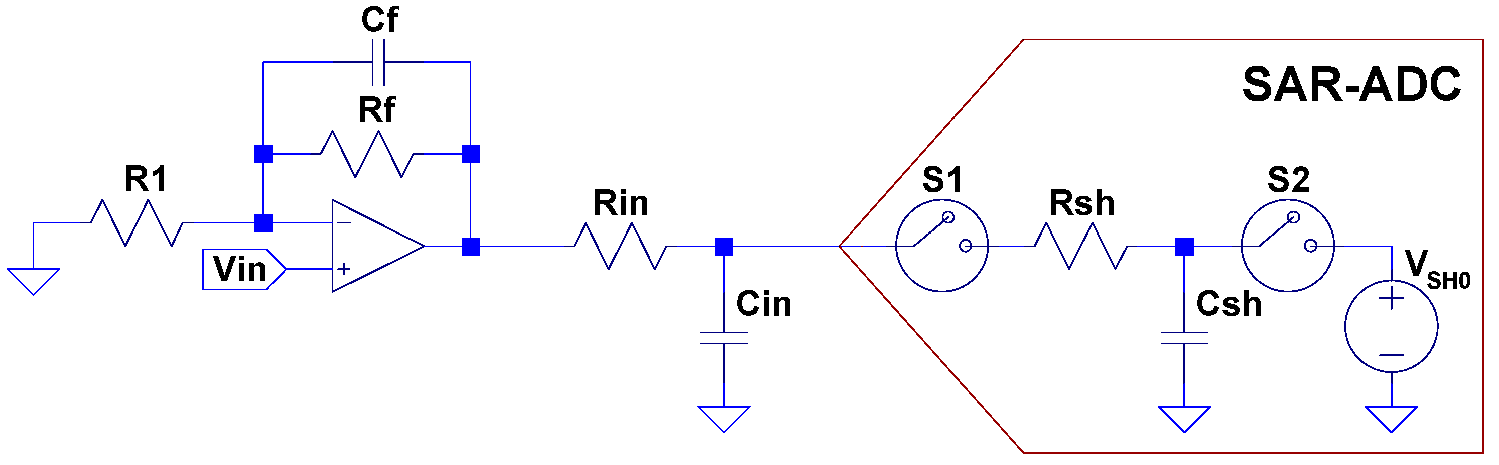
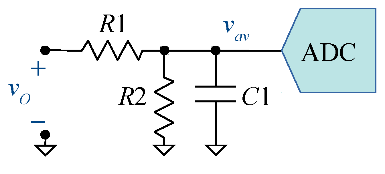
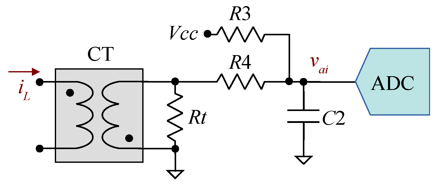
Successive approximation register (SAR) analog-to-digital converter (ADC) manufacturers recommend the use of a front-end circuit that consists of two parts: a driving amplifier and an RC filter [
1,
2]. The former can be used to implement a low pass anti-aliasing filter as shown in
Figure 1; the
,
components are needed to isolate the driving circuit from the kick due to the switched capacitors of the ADC’s input structure. Selection of the amplifier and
,
values are critical to achieving the best performance [
3].
The sensor can be connected directly to the SAR-ADC without any input driver amplifier in applications where the input signal bandwidth is much smaller than the sampling frequency. However, this low-cost solution requires the input signal to settle to within 1/2 of the least significant bit (LSB) to maintaining the conversion accuracy [
4]. ADC’s acquisition time increases, and this dramatically reduces the throughput rate. Removing the input driver amplifier can have other advantages besides lowering the cost. The designer is no longer concerned with the noise or distortion introduced by the driver amplifier itself. Another potential problem avoided is the dynamic requirements that are placed on the amplifier by the ADC, and the stability issues inherent to any closed-loop structure.
Several error compensation methods for ADC are reviewed in [
5]. Track and hold non-linearity of a high-performance ADC is modeled in [
6], and a digital algorithm is proposed to reduce the distortion. Recent advances in methods to raise the performance of SAR-ADC are summarized in [
7]. Nevertheless, none of the works focus on the errors resulting from removing the driver amplifier in the acquisition chain.
This paper proposes a simple digital correction method to get over the throughput limitation due to the settling time when driving the ADC without any amplifier. The method is based on the approximation of the sample and hold (SH) circuit by a first-order RC network. The correction is performed by only one addition and multiplication per sample.
In addition to low-demanding consumer applications, this innovative solution can be utilized in medium-throughput systems. For instance, in this paper, it is applied to the power measurement of a domestic induction heating (DIH) appliance, where low-cost implementation is required [
8].
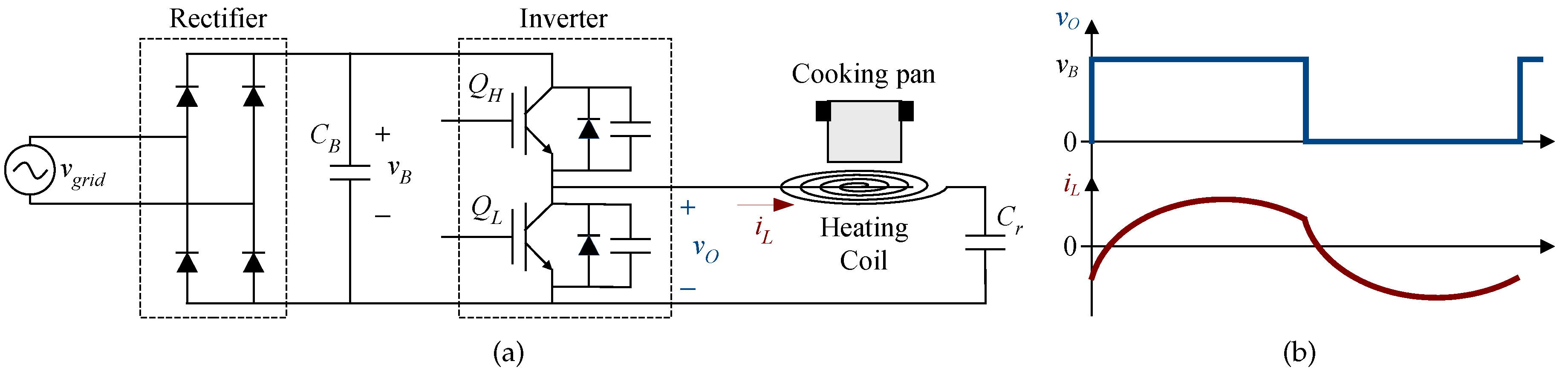
Figure 2a shows the schematic of the power converter considered. It is based on a half-bridge series resonant inverter (HBSRI). The bus voltage (
) is a full-wave rectified mains waveform filtered with a bus capacitor (
) designed to allow a big ripple. The power delivered to the load is controlled by varying the operating switching frequency (
) usually in the range of 30–75 kHz [
9].
Several methods have been reported to measure the output power for DIH. The most accurate method is to acquire the load voltage drop and the current that flows through the inductor by two ADCs with a high enough sampling rate and resolution. However, given the low-cost context of DIH applications, and assuming the equivalent series resistance (ESR) of the resonant capacitor is negligible, a similar accuracy in the computation of the power can be achieved by acquiring only the inverter output voltage (
) and the inductor current (
) (
Figure 2). Since DIH is a cost-oriented application, first-order and second-order single-bit sigma-delta ADCs have also been reported [
10,
11].
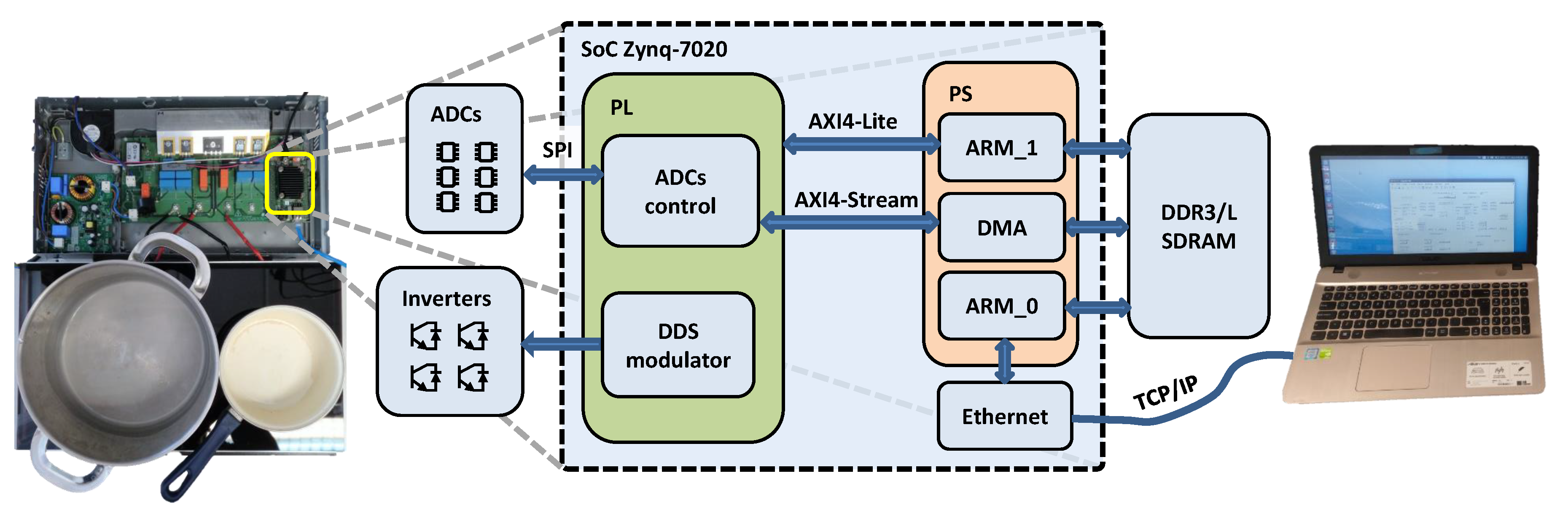
In this work, two SAR-ADCs in the range of several MSPS are used to acquire the inverter output voltage and the inductor current. The digital correction method is implemented in a system-on-chip (SoC), whose architecture integrates the processing system (PS)—based on a dual-core ARM Cortex-A9 processor—and the programmable logic (PL), which consists of field-programmable gate array (FPGA) fabric [
12]. These two parts communicate to each other through the Advanced eXtensible Interface (AXI) 4. Although an SoC is used for the validation of the proposal, given the low-cost framework of DIH applications, the final implementation of the proposed algorithms would target the application-specific integrated circuit (ASIC) or the microcontroller already available for control and protection purposes of the power converter.
This paper is organized as follows.
Section 2 develops the correction method and describes the laboratory setup utilized in this work.
Section 3 reports the experimental results. Finally,
Section 4 summarizes the main conclusions.
3. Results
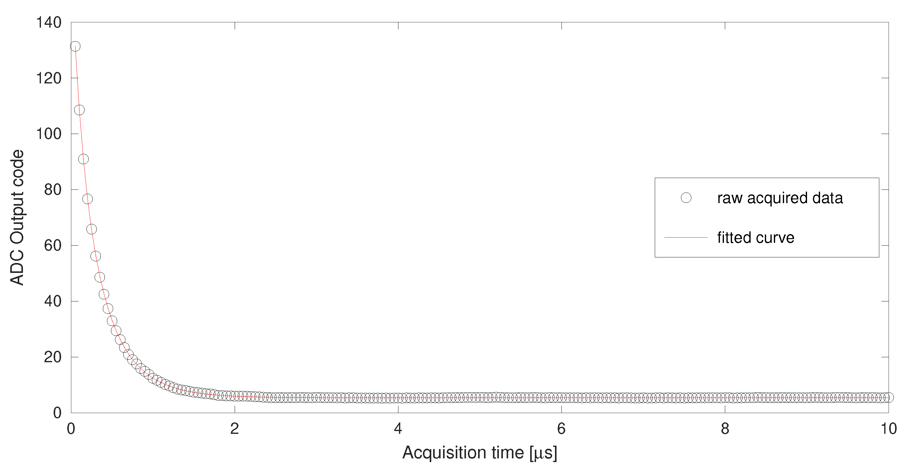
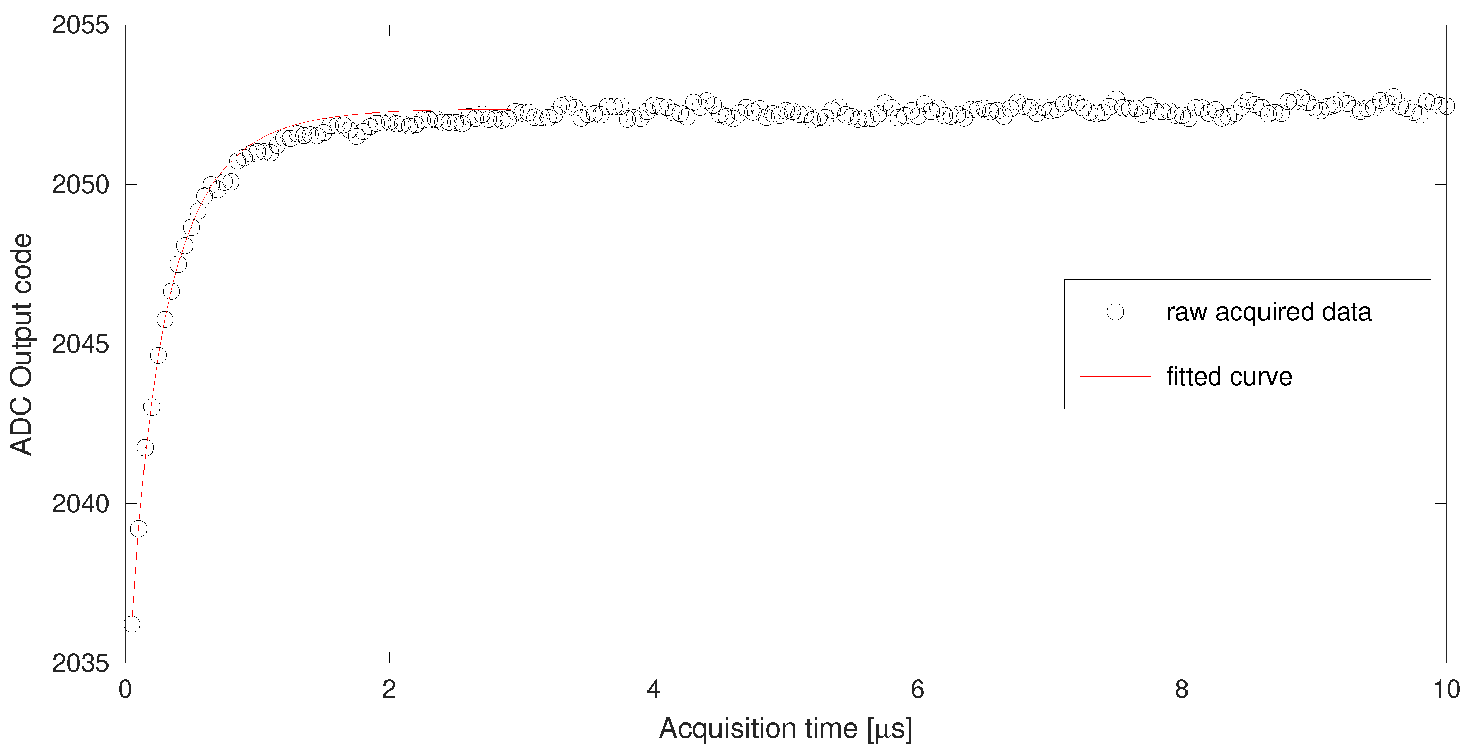
Figure 8 shows the acquired voltage fitting for zero output voltage. The acquisition time spans 10 μs to reach a deep stationary state. The average of the last microsecond data is used as
in (
18). The optimization process has been performed on the first six data with
in the range 50–300 ns with 50 ns steps. The minimization of the sum of squares of the differences (
variable in
Figure 5) results in a value of 0.3154. Such a low value explains the very good agreement of the data with the fitted curve.
Figure 9 shows the acquired current fitting for zero load current. The optimization process has also been performed on six data with
in the range 50–300 ns. The raw acquired data present an appreciable ripple due to the switched-mode voltage source that generates
in
Figure 6. However, the data are closely fitted to the curve, especially for low acquisition times.
The resulting values of the parameters found with the minimization process are summarized in
Table 3.
Three magnitudes have been selected to verify the improvement achieved by the correction method: the RMS value of the output voltage (), the RMS value of the load current (), and the average power delivered to the load (). All magnitudes have been computed over one half-cycle of the AC source.
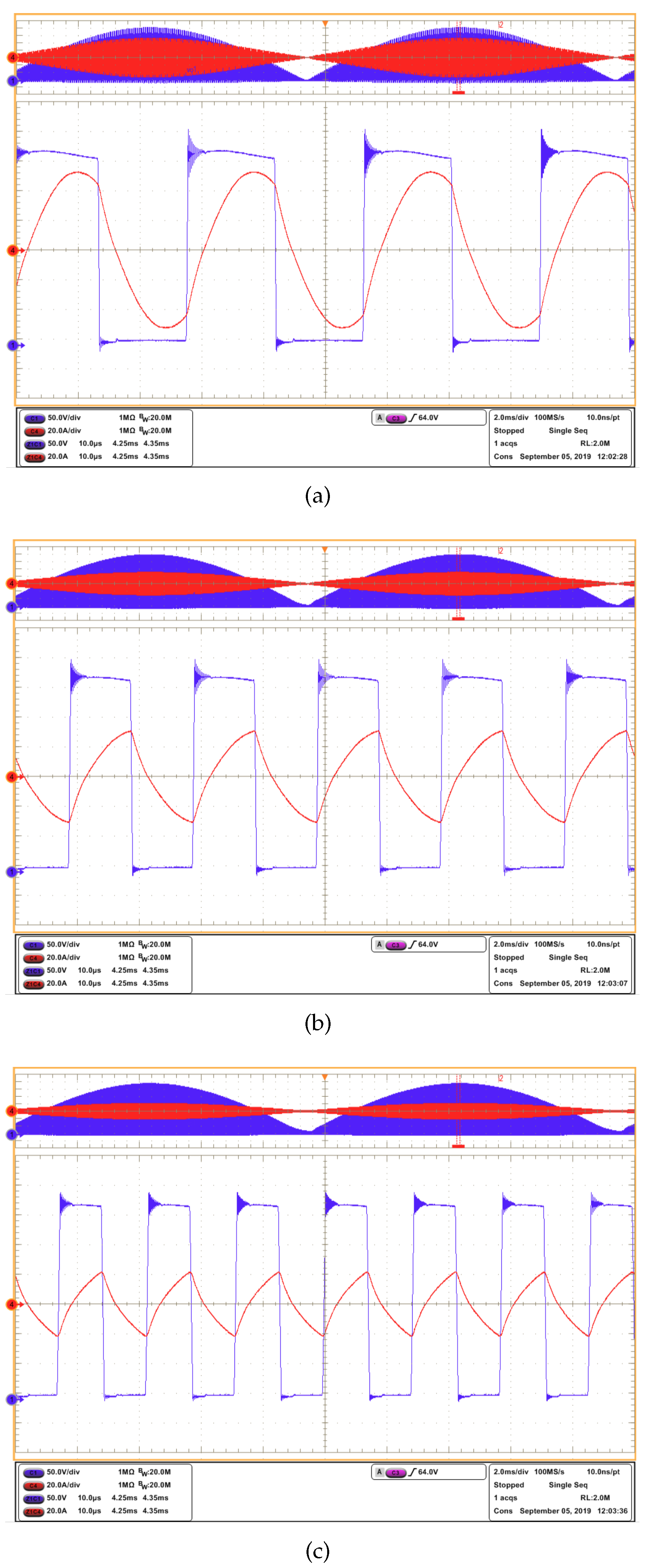
Figure 10 shows the inverter waveforms—voltage and current—captured with the oscilloscope at three switching frequencies in the range of interest.
Table 4 shows the RMS voltage, RMS current, and power computed from the oscilloscope measurements, for the three switching frequencies.
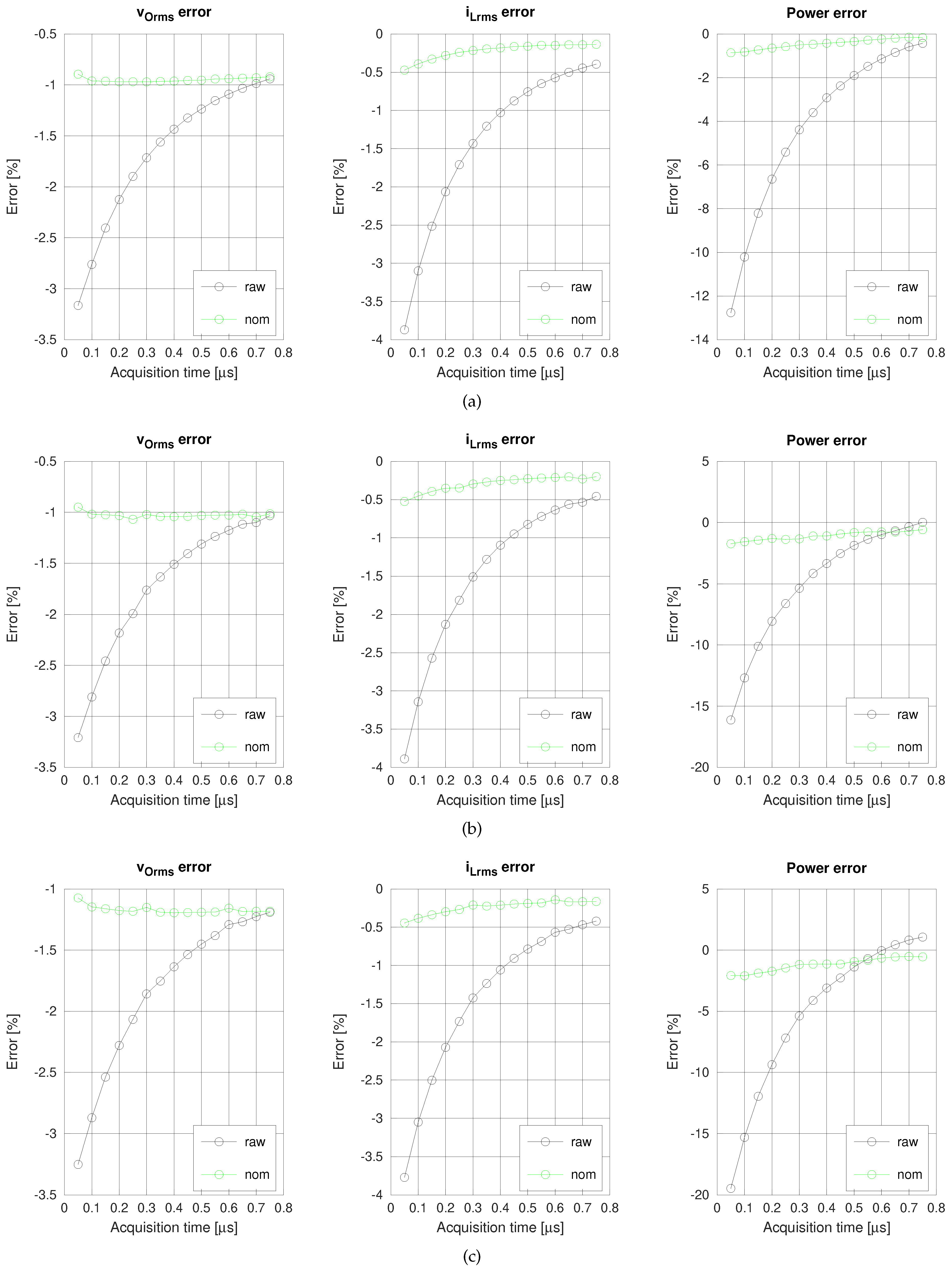
Figure 11 compares the errors obtained from the raw-acquired data (raw) with the errors once corrected with nominal values (nom), for different acquisition times. The results for three switching frequencies are shown.
Figure 11a corresponds to a low switching frequency (35 kHz), which delivers the highest power.
Figure 11b corresponds to a medium switching frequency (50 kHz), and
Figure 11c corresponds to a high switching frequency (70 kHz), which delivers the lowest power.
Without correction, voltage, current, and power errors decrease asymptotically as the acquisition time increases, provided the sampling frequency is enough to capture the harmonics of interest. If we had further increased the acquisition time, the errors would have grown due to the corresponding reduction of the sampling frequency. The maximum errors in absolute value are in the range of 3–4% for the voltage and current, and 13–20% for the power. Applying the correction method, even with nominal values, raises clearly the accuracy, with errors around 1% for the voltage and current, and less than 2% for the power.
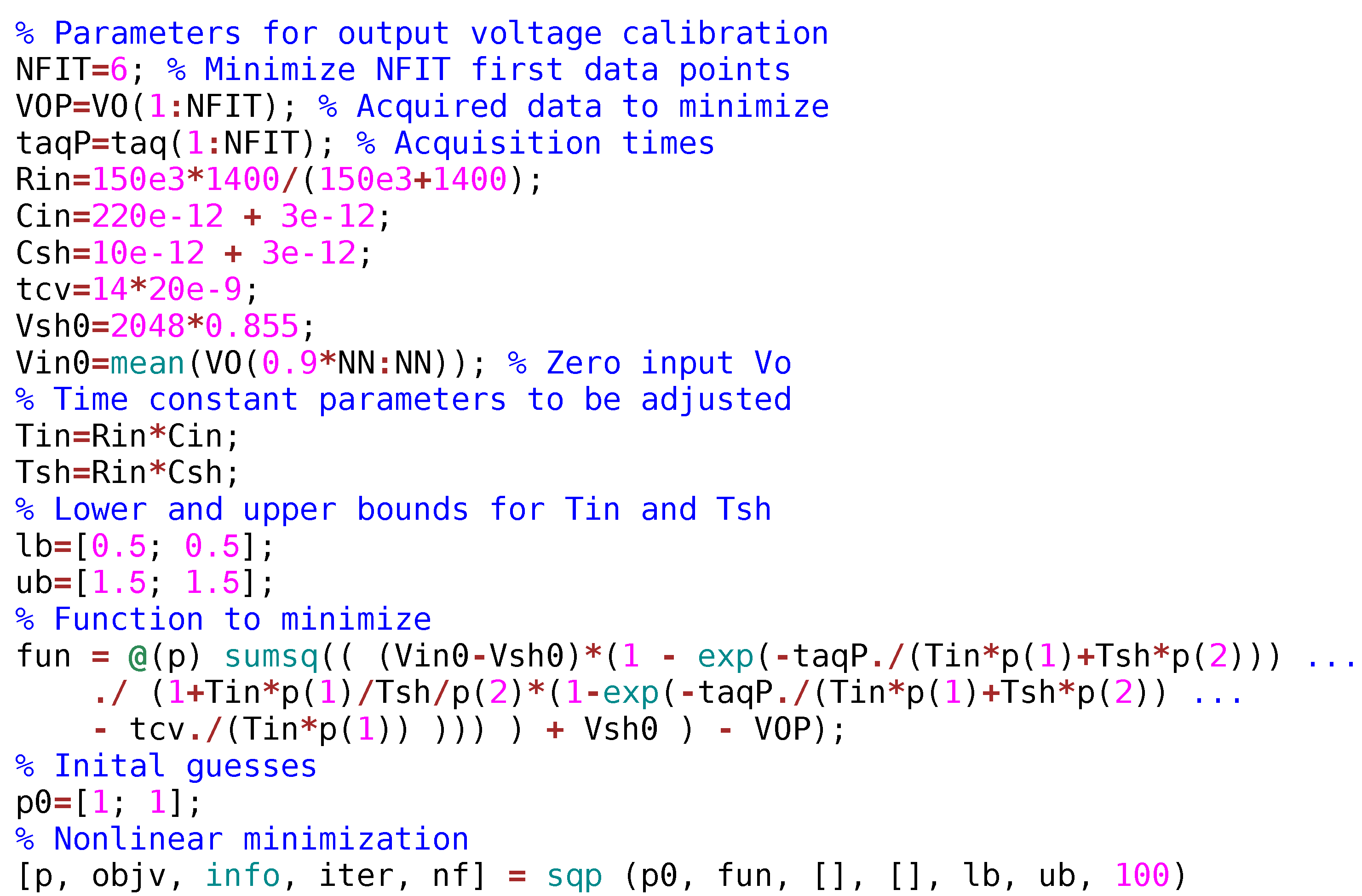
The accuracy can be further raised by using the parameters found by the minimization process.
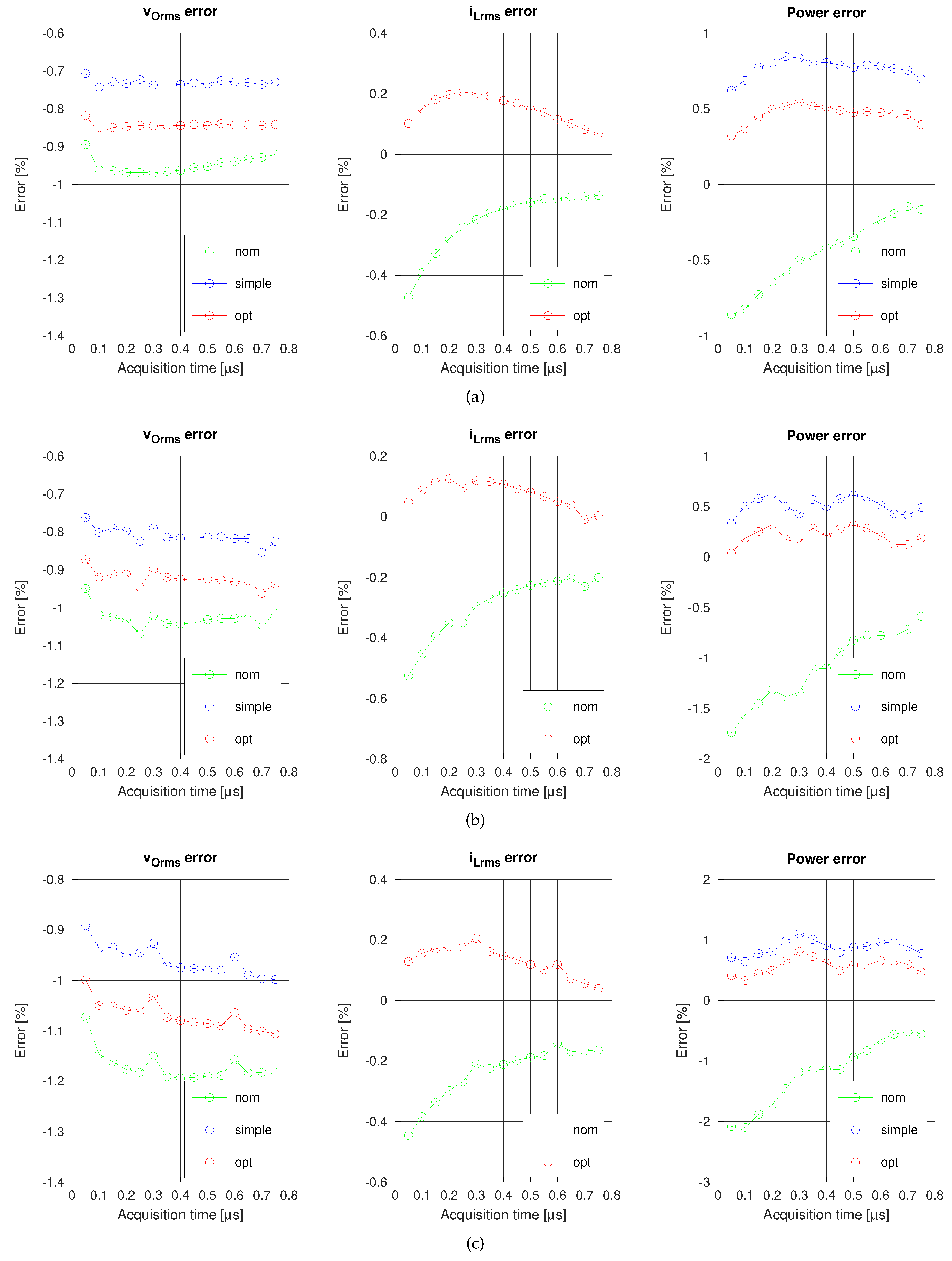
Figure 12 compares the errors when the measurements are corrected with nominal values (nom), the simple calibration process for voltage (simple), and the optimization-based method (opt). Results for the same switching frequencies as above are shown.
In all of the calibrated cases, the errors are decreased respect of the nominal case. More relevantly, the dependence of the error on the acquisition time has been reduced. The error curves for the simple and optimized cases are more horizontal than the nominal curves, especially for the current and power. Finally, it can be noticed that the worst behavior is for
Figure 12c—the highest switching frequency case—surely due to the reduced range of the current to be measured in this case.
Table 5 summarizes the average and standard deviation of the power errors for the simple and optimized calibration methods. The fifteen acquisition time data points in the 50–750 ns range have been considered for computing the metrics. The simple calibration method achieves a worst-case average error of 0.87%, while the optimization-based method slightly reduces the worst-case average error (0.57%). The standard deviation is less dependent on the method, with a worst-case value of approximately 0.12%
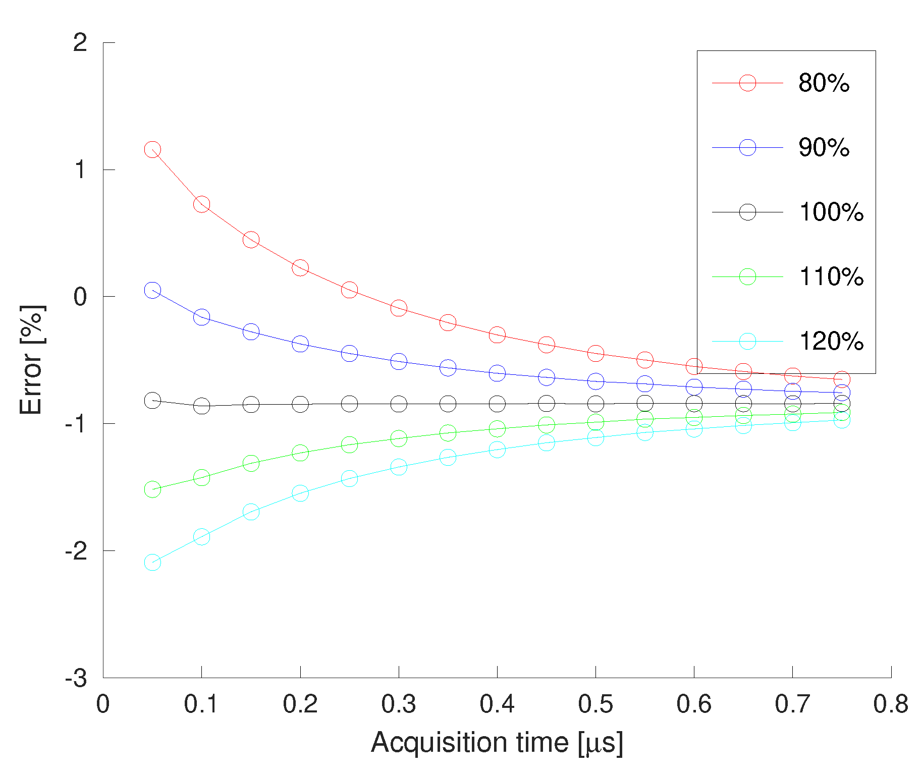
The value of
must be selected carefully to achieve such a low error. The former experimental results have been obtained with a nominal
.
Figure 13 shows the effect of changing
on the RMS output voltage error. Five values of
have been considered in the range 80–120% of its nominal value. Having a horizontal error curve with the acquisition error is a warranty of a good
selection.
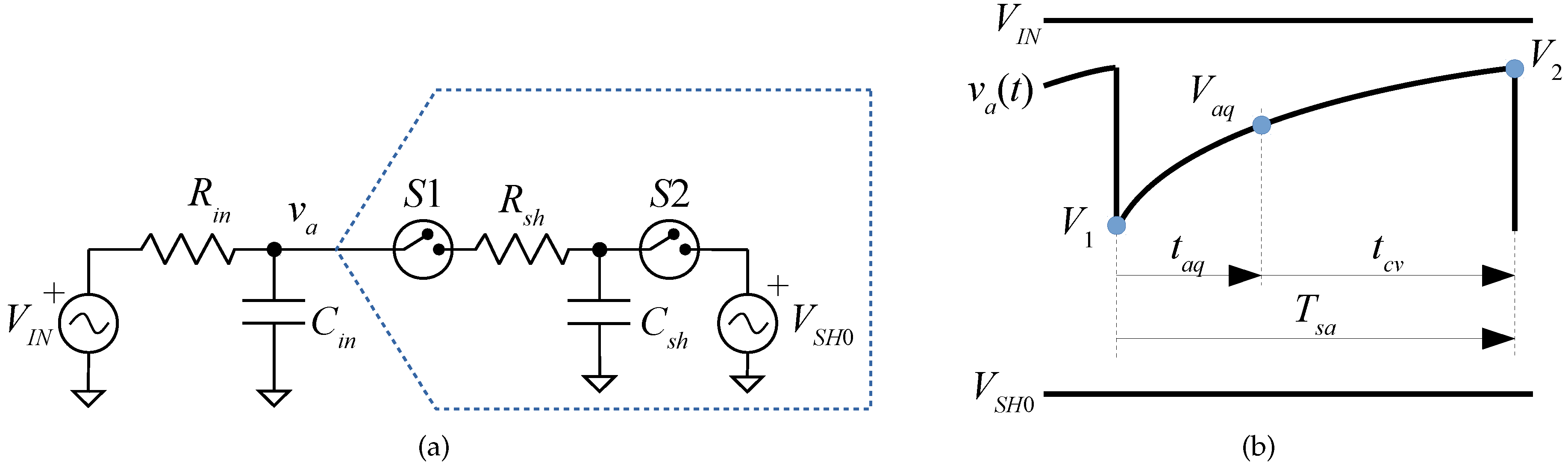
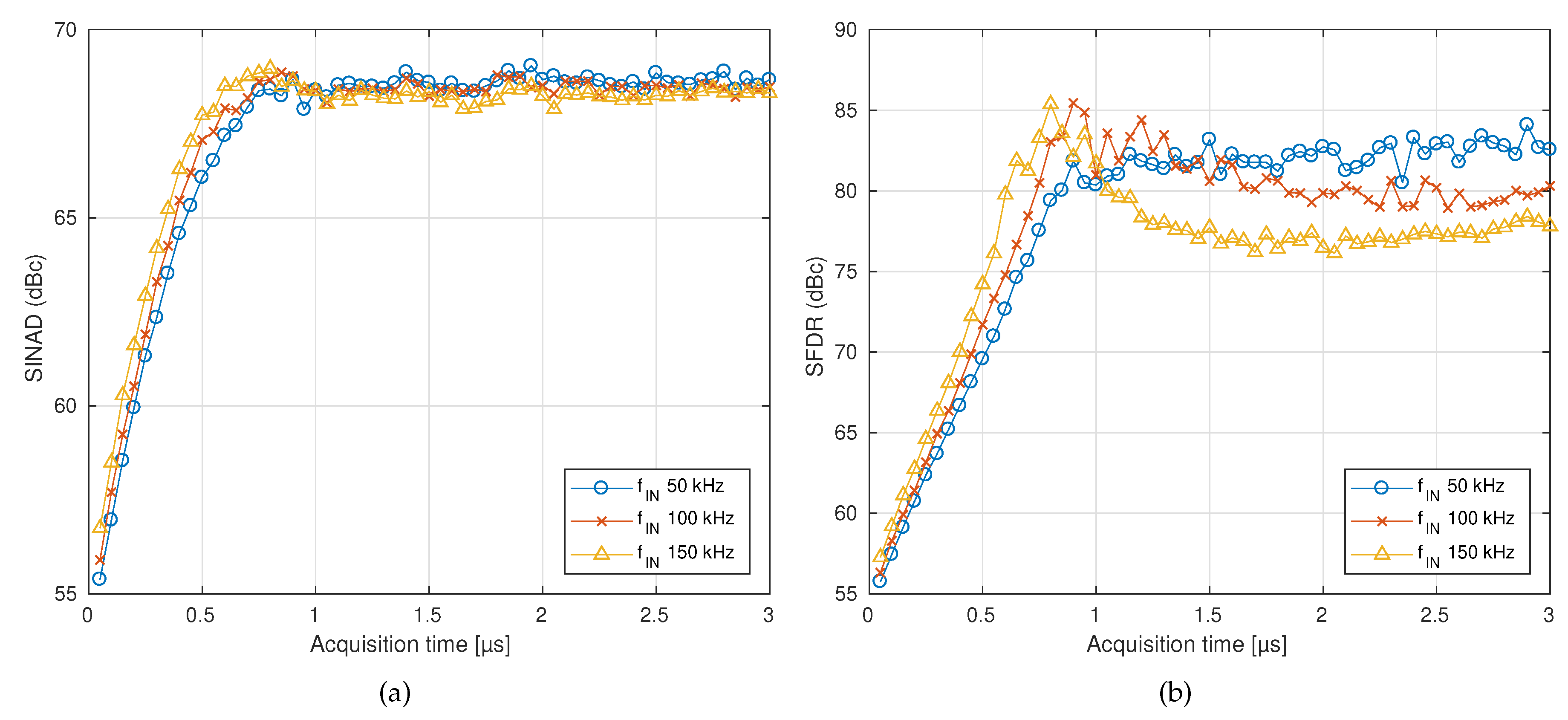
Although this work is strictly focused on averaged parameters like power or RMS values, the ADCs are used under conditions their manufacturer does not recommend. The sampling process contains non-linear terms that degrade the performance of the conversion-chain when the 1/2 LSB constraint is ignored. This degradation can not be compensated with a linear method, so it could reduce the effective number of bits (ENOB) for instantaneous measurements. Some spectral quality parameters or frequency domain performance of the ADCs, for different times, have been measured. To do so, the circuit shown in
Figure 4 was slightly modified:
and
were removed and their equivalent parallel resistance was placed between the positive terminal of
and the input of the ADC. A waveform generator was connected to the input of the circuit and sinusoidal signals with the full-scale range (FSR) of the ADC at different frequencies were captured with different
. For every case, 16k points were captured and the signal-to-noise and distortion ratio (SINAD) and spurious-free dynamic range (SFDR) were computed. The results of these two parameters are shown in
Figure 14. It can be seen how the spectral quality of the ADC is reduced when low
values are imposed. Below 0.7 μs, the ENOB is reduced, but between 0.3–0.7 μs the reduction is less than 1 bit.
4. Discussion
A method to digitally compensate the errors due to the fact of not meeting the voltage settling constraint of 1/2 LSB, on SAR-ADCs without driver amplifiers, has been analyzed and experimentally tested. It is intended to reduce the cost, size, and power consumption of the conditioning front-end by eliminating the need for a driver amplifier. The compensation can be easily performed by the digital system in charge of the ADC’s control because it involves only one addition and one multiplication per sample.
The method has been experimentally applied to the output voltage and load current of a series resonant inverter operated in the switching frequency range of 35–70 kHz. Three relevant quantities have been computed from the acquired signals: the RMS output voltage, the RMS load current, and the power delivered to the load. All magnitudes have been computed over one half-cycle of the mains AC source.
The output voltage and load current have been captured by two SAR-ADCs driven with passive conditioning circuits. The SAR-ADCs are managed by a Zynq SoC that allows changing the acquisition time in integer multiples of the clock period. The voltage and current have been captured with acquisition times in the range 50–750 ns to investigate the error dependence on the acquisition time. The reference voltage and current to compare with have been captured with an oscilloscope in high-resolution mode and high sampling frequency.
Without any correction, voltage, current, and power errors decrease as the acquisition time increases. The maximum errors in absolute value are in the range of 3–4% for the voltage and current, and 13–20% for the power. The errors increase with the switching frequency.
A correction method based on the approximation of the ADC’s sample and hold circuit by a first-order RC network has been proposed to raise the accuracy. This method requires computing two correction parameters—
and
—that depend on several circuit values ((
10) and (
11)). The parameters
and
can be computed from the nominal circuit values, obtaining the so-called nominal correction method. This method raises the accuracy, with resulting errors around 1% for the voltage and current, and less than 2% for the power.
The accuracy can be further increased by using the parameters found by a calibration process. Two possibilities have been proposed for the voltage: the simple method and the optimization-based method. Both are based on performing one first acquisition with a zero input signal. Only the optimization-based calibration method is available for the current.
Experimental results show that the errors for the calibrated cases are smaller than for the nominal case. More relevantly, the dependence of the error on the acquisition time is reduced. The error curves for the simple and optimized cases are more horizontal than the nominal curves, especially for the current and power. The simple calibration method achieves a worst-case average error of 0.87%, while the optimization-based method slightly reduces the worst-case average error (0.57%). The standard deviation is less dependent on the method, with a worst-case value of approximately 0.12%. Moreover, the calibrated methods can take into account variations due to manufacturing tolerance, temperature dependence, and aging of the components.
Therefore, depending on the accuracy constraints, we can select to apply the correction method with nominal values, or with the values found by the simple or optimization-based methods.
Table 6 summarizes the applicability and complexity of the proposed correction methods.
Further work must be done to test the proposed acquisition and correction schemes to computing more parameters from the acquired signals. This paper has focused on computing some relevant averaged parameters—RMS values and power—but the operation and control of the power converter will require some other instantaneous or temporal parameters: peak current, switches’ turn on and turn off currents, or delay between current and voltage. From the results of the SINAD and the SFDR, it can be concluded that avoiding the driver amplifier in applications where high-accuracy instantaneous measurements are obtained from high-resolution ADCs may not be recommendable for low acquisition times. Nevertheless, the proposed method offers a good accuracy in the computation of averaged parameters even for very low acquisition times.
Future work will also address the online implementation of the optimization-based calibration methods. In this paper, a non-linear optimization algorithm has been implemented on a PC running Octave for proof-of-concept purpose. As this algorithm is intended to correct slow aging or temperature variations, it might be run a few times, typically once every several minutes. The ARM Cortex-A9 available on the Zynq SoC can be programmed to run a reduced version of this algorithm.


