Abstract
This paper presents a versatile tunable voltage-mode biquadratic filter with five inputs and three outputs. The proposed filter enjoys five single-ended output operational transconductance amplifiers (OTAs) and two grounded capacitors. The filter can be easily transformed into a quadrature oscillator. The filter with grounded capacitors is resistorless and electronically tunable. Either a voltage-mode five-input single-output biquadratic filter or a voltage-mode single-input three-output biquadratic filter can be operated by appropriate selecting input and output terminals. In the operation of five-input single-output biquadratic filter, the non-inverting lowpass, non-inverting bandpass, inverting bandpass, inverting highpass, non-inverting bandreject, inverting bandreject, and non-inverting allpass filtering responses can be realized by appropriately applying the input voltage signals. In the operation of single-input three-output biquadratic filter, the non-inverting/inverting lowpass, bandpass and bandreject filtering responses can be realized simultaneously. The circuit provides independent adjustment of the resonance angular frequency and quality factor, high-input impedance, and no inverting-type input voltage signals are imposed. The application in quadrature oscillator exhibits independent electronic tuning characteristic of the oscillation condition and the oscillation frequency. The theoretical analysis has been verified through OrCAD PSpice and furthermore by experimental measurements.
1. Introduction
Active filters and oscillators are widely used in sensor, communication, instrumentation and control applications [1,2,3,4,5,6,7,8]. Especially in the sensor system, the filter is used to filter out the noise in the system [1]. Oscillators can produce a repetitive electronic signal for sensors [2,3,4,5,6]. One of the key circuits in front-ends of sensors is the quadrature signal generator for modulation and demodulation [7]. The quadrature signal generator will generate a pair of in-phase and quadrature phase signals for phase shift keying modulation in direct conversion systems. Moreover, the quadrature signals can be used to reduce the signal’s bandwidth to simply the sensor’s design [8].
Active filters with high-input impedance are of great interest because it can be easily cascaded to synthesize high-order filters [9]. Multiple-input single-output universal biquadratic filters with different filter responses are realized according to the selected different input signals, and they can realize all the five standard biquadratic filtering response filters. An attractive feature of single-input three-output multifunction biquadratic filters is that lowpass, bandpass, and highpass/bandreject outputs are simultaneously available in various circuit modes. These additional outputs can be used in systems that employ more than one filter function. The filters using operational transconductance amplifiers (OTAs) with multiple-input single-output or single-input three-output, along with capacitors, a class of OTA-C circuits are the attention for much research [10,11,12,13,14,15,16,17,18]. These designs of OTA-C filter circuits require no resistors, hence, they are suitable for integrated circuit (IC) than the other active components. Moreover, OTA-C filter circuit provides an electronic tunability of its transconductance gain, gm, and is also beneficial for compensating the process tolerances.
The recently reported electronically tunable OTA-based multiple-input single-output voltage-mode universal biquadratic filters have been proposed [19,20] that can realize all five standard filtering responses with the following four attractive advantages: (i) orthogonal controllability of the parameters resonance angular frequency (ωo) and quality factor (Q), (ii) possession high impedance at input terminal, (iii) all grounded passive components, and (iv) no need to employ inverting-type input voltage signals. The circuit [19] also permits resistorless realization along with two grounded capacitors but the parameters ωo and Q cannot be independently controllable. Although the circuit [20] permits independent of the parameters ωo and Q, it cannot achieve resistorless structure. Both the circuits in [19,20] need to use six OTAs as the active devices and cannot simultaneously realize lowpass, bandpass, and bandreject filters from the same configuration.
This study proposes a versatile voltage-mode biquadratic filter with five inputs and three outputs. The proposed circuit employs five single-ended output OTAs and two grounded capacitors. When operating in five-input single-output universal biquadratic filter, the non-inverting lowpass (LP), non-inverting bandpass (BP), inverting bandpass (IBP), inverting highpass (IHP), non-inverting bandreject (BR), inverting bandreject (IBR), and non-inverting allpass (AP) filtering responses can be obtained by the selections of different input voltage signals. When operating in single-input three-output biquadratic filter, either the LP, IBP, BR filtering responses or the inverting lowpass (ILP), BP and BR filtering responses can be simultaneously realized. Therefore, the circuit realizes single-input three-output biquadratic filter or five-input single-output biquadratic filter into single topology. The circuit also can be transformed into a quadrature oscillator. The proposed circuit enjoys the following advantages: (i) the employment of only five single-ended output OTAs, (ii) the employment of only two grounded capacitors, and thus can absorb equivalent shunt capacitive parasitics, (iii) capability to realize IBP/BP, LP/ILP and BR/IBR filtering responses simultaneously with single-input three-output, (iv) independent control of the LP, ILP, BP and IBP gains simultaneously without affecting the parameters of ωo and Q, (v) realization of all five standard filtering functions with five-input single-output by appropriate selecting different five input voltage signals, (vi) possession high-input impedance, (vii) no need to employ inverting-type input voltage signals, (viii) independent electronic adjustment of the parameters ωo and Q, (ix) easy transformed into a quadrature oscillator, and (x) low active and passive sensitivity performances. Table 1 compares the proposed filter with recently reported voltage-mode OTA-based biquadratic filters [19,20]. Unlike the reported voltage-mode OTA-based biquadratic filters in [19,20], the attractive feature of the proposed filter is that it employs only five single-ended OTAs and two grounded capacitors for realizing voltage-mode biquadratic filter and capability to realize IBP/BP, LP/ILP and BR/IBR filtering responses simultaneously with single-input three-output. Moreover, the LP, ILP, BP and IBP gains can be independently controlled simultaneously without affecting the parameters of ωo and Q. The proposed circuit also can be converted into a quadrature oscillator.

Table 1.
Comparison of recently proposed operational transconductance amplifier (OTA)-based voltage-mode filters in [19,20].
2. Circuit Descriptions and Realizations
2.1. Proposed Electronically Tunable Voltage-Mode Biquadratic Filter
The proposed electronically tunable voltage-mode biquadratic filter is shown in Figure 1. It uses only five OTAs, two grounded capacitors and no resistors which is beneficial from the IC fabrication point of view. The five input signals, Vi1, Vi2, Vi3, Vi4, and Vi5, are connected to the high-input impedance input nodes of OTAs, respectively. Therefore, the proposed circuit enjoys the advantage of having high-input impedance. An ideal OTA has infinite input and output impedances. The output current of an OTA is given by IO = gm (V + −V-) where gm is the transconductance gain of the OTA [19,20]. Routing analysis of the circuit depicted in Figure 1 yields the following OTA-C filter three output voltages.
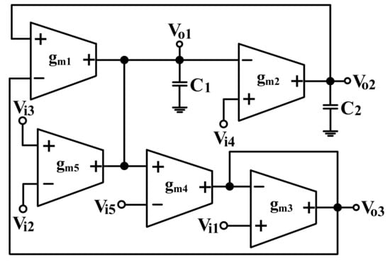
Figure 1.
Proposed electronically tunable voltage-mode biquadratic filter.
Denominator D(s) is given by
The parameters of ωo, Q and bandwidth ωo/Q given in Equation (4) are calculated as
Based on Equation (5), the parameter ωo can be tuned through gm1 and gm2, and the parameter Q can be adjusted independently through gm3 and gm4 without disturbing ωo. After adjusting ωo, the parameter Q can be adjusted independently by the ratio of gm3 and gm4, and a large Q value can be obtained by adjusting this ratio. In other words, the circuit offers orthogonal control of the parameters of ωo and Q. Note that by selecting gm1 = gm2 = gm, the parameters of ωo and Q in Equation (5) becomes
According to Equation (6), the parameter ωo can be adjusted independently by varying gm, while the parameter Q can be adjusted independently by varying gm3 and gm4. This means that the parameters of ωo and Q of the filter can be independently controlled.
2.1.1. Single-Input Three-Output Voltage-Mode Biquadratic Filter
According to Equations (1)–(3), The IBP, LP and BR signals can be simultaneously obtained by setting the input voltage Vi2 = Vi3 = Vi4 = Vi5 = 0 (grounded) and getting Vi1 as input signal Vin. The three voltage transfer functions obtained are
Thus, the circuit realizes an IBP signal at Vo1, a LP signal at Vo2, and a BR signal at Vo3, simultaneously. The IBR, LP, and BR gain constants in Equations (7)–(9) are
Similarly, The BP, ILP, and IBR signals can be simultaneously obtained by setting the input voltage Vi1 = Vi2 = Vi3 = Vi4 = 0 and getting Vi5 as input signal Vin. The three voltage transfer functions obtained are
Thus, the circuit realizes a BP signal at Vo1, an ILP signal at Vo2, and an IBR signal at Vo3, simultaneously. The BP, ILP and IBR gain constants in Equations (11)–(13) are
Moreover, two IBP signals and a LP signal can be simultaneously obtained by setting the input voltage Vi1 = Vi3 = Vi4 = Vi5 = 0 and getting Vi2 as input signal Vin. The three voltage transfer functions obtained are
Thus, the circuit realizes an IBP signal at Vo1, a LP signal at Vo2, and an IBP signal at Vo3, simultaneously. The two IBP gain constants and a LP gain constant in Equations (15)–(17) are
Based on Equation (18), two IBP gain constants and a LP gain constant can be independently controlled by changing gm5 without affecting of ωo and Q. This means that the circuit provides independent control of IBP and LP gains simultaneously without affecting the parameters of ωo and Q.
Similarly, two BP signals and an ILP signal can be simultaneously obtained by setting the input voltage Vi1 = Vi2 = Vi4 = Vi5 = 0 and getting Vi3 as input signal Vin. The three voltage transfer functions obtained are
Thus, the circuit realizes a BP signal at Vo1, an ILP signal at Vo2, and a BP signal at Vo3, simultaneously. The gain constants in Equations (19)–(21) are
Based on Equation (22), two BP gain constants and an ILP gain constant can be independently controlled by changing gm5 without effecting of ωo and Q. Therefore, according to Equations (18) and (22), the circuit provides independent control of the LP, ILP, BP and IBP gains simultaneously without affecting the parameters of ωo and Q. Table 2 summarizes the single-input three-output voltage-mode biquadratic filter of the transfer functions.
Table 2.
Single-input three-output filtering functions realized.
2.1.2. Five-Input Single-Output Voltage-Mode Biquadratic Filter
According to Equation (3), we consider five-input single-output in order to realize five standard filtering functions. Assuming that , where k is a scaling factor, the input-output relationship in Equation (3) can be expressed as
where in Equation (23), and are the realized time-constants. As indicated by Equation (23), the LP, BP, IBP, IHP, BR, IBR, and AP filtering functions are implemented by appropriately applying the input signal without inverting-type input signal requirements. Table 3 summarizes the five-input single-output voltage-mode biquadratic of the transfer functions according to Equation (23).
Table 3.
Fixed output Vo3 and various functions realized.
2.2. Modification of Proposed Filter as Quadrature Oscillator
It is interesting to note that the circuit of Figure 1 can be converted into a voltage-mode quadrature oscillator simply by connecting node Vo3 to Vi3 and letting Vi1 = Vi2 = Vi4 = Vi5 = 0. Figure 2 shows the proposed voltage-mode quadrature oscillator. The characteristic equation of the voltage-mode quadrature oscillator in Figure 2 is obtained as:
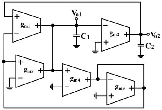
Figure 2.
Modified quadrature oscillator of Figure 1.
Inspection of Equation (24) shows that the condition of oscillation (CO) and the frequency of oscillation (FO) are given by
As indicated by Equations (25) and (26), the CO can be independently controlled by gm5 without disturbing the FO, and the FO can be independently controlled by gm2 without disturbing the CO. This means that both CO and FO are independent controllable by different transconductance gains.
Under steady state, the relationship of the two voltage outputs of Figure 2 are as
As indicated by Equation (27), the voltages Vo1 and Vo2 are in the quadrature form. Thus, the proposed circuit in Figure 1 can be easily transformed into a quadrature oscillator.
3. Effect of the OTA Parasitic Elements of the Proposed Voltage-Mode Biquadratic Circuit
The effect of OTA parasitic elements on the performance of voltage-mode filter is considered. Figure 3 depicts the simplified equivalent circuit that represents a non-ideal OTA with finite parasitic resistances and capacitances [20]. Rpj, Rnj, and Roj are the input and output terminals parasitic resistances of the jth OTA, respectively. Cpj, Cnj, and Coj are the input and output terminals parasitic capacitances of the jth OTA, respectively. In practical OTA’s the input and output parasitic conductance are very smaller the transconductance gm. In the presence of these parasitic elements, the circuit presented in Figure 1 is modified to become the circuit presented in Figure 4, in which C1p = Co1//Cn2//Cn4//Co5, C2p = Cp1//Co2, C3p = Cn1//Cn3//Co4, R1p = Ro1//Rn2//Rn4//Ro5, R2p = Rp1//Ro2, and R3p = Rn1//Rn3//Ro4. It is further noted that the proposed circuit employs external capacitors C1 and C2 parallel connecting at the output nodes Vo1 and Vo2, respectively. As a result, the effects of the parasitic capacitances C1p and C2p can be absorbed, because C1 >> C1p, and C2 >> C2p. The parasitic capacitance C1p can be absorbed in the external capacitance C1, but the presence of parasitic resistance at Vo1 output terminal would change the type of the impedance, which should be of a purely capacitive character. The parasitic capacitance C2p can be absorbed in the external capacitance C2, but the presence of parasitic resistance at Vo2 output terminal also would change the type of the impedance. To reduces its effect, one possible solution is to make the operating frequency . The parasitic impedance at Vo3 output terminal is connected a grounded impedance (R3p//C3p). This fact affects the operating frequency in the high frequency region, because C3p = (Cn1 + Cn3 + Co4). To alleviate the effects of parasitic impedance at Vo3 output terminal, the frequency of operation must be smaller than . To minimize the effects of the OTAs’ non-idealities, the useful oscillation frequency range of the proposed filter is limited by the following conditions:
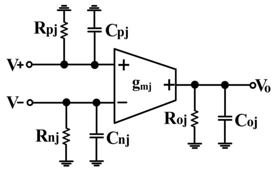
Figure 3.
Non-ideal equivalent circuit model of OTA.
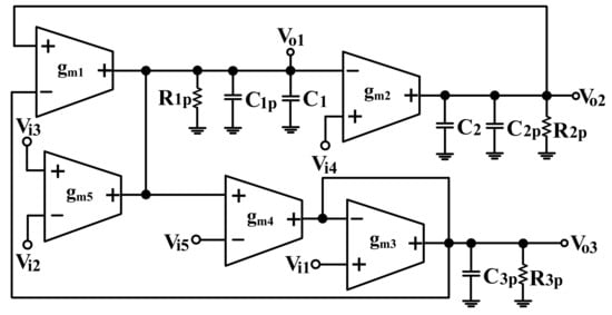
Figure 4.
Proposed voltage-mode filter including the parasitic elements of OTA.
It is not difficult to satisfy these conditions, the external capacitances C1 and C2 can be set much greater than the input and output parasitic capacitances. If the conditions of , and are satisfied, the influence of OTA parasitic elements on the proposed filter in Figure 1 can be ignored.
The active and passive sensitivities of the proposed circuits are low and not larger then unity in absolute value.
4. Simulation and Experimental Results
According to LT1228 datasheet [21], the LT1228 consists of two amplifiers to form a current feedback amplifier, which can operate from any supply voltage of ±2 V to ±15 V. The LT1228 implements gain control with a transconductance amplifier and its gain is proportional to an external controlled current. The LT1228 current feedback amplifier is an excellent buffer for transconductance amplifiers due to its very high input impedance. In addition, the LT1228 maintains a wide bandwidth over the wide voltage gain range of the current feedback amplifier that makes the transconductance amplifier output easy to connect to other circuits. The LT1228 is designed to drive low impedance loads like other current feedback amplifiers. The input signal should be less than 100 mVp to match the dynamic range of the transconductance amplifier. The LT1228 consists of transconductance amplifier and current feedback amplifier, where the transconductance amplifier converts the current into a voltage, and then the current feedback amplifier amplifies the voltage. Two specific sensor applications have been proposed in [22,23]. The proposed filter is built by LT1228, so the proposed filter can operate between ±2 V and ±15 V. The low voltage filter such as ±2 V filter can be applied to biomedical sensor systems and internet of things, and the high voltage filter such as ±15 V filter can be applied to automotive electronic sensing devices and industrial electronic sensing devices.
The performance of the proposed OTA-based voltage-mode filter and oscillator has been evaluated using OrCAD PSpice simulations based on macro-model of LT1228 OTA commercially available IC. According to LT1228 datasheet [21], the transconductance gain, gm, is given by the formula:
where ISET is the bias current of LT1228. This feature makes it useful for electronic control of transconductance gain. From the internal structure of LT1228 OTA, the current can be written as
where VBE in bipolar junction transistor is about 0.65 V and Rtun is an external resistor used for adjusting the current ISET, while VDD and VSS are the positive and negative bias voltages, respectively. Thus, the value of the resistor Rtun will be utilized to implement the desired values of the transconductance gain and make the transconductance gain electronically tunable.
4.1. Proposed Voltage-Mode Biquadratic Filter Simulation Results
OrCAD PSpice simulations based on macro-model LT1228 ICs were performed to verify the workability of the OTA-based circuit. The supply voltages were VDD = −VSS = 15 V, and the bias currents 100 µA (i.e., gm = 10 ISET [21,24]) for OTA1 to OTA5. All transconductances and capacitances were given as 1 mS and 1 nF, respectively, and were designed to obtain a OTA-based circuit in Figure 1 with an angular frequency of fo = 159.16 kHz, and a quality factor of Q = 1. Figure 5 shows the simulated gain and phase responses for the IBP (Vo1), LP (Vo2), and BR (Vo3) filters in Figure 1 with Vi1 = Vin, and Vi2 = Vi3 = Vi4 = Vi5 = 0. Figure 6 shows the simulated gain and phase responses for the BP (Vo1), ILP (Vo2), and IBR (Vo3) filters in Figure 1 with Vi5 = Vin, and Vi2 = Vi3 = Vi4 = Vi5 = 0. Figure 7 shows the five-input single-output voltage-mode biquadratic filter simulated gain responses at the Vo3 output terminal of Figure 1 by appropriate selecting different five input voltage signals. The values of C1 = C2 = 1 nF, gm3 = gm4 = gm5 = 1 mS (ISET = 100 uA), Q = 1 were maintained, and simultaneously, only gm1 and gm2 values were varied with different values of 1 mS, 1.5 mS (ISET = 150 uA), 2 mS (ISET = 200 uA), and 3 mS (ISET = 300 uA); this resulted in BP responses at the Vo1 output terminal with simulated angular frequencies fo = 156.68 kHz, fo = 235.03 kHz, fo = 313.72 kHz, and fo = 472.03 kHz, with errors of −1.56%, −1.55%, −1.44%, and −1.14%, respectively. The resulting BP filter responses with Vi5 = Vin, and Vi1 = Vi2 = Vi3 = Vi4 = 0 at the Vo1 output terminal are shown in Figure 8a, which exhibited tuning of fo without affecting Q. Next, the parameter Q was tuned without disturbing fo by keeping the values gm1 = gm2 = gm4 = gm5 and varying gm3. Figure 8b shows the tunability of Q in the BP responses with Vi5 = Vin, and Vi1 = Vi2 = Vi3 = Vi4 = 0 at the Vo1 output terminal by varying only transconductance gm3 value. As an example, values were selected to realise a constant angular frequency of fo = 159.16 kHz, the component values C1 = C2 = 1 nF, gm1 = gm2 = gm4 = gm5 = 1 mS and only varying the value gm3 = 1 mS, gm3 = 1.5 mS, gm3 = 2 mS and gm3 = 3 mS, resulting in Q = 1, 1.5, 2 and 3, respectively. These results demonstrated that tuning of the Q-value without affecting the fo-value could be performed using various value of gm3. To test the input dynamic range of the filter, the simulation was repeated for a sinusoidal input signal at fo = 159.16 kHz. Figure 9a shows that the input dynamic range of the IBP response with Vi1 = Vin, and Vi2 = Vi3 = Vi4 = Vi5 = 0 at the Vo1 output terminal with all transconductance values as 1 mS, and C1 = C2 = 1nF, which extended to an amplitude of 0.1 V (peak) without signification distortion. In Figure 9a, the percentage of the total harmonic distortion (THD) is 2.01%. The dependence of the output harmonic distortion of IBP response on input voltage amplitude is illustrated in Figure 9b. Furthermore, the intermodulation distortion (IMD) for IBP response with Vi1 = Vin, and Vi2 = Vi3 = Vi4 = Vi5 = 0 of filter output voltage Vo1 in Figure 1 is investigated. Two closely spaced tones, f1 = 158 kHz and f2 = 160 kHz, were used with equal input signal amplitudes. Figure 10 shows the dependence of the third-order IMD of IBP filter output voltage Vo1 with two input tones.
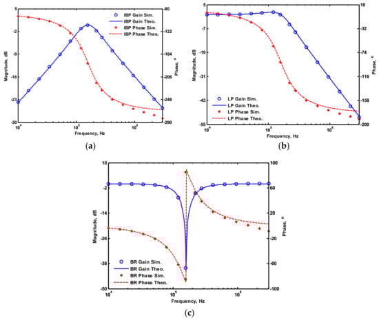
Figure 5.
Simulated gain and phase responses of Figure 1 with Vi1 = Vin, and Vi2 = Vi3 = Vi4 = Vi5 = 0 (a) inverting bandpass (IBP) filter at Vo1 terminal, (b) LP filter at Vo2 terminal, (c) BR filter at Vo3 terminal.
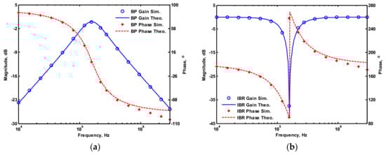
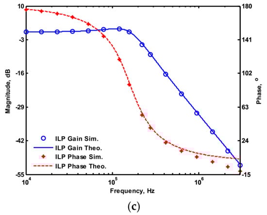
Figure 6.
Simulated gain and phase responses of Figure 1 with Vi5 = Vin, and Vi1 = Vi2 = Vi3 = Vi4 = 0 (a) BP filter at Vo1 terminal, (b) inverting lowpass (ILP) filter at Vo2 terminal, (c) inverting bandreject (IBR) filter at Vo3 terminal.
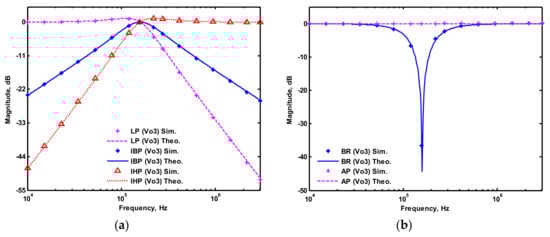
Figure 7.
Simulated gain responses of five-input single-output biquad filter at Vo3 output terminal of Figure 1 (a) LP, IBP, and IHP filters, (b) BR and AP filters.
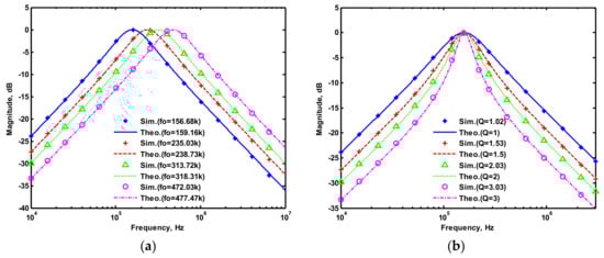
Figure 8.
Gain response of the BP (Vo1) filters, (a) varying fo while keeping Q, (b) varying Q while keeping fo.
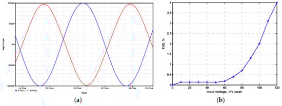
Figure 9.
Time-domain results of the IBP (Vo1) response (a) input (blue line) and output (red line) waveforms, (b) total harmonic distortion (THD) analysis results.
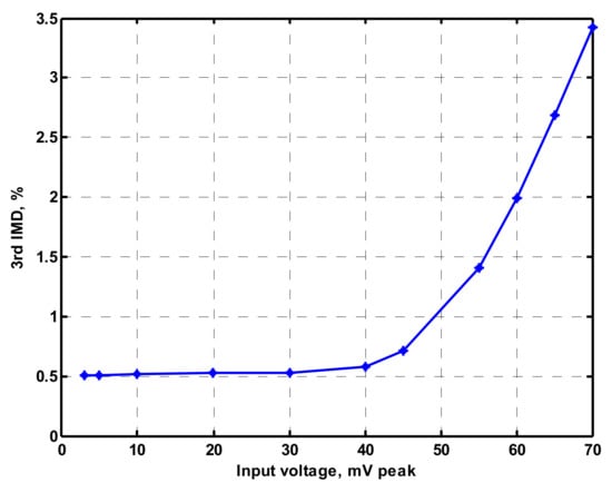
Figure 10.
Dependence of the third-order IMD of the IBP filter on input voltage amplitudes.
4.2. The Monte-Carlo Simulations
To collect statistical data regarding mismatch and the variation effect, Monte-Carlo simulations were conducted. The device mismatch was modelled as a set of randomly generated samples that represented the probability distributions of the device parameters. The proposed filter was investigated using Mont-Carlo analysis. Monte-Carlo analysis results for 100 simulations, regarding the IBP frequency responses with Vi1 = Vin, and Vi2 = Vi3 = Vi4 = Vi5 = 0 at the Vo1 output terminal with all transconductance values given as 1 mS, and C1 = C2 = 1nF, in which two capacitances C1 and C2 had a variation of 5% Gaussian deviation. Figure 11 shows the histogram of the angular frequency obtained from the Monte-Carlo analysis.
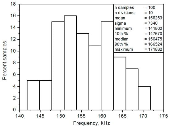
Figure 11.
Histogram of Monte-Carlo analysis for IBP filter output voltage Vo1 terminal.
4.3. Modification of Proposed Filter as Quadrature Oscillator Simulations
In order to confirm the theoretical study, the proposed voltage-mode quadrature oscillator realized in Figure 2 was also simulated using OrCAD PSpice simulation program, and the macro-model LT1228 ICs in Figure 2 was used. The supply voltages were VDD = −VSS = 15 V, and the bias currents 100 µA for OTA1 to OTA5. The quadrature oscillator was designed with gm1 = gm2 = gm3 = gm4 = gm5 = 1 mS, and C1 = C2 = 5 nF for the oscillation frequency of fo = 31.83 kHz, in which gm5 is larger than the theoretical value to ensure that oscillator will work. The simulation result of quadrature outputs, Vo1 and Vo2, is shown in Figure 12a. Figure 12b shows the lissajous pattern of Vo1 and Vo2 outputs of the simulation results.
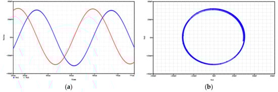
Figure 12.
Simulated quadrature voltage outputs in Figure 2 (a) Vo1 (blue) and Vo2 (red), (b) X-Y plot.
4.4. Proposed Voltage-Mode Biquadratic Filter Experimental Results
The proposed filter in Figure 1 was experimental tested. The LT1228s commercially available OTAs were used in Figure 1 with the bias currents 100 µA for OTA1 to OTA5. The component values used in Figure 1 were gm1 = gm2 = gm3 = gm4 = gm5 = 1 mS, C1 = C2 = 1 nF, and were designed to obtain a voltage-mode filter with an angular frequency of fo = 159.16 kHz. The subsequent experimental measurements were carried out using keysight E5061B-3L5 network analyzer. Figure 13 shows the measurement gain responses for the IBP (Vo1), non-inverting LP (Vo2), and non-inverting BR (Vo3) filters in Figure 1 with Vi1 = Vin, and Vi2 = Vi3 = Vi4 = Vi5 = 0. Figure 14 shows the measurement LP, IBP, IHP and BR gain responses at the Vo3 output terminal of Figure 1 by appropriate selecting different five input voltage signals. Figure 15 shows the measurement gain and phase responses for the AP (Vo3) filter in Figure 1 with Vi1 = Vi2 =Vin, and Vi3 = Vi4 = Vi5 = 0. The measured of electronic tuning the fo-value of the BP responses with Vi5 = Vin, and Vi1 = Vi2 = Vi3 = Vi4 = 0 at the Vo1 output terminal is demonstrated in Figure 16. In Figure 16, the values of C1 = C2 = 1 nF, gm3 = gm4 = gm5 = 1 mS, Q = 1 were maintained, and simultaneously, only gm1 and gm2 values were varied with different values of 1 mS, 1.5 mS, 2 mS, and 3 mS; this resulted in BP responses at the Vo1 output terminal with measured angular frequencies fo = 161.05 kHz, fo = 244.26 kHz, fo = 330.16 kHz, and fo = 505.34 kHz, with errors of 1.19%, 2.32%, 3.72%, and 5.84%, respectively. Figure 17 shows the measured of the Q-tuning without affecting the fo-value. In Figure 17, the component values C1 = C2 = 1 nF, gm1 = gm2 = gm4 = gm5 = 1 mS and only varying the value gm3 = 1 mS, gm3 = 1.5 mS, gm3 = 2 mS and gm3 = 3 mS, resulting in Q = 1, 1.5, 2 and 3, respectively.
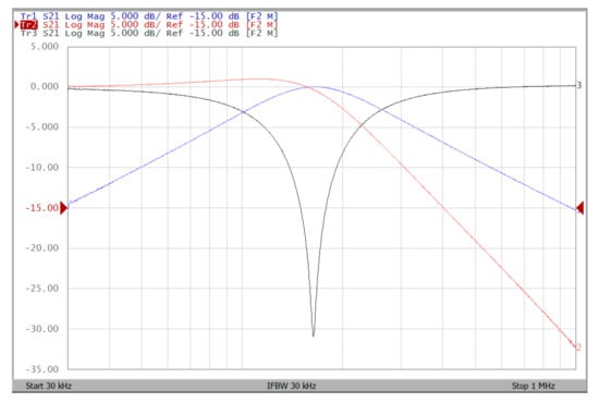
Figure 13.
Experimental results of gain responses for IBP (blue), LP (red), and BR (black) filters with Vi1 = Vin, and Vi2 = Vi3 = Vi4 = Vi5 = 0 when ± 15V DC supply.
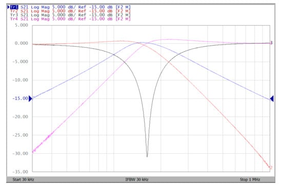
Figure 14.
Experimental results of five-input single-output biqaudratic filter at Vo3 output terminal of Figure 1 by appropriate applied input voltage signals when ±15 V DC supply.
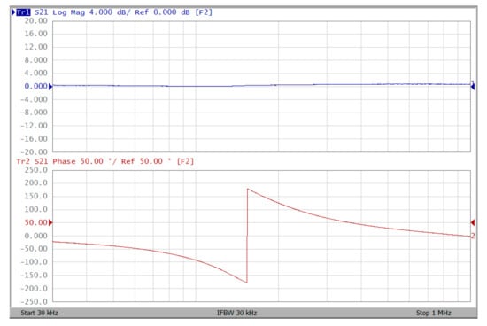
Figure 15.
Experimental results of gain (blue) and phase (red) responses for AP filter at Vo3 with Vi1 = Vi2 = Vin, and Vi3 = Vi4 = Vi5 = 0 when ± 15 V DC supply.
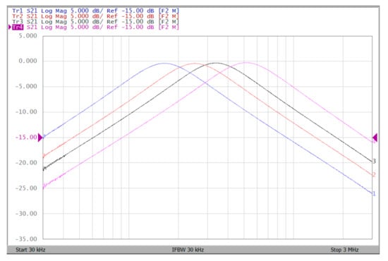
Figure 16.
Experimental results of the fo-tuning without affecting the Q-value when ±15 V DC supply.
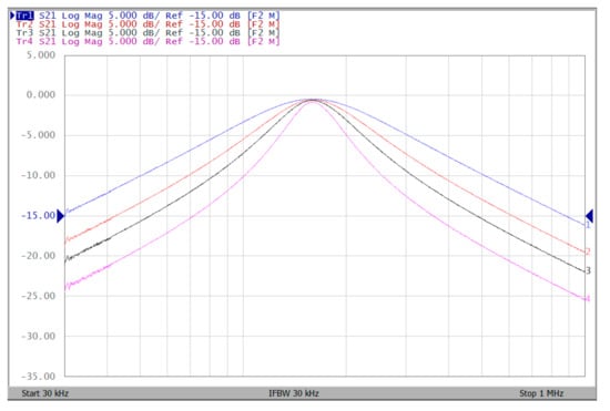
Figure 17.
Experimental results of the Q-tuning without affecting the fo-value when ±15 V DC supply.
To represent the linearity of proposed filter, the 1-dB power gain compression point (P1dB) is measured through the Agilent N9000A CXA signal analyzer. Figure 18 shows the measured of P1dB of the IBP filter output voltage Vo1 with Vi1 = Vin, and Vi2 = Vi3 = Vi4 = Vi5 = 0 by applying the input power at the angular frequency of 159 kHz. As shown in Figure 18, the measured P1dB of IBP filter is about −9.2 dBm with respect to output power. Figure 19 and Figure 20 show the spectrum of the IBP filter output voltage Vo1 through inter-modulation characterization by applying two-tone signals near 159 kHz. In Figure 19, two closely spaced tones, f1 = 158 kHz and f2 = 160 kHz, were used with equal input amplitudes of 30 mVp. The result shows that the third-order IMD is around −42.35 dBc and the third-order intercept (TOI) is around −5.66 dBm. Figure 20 shows the measured of third-order IMD is around −23.16 dBc and the TOI is around −8.531 dBm with equal input amplitudes of 70 mVp. In Figure 13, Figure 14, Figure 15, Figure 16, Figure 17, Figure 18, Figure 19 and Figure 20, the directly current (DC) power supply is ±15 V
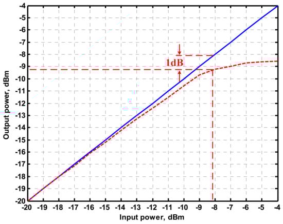
Figure 18.
Measured of P1dB of the IBP filter with input power at the Vo1 when Vi1 = Vin, and Vi2 = Vi3 = Vi4 = Vi5 = 0 when ± 15V DC supply.
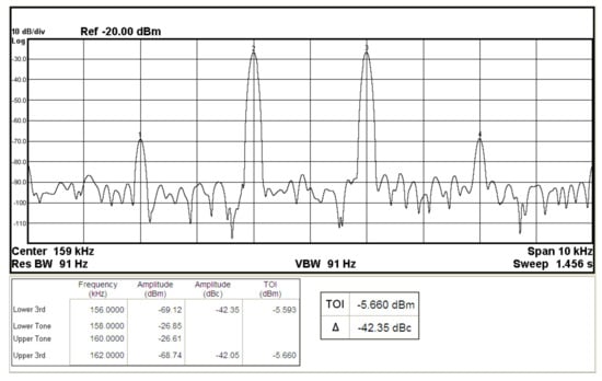
Figure 19.
The IBP filter output spectrum for a two-tone intermodulation distortion test with equal input amplitudes of 30 mVp when ±15 V DC supply.
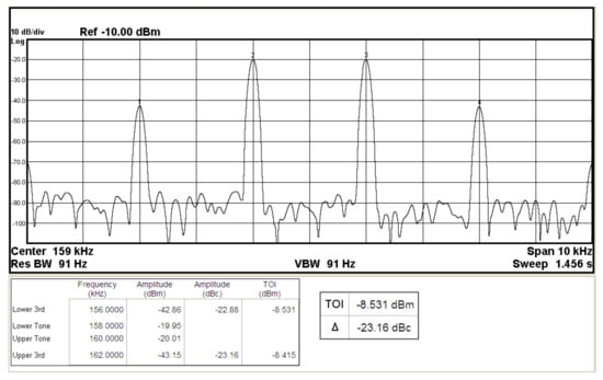
Figure 20.
The IBP filter output spectrum for a two-tone intermodulation distortion test with equal input amplitudes of 70 mVp when ±15 V DC supply.
To demonstrate that the proposed circuit can operate on a ±2 V DC supply, Figure 21, Figure 22 and Figure 23 show the results of the operation of the ±2 V DC supply in Figure 13, Figure 14 and Figure 15, which show that the proposed circuit can operate on a ±2 V DC supply. Figure 24 shows the measured of P1dB of the IBP filter output voltage Vo1 with ±2 V DC power supply by applying the input power at the angular frequency of 159 kHz. As shown in Figure 24, the measured P1dB of IBP filter is about −14.6 dBm with respect to output power. Figure 25 shows the measured of third-order IMD is around −42.86 dBc and the TOI is around −5.474 dBm with equal input amplitudes of 30 mVp when ±2 V DC supply.
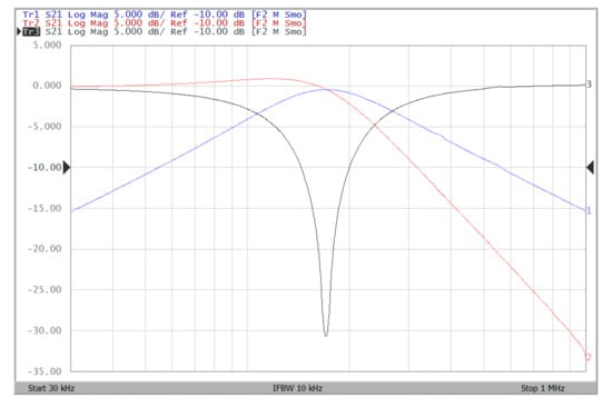
Figure 21.
Experimental results of gain responses for IBP (blue), LP (red), and BR (black) filters when ±2 V DC supply.
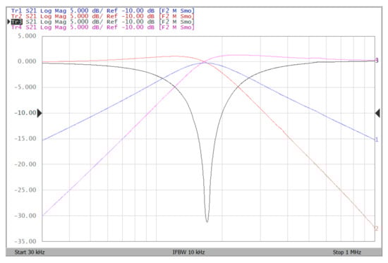
Figure 22.
Experimental results of five-input single-output biqaudratic filter at Vo3 output terminal of Figure 1 by appropriate applied input voltage signals when ±2 V DC supply.
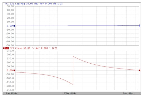
Figure 23.
Experimental results of gain (blue) and phase (red) responses for AP filter at Vo3 when ±2 V DC supply.
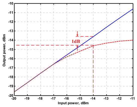
Figure 24.
Measured of P1dB of the IBP filter with input power at the Vo1 when ±2 V DC supply.
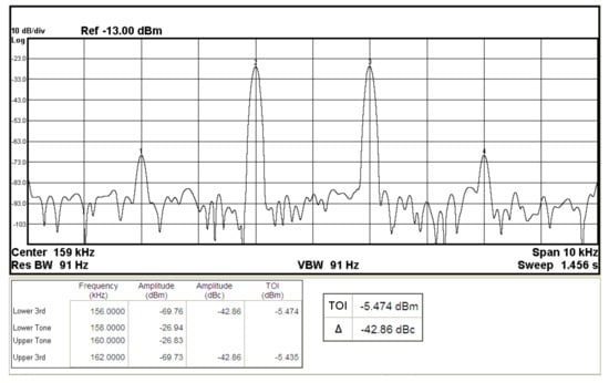
Figure 25.
The IBP filter output spectrum for a two-tone intermodulation distortion test with equal input amplitudes of 30 mVp when ±2 V DC supply.
5. Conclusions
In this paper, a new versatile tunable voltage-mode biquadratic filter with resistorless structure is proposed. The proposed circuit can be used either a single-input three-output biquadratic filter or a five-input single-output biquadratic filter with the same topology, which is more versatile than the filter one with a single input and multiple outputs or the filter one with multiple inputs and single output. The advantages of the proposed circuit are that: (i) the circuit uses only five single-ended output OTAs, two grounded capacitors and no resistors, which is attractive for its IC implementation; (ii) the circuit realizes five generic filter signals without any inverting-type voltage inputs; (iii) the circuit has high-input impedance good for cascadeability the voltage-mode circuits; (iv) the functionality of LP, BP, IBP, IHP, BR, IBR, and AP filtering functions can be easily obtained by appropriate selecting different voltage inputs; (v) the IBP/BP, LP/ILP and BR/IBR filtering responses are simultaneously available without component matching condition; (vi) independent control of the LP, ILP, BP and IBP gains simultaneously without affecting the parameters of ωo and Q, (vii) the parameters ωo and Q can be independently tunable controlled; (viii) the filter topology provides flexible modification of quadrature oscillator; (ix) low active and passive sensitivity performances. OrCAD PSpice simulations and experimental measurements using commercially available LT1228 ICs confirm the feasibility of the proposed filter.
Author Contributions
S.-F.W. and H.-P.C. conceived and designed the theoretical verifications; the optimization ideas were provided by Y.K.; H.-P.C. analysed the results and wrote the paper; Y.-C.L. performed the simulations and experiments.
Funding
This research was funded by the Ming Chi University of Technology.
Acknowledgments
We are grateful to the editors and referees for their invaluable suggestions for improving the paper.
Conflicts of Interest
The authors declare no conflict of interest.
References
- Zhao, Z.; Tong, H.; Deng, Y.; Xu, W.; Zhang, Y.; Ye, H. Single-Lead Fetal ECG Extraction Based on a Parallel Marginalized Particle Filter. Sensors 2017, 17, 1456. [Google Scholar] [CrossRef]
- Tang, Z.L.; Li, S.M.; Yu, L.J. RF spectrum sensing based on an overdamped nonlinear oscillator ring for cognitive radios. Sensors 2016, 16, 844. [Google Scholar] [CrossRef]
- Yang, M.Z.; Dai, C.L.; Shih, P.J. An acetone microsensor with a ring oscillator circuit fabricated using the commercial 0.18 um CMOS process. Sensors 2014, 14, 12735–12747. [Google Scholar] [CrossRef]
- Yang, M.Z.; Dai, C.L.; Wu, C.C. Sol-gel zinc oxide humidity sensors integrated with a ring oscillator circuit on-a-chip. Sensors 2014, 14, 20360–20371. [Google Scholar] [CrossRef]
- Chen, C.C.; Lin, S.H. A time-domain CMOS oscillator-based thermostat with digital set-point programming. Sensors 2013, 13, 1679–1691. [Google Scholar] [CrossRef]
- Li, D.; Liu, D.; Kang, C.; Zou, X. A low power low phase noise oscillator for MICS transceivers. Sensors 2017, 17, 1. [Google Scholar] [CrossRef]
- Fahs, B.; Ali-Ahmad, W.Y.; Gamand, P. A two-stage ring oscillator in 0.13 um CMOS for UWB impulse radio. IEEE Trans. Microw. Theory Tech. 2009, 57, 1074–1082. [Google Scholar] [CrossRef]
- Chen, Z.Z.; Lee, T.C. The design and analysis of dual-delay-path ring oscillators. IEEE Trans. Circuits Syst. I Regul. Pap. 2011, 58, 470–478. [Google Scholar] [CrossRef]
- Horng, J.W. High input impedance voltage-mode universal biquadratic filter with three inputs using DDCCs. Circuits Syst. Signal Process. 2008, 27, 553–562. [Google Scholar] [CrossRef]
- Sun, Y.; Fidler, J.K. Synthesis and performance analysis of universal minimum component integrator-based IFLF OTA-grounded capacitor filter. IEE Proc. Circuits Devices Syst. 1996, 143, 107–114. [Google Scholar] [CrossRef]
- Sun, Y. Second-order OTA-C filters derived from Nawrocki-Klein biquad. Electron. Lett. 1998, 34, 1449–1450. [Google Scholar] [CrossRef]
- Horng, J.W. Voltage-mode universal biquadratic filter using two OTAs. Act. Passive Electron. Compon. 2004, 27, 85–89. [Google Scholar] [CrossRef]
- Kumngern, M.; Junnapiya, S. Tunable voltage-mode multifunction biquadratic filter with three inputs single output employing three single-ended OTAs and two capacitors. In Proceedings of the 4th International Conference on Intelligent Systems, Modelling and Simulation, Bangkok, Thailand, 29–31 January 2013. [Google Scholar]
- Kumar, K.; Pal, K. Voltage mode multifunction OTA-C biquad filter. Microelectron. Int. 2006, 23, 24–27. [Google Scholar] [CrossRef]
- Shan, N.A.; Rather, M.F. Voltage-mode OTA-based active-C universal filter and its transformation into CFA-based RC-filter. Indian J. Pure Appl. Phys. 2006, 44, 402–406. [Google Scholar]
- Kumngern, M.; Suwanjan, P.; Dejhan, K. Electronically tunable voltage-mode universal filter with single-input five-output using simple OTAs. Int. J. Electron. 2013, 100, 1118–1133. [Google Scholar] [CrossRef]
- Lee, C.N. Versatile transadmittance-mode OTA-C universal biquad filter using minimum components with independently electronic tenability. J. Circuits Syst. Comput. 2014, 23, 1450102. [Google Scholar] [CrossRef]
- Singh, G.; Bhaskar, D.R.; Prasad, D. Three-input one-output voltage-mode MISO-Type biquad using OTAs. Int. J. Electron. Electr. Comput. Syst. 2015, 4, 42–347. [Google Scholar]
- Psychalinos, C.; Kasimis, C.; Khateb, F. Multiple-input single-output universal biquad filter using single output operational transconductance amplifiers. AEU Int. J. Electron. Commun. 2018, 93, 360–367. [Google Scholar] [CrossRef]
- Kumngern, M.; Suksaibul, P.; Khateb, F. Four-input one-output voltage-mode universal filter using simple OTAs. J. Circuits Syst. Comput. 2018. [Google Scholar] [CrossRef]
- LT1228–100 MHz Current Feedback Amplifier with DC Gain Control, Linear Technology Corporation Version Number D, 2012. Available online: http://www.linear.com/product/LT1228 (accessed on 12 May 2019).
- Vainio, O.; Ovaska, S.J. A class of predictive analog filters for sensor signal processing and control instrumentation. IEEE Trans. Ind. Electron. 1997, 44, 565–570. [Google Scholar] [CrossRef]
- Lee, S.Y.; Wang, C.P.; Chu, Y.S. Low-voltage OTA–C filter with an area- and power-efficient OTA for biosignal sensor applications. IEEE Trans. Biomed. Circuits Syst. 2019, 13, 56–67. [Google Scholar] [CrossRef]
- Siripongdee, S.; Jaikla, W. Electronically controllable grounded inductance simulators using single commercially available IC: LT1228. AEU Int. J. Electron. Commun. 2017, 76, 1–10. [Google Scholar] [CrossRef]
© 2019 by the authors. Licensee MDPI, Basel, Switzerland. This article is an open access article distributed under the terms and conditions of the Creative Commons Attribution (CC BY) license (http://creativecommons.org/licenses/by/4.0/).