Wireless Energy Transfer Powered Wireless Sensor Node for Green IoT: Design, Implementation and Evaluation †


Abstract
1. Introduction
2. Background and Related Works
3. Development of RF WPT-Enabled IoT Application
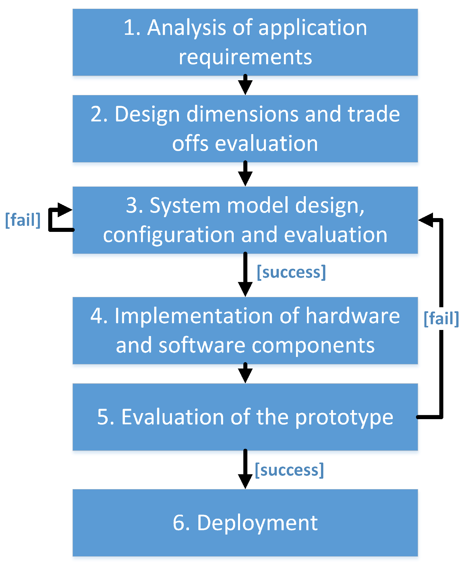
3.1. Design Methodology
- In the first phase, the application is analyzed, and the requirements, desired functionalities, and operating environment get identified.
- The data collected during the first stage are used for evaluating the design dimensions and balancing the respective trade-offs during the second stage.
- The defined design dimensions and functionalities become the input of the third phase. During this phase, the technical requirements are defined, and the system’s architecture, as well as the architectures of the HW and software (SW) components, are chosen. The completion of phase three may require multiple iterations or even result in a return to phase two if it is found that the defined requirements cannot be fulfilled.
- The focus of the fourth phase is on the design and implementation of the new HW and SW components, configuration or modification of the already-existing components and the integration and testing of all the components as a single system.
- Once all the components of the system are implemented and tested, a few nodes are prototyped and deployed in the test environment to test the networking mechanisms and check the performance of the network as a whole. If some problems are detected, the design may return to one of the earlier phases.
- If no problems are detected, the application is deployed and tested on a large scale, and, if it succeeds, it may enter mass production.
- Does the energy become available periodically or randomly?
- How long can the period of energy unavailability last?
- How big can be the fluctuations in the energy?
- Are there any particular trends in energy availability patterns?
- How does the collected energy scales up depending on the position and design dimensions of the device?
3.2. Target Application and Requirements
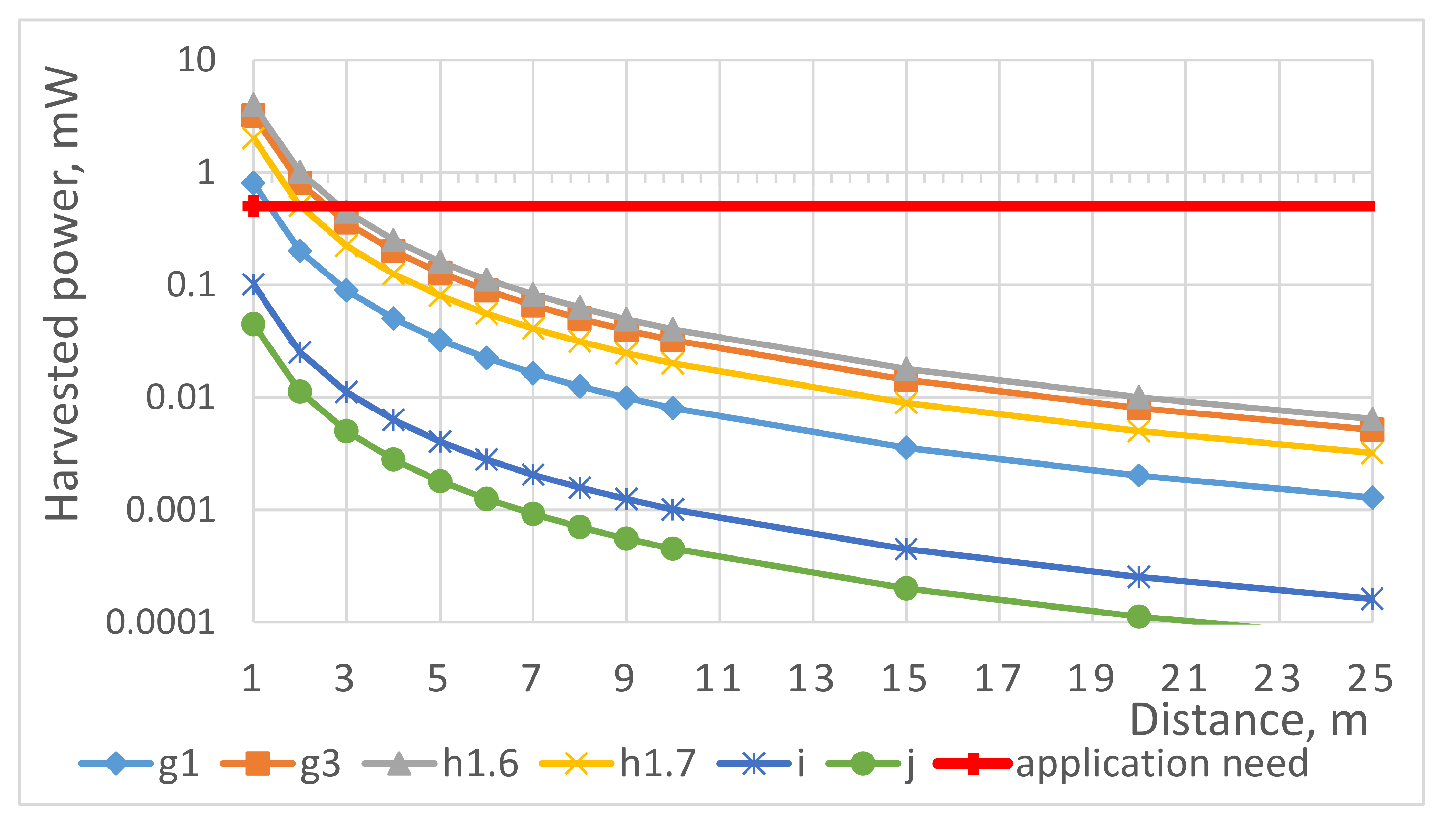
3.3. Feasibility Analysis and Design Dimensions Definition
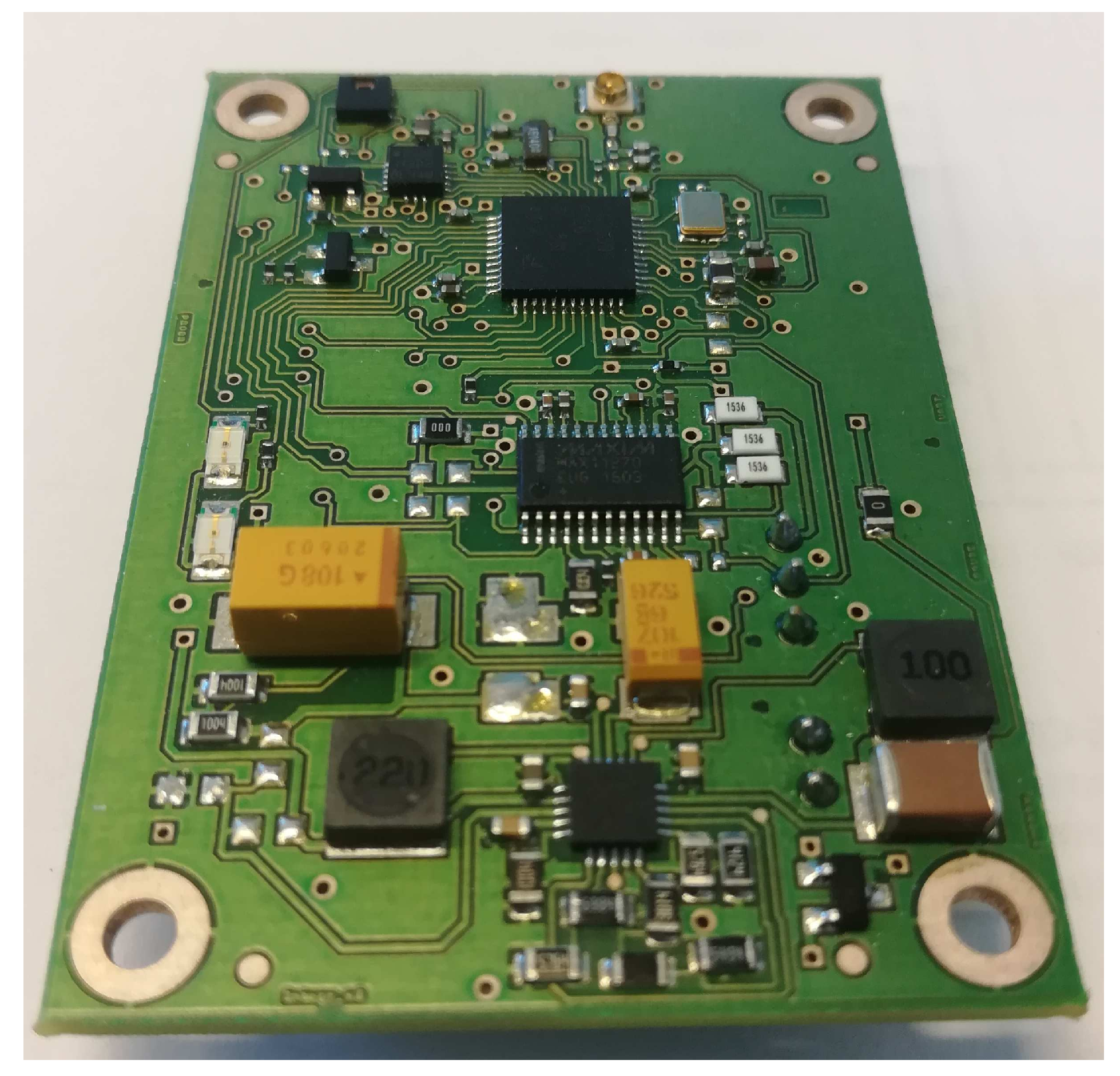
3.4. Implementation and Experimental Validation
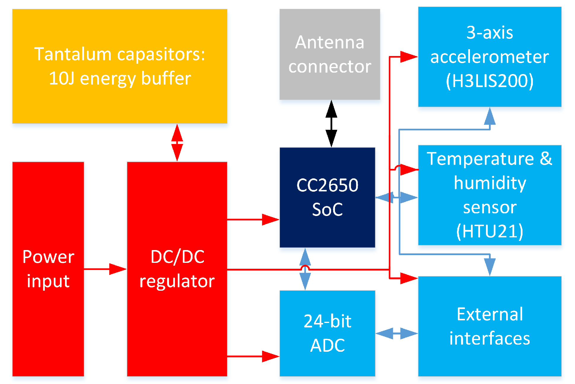
3.4.1. Selection of a Sensor Node
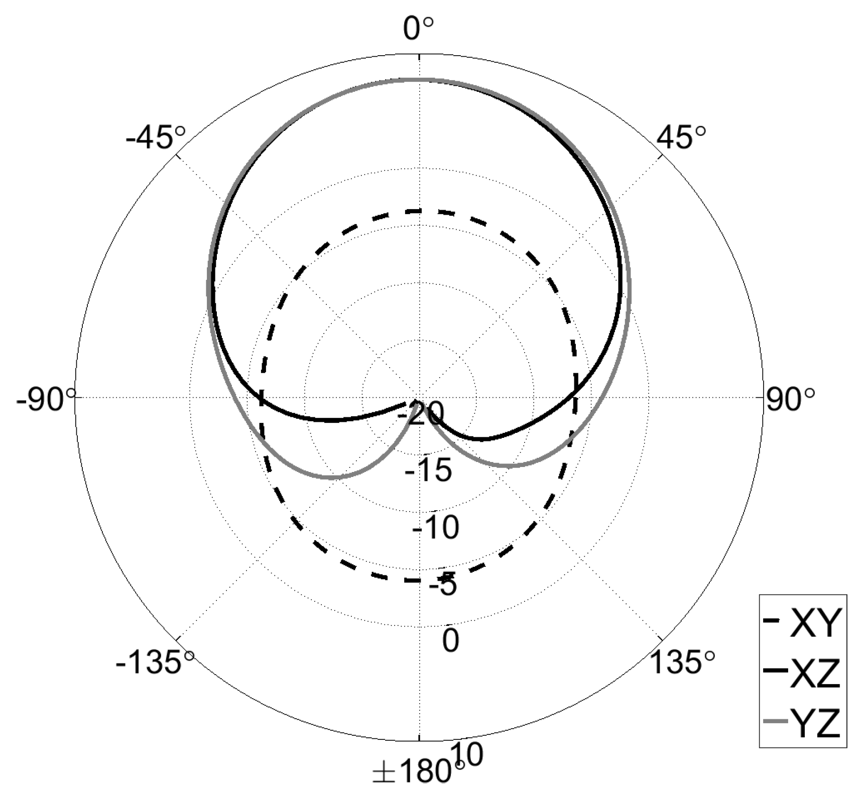
3.4.2. Antennas for RF Energy Transfer
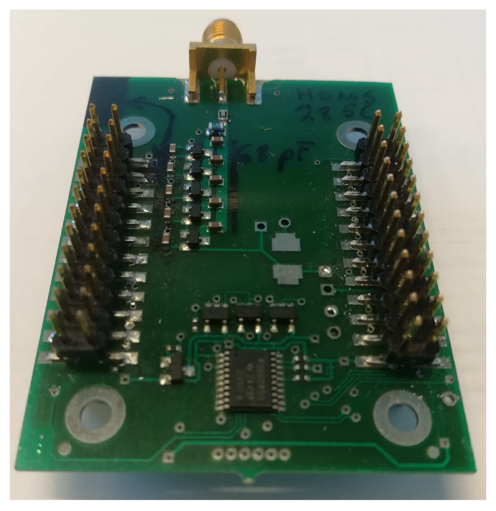
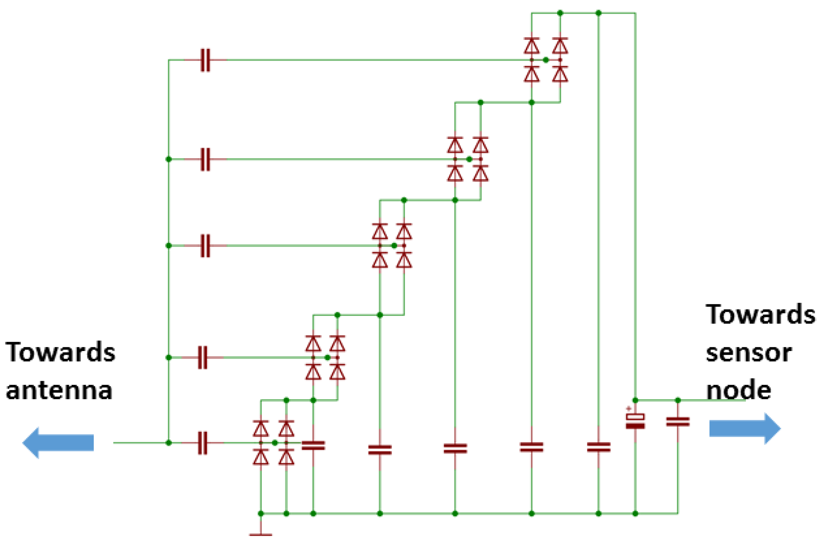
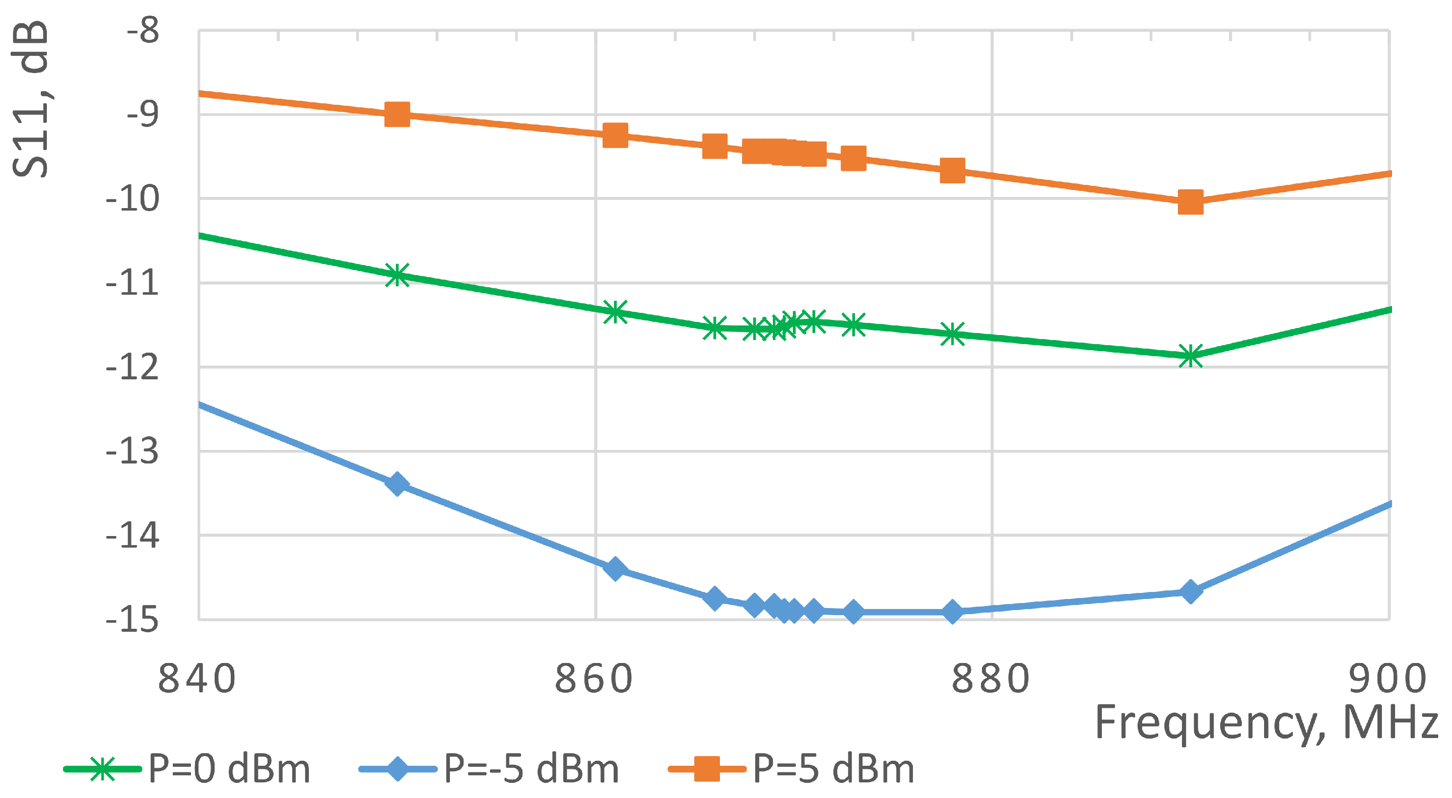
3.4.3. RF–DC Converter
3.4.4. RF Power Source and Gateway
- Operates in 915 MHz US ISM band,
- Has a fixed power level of either 1 or 3 Watt,
- Does not enable duty-cycling,
- Does not permit the connection of external antennas.
3.5. Integration and Evaluation
4. Conclusions
Author Contributions
Funding
Conflicts of Interest
Abbreviations
| BLE | Bluetooth Low Energy |
| DC | Direct Current |
| EIRP | Effective Isotropic Radiated Power |
| FFT | Fast Fourier Transform |
| HW | hardware |
| IEEE | Institute of Electrical and Electronics Engineers |
| ISM | Industrial, Scientific and Medical |
| IoT | Internet of Things |
| LPWAN | Low Power Wide Area Network |
| LTE | Long Term Evolution |
| PCB | Printed Circuit Board |
| RF | Radio Frequency |
| RFID | Radio Frequency Identification |
| SW | software |
| SWIPT | Simultaneous Wireless Information and Power Transfer |
| WPT | Wireless Power Transfer |
| WSN | Wireless Sensor Networks |
References
- Hill, J.L. System Architecture for Wireless Sensor Networks. Ph.D. Thesis, University of California, Berkeley, CA, USA, 2003. [Google Scholar]
- Mikhaylov, K. Plug and Play Reconfigurable Solutions for Heterogeneous IoT. Ph.D. Thesis, University of Oulu, Oulu, Finland, 2018. [Google Scholar]
- Paavola, M.; Leiviska, K. Wireless Sensor Networks in Industrial Automation; INTECH Open Access Publisher: London, UK, 2010. [Google Scholar]
- Setiawan, D.; Aziz, A.A.; Kim, D.I.; Choi, K.W. Experiment, Modeling, and Analysis of Wireless-Powered Sensor Network for Energy Neutral Power Management. IEEE Syst. J. 2018, 12, 381–3392. [Google Scholar] [CrossRef]
- HTU21D(F) RH/T SENSOR IC. Available online: https://www.mouser.fi/pdfdocs/HTU21DF.PDF (accessed on 4 December 2018).
- Datasheet SHTC1 Humidity and Temperature Sensor IC. Available online: https://www.sensirion.com/fileadmin/user_upload/customers/sensirion/Dokumente/0_Datasheets/Humidity/Sensirion_Humidity_Sensors_SHTC1_Datasheet.pdf (accessed on 4 December 2018).
- Datasheet Sensirion SCD30 Sensor Module: CO2, Humidity, and Temperature Sensor. Available online: https://www.sensirion.com/fileadmin/user_upload/customers/sensirion/Dokumente/0_Datasheets/CO2/Sensirion_CO2_Sensors_SCD30_Datasheet.pdf (accessed on 4 December 2018).
- Telaire T6713 Series CO2 Module. Available online: http://www.mouser.com/ds/2/18/AAS-920-634D-Telaire-T6713%20Series-092415-web-1076778.pdf (accessed on 4 December 2018).
- Andreev, S.; Galinina, O.; Pyattaev, A.; Gerasimenko, M.; Tirronen, T.; Torsner, J.; Sachs, J.; Dohler, M.; Koucheryavy, Y. Understanding the IoT connectivity landscape: A contemporary M2M radio technology roadmap. IEEE Commun. Mag. 2015, 53, 32–40. [Google Scholar] [CrossRef]
- Raza, U.; Kulkarni, P.; Sooriyabandara, M. Low Power Wide Area Networks: An Overview. IEEE Commun. Surv. Tutor. 2017, 19, 855–873. [Google Scholar] [CrossRef]
- Valenta, C.R.; Durgin, G.D. Harvesting Wireless Power: Survey of Energy-Harvester Conversion Efficiency in Far-Field, Wireless Power Transfer Systems. IEEE Microw. Mag. 2014, 15, 108–120. [Google Scholar]
- Janhunen, J.; Mikhaylov, K.; Petäjäjärvi, J. Experimental RF-Signal Based Wireless Energy Transmission. In Proceedings of the European Conference on Networks and Communications, Oulu, Finland, 12–15 June 2017; pp. 1–6. [Google Scholar]
- Abdulhadi, A.E.; Denidni, T.A. Self-Powered Multi-Port UHF RFID Tag-Based-Sensor. IEEE J. Freq. Identif. 2017, 1, 115–123. [Google Scholar] [CrossRef]
- Opasjumruskit, K.; Thanthipwan, T.; Sathusen, O.; Sirinamarattana, P.; Gadmanee, P.; Pootarapan, E.; Wongkomet, E.; Thanachayanont, A.; Thamsirianunt, M. Self-powered wireless temperature sensors exploit RFID technology. IEEE Pervasive Comput. 2016, 5, 54–61. [Google Scholar]
- Datasheet PCT100 Powercast High-Function RFID Sensor Tag. Available online: http://www.powercastco.com/wp-content/uploads/2017/07/PCT100-Datasheet-Rev-3.pdf (accessed on 12 December 2018).
- Iannello, F.; Simeone, O.; Spagnolini, U. Energy Management Policies for Passive RFID Sensors with RF-Energy Harvesting. In Proceedings of the IEEE International Conference on Communications, Cape Town, South Africa, 23–27 May 2010; pp. 1–6. [Google Scholar]
- Van Huynh, N.; Hoang, D.T.; Lu, X.; Niyato, D.; Wang, P.; Kim, D.I. Ambient Backscatter Communications: A Contemporary Survey. IEEE Commun. Surv. Tutor. 2018, 20, 2889–2922. [Google Scholar] [CrossRef]
- Powercast, P2110B Data Sheet. Available online: https://www.powercastco.com/wp-content/uploads/ 2016/12/P2110B-Datasheet-Rev-3.pdf (accessed on 4 December 2018).
- Khan, Z.H.N.; Khan, D.; Ahmad, N.; Abbasizadeh, H.; Shah, S.A.A.; Park, Y.J.; Lee, K.Y. 6-Parallel RF energy harvesting rectifier with high power conversion efficiency (PCE) for 5.8 GHz 3 W wireless power transfer. In Proceedings of the IEEE International SoC Design Conference, Seoul, Korea, 5–8 November 2017; pp. 208–209. [Google Scholar]
- Komurasaki, K.M.K.; Hatakeyama, W.; Okamoto, Y.; Minakawa, S.; Suzuki, M.; Shimamura, K.; Mizushima, A.; Fujiwara, K.; Yamaoka, H. Microstrip antenna and rectifier for wireless power transfar at 94 GHz. In Proceedings of the IEEE Wireless Power Transfer Conference, Taipei, Taiwan, 10–12 May 2017; pp. 1–3. [Google Scholar]
- Almohaimeed, A.M.; Yagoub, M.C.E.; Amaya, R.E. A highly efficient power harvester with wide dynamic input power range for 900 MHz wireless power transfer applications. In Proceedings of the 16th Mediterranean Microwave Symposium, Abu Dhabi, United Arab, 14–16 November 2016; pp. 1–4. [Google Scholar]
- Liu, Z.; Guo, Y. Enhanced Dual-Band Ambient RF Energy Harvesting With Ultra-Wide Power Range. IEEE Microw. Wirel. Compon. Lett. 2015, 25, 630–632. [Google Scholar] [CrossRef]
- Sun, H. An Enhanced Rectenna Using Differentially-Fed Rectifier for Wireless Power Transmission. IEEE Antennas Wirel. Propag. Lett. 2016, 15, 32–35. [Google Scholar] [CrossRef]
- Kimionis, J.; Collado, A.; Tentzeris, M.M.; Georgiadis, A. Octave and Decade Printed UWB Rectifiers Based on Nonuniform Transmission Lines for Energy Harvesting. IEEE Trans. Microw. Theory Tech. 2017, 65, 4326–4334. [Google Scholar] [CrossRef]
- Palazzi, V.; Del Prete, M.; Fantuzzi, M. Scavenging for Energy: A Rectenna Design for Wireless Energy Harvesting in UHF Mobile Telephony Bands. IEEE Microw. Mag. 2017, 18, 91–99. [Google Scholar] [CrossRef]
- Awais, Q.; Jin, Y.; Chattha, H.T.; Jamil, M.; Qiang, H.; Khawaja, B.A. A Compact Rectenna System with High Conversion Efficiency for Wireless Energy Harvesting. IEEE Access 2018, 6, 35857–35866. [Google Scholar] [CrossRef]
- Ngo, T.; Huang, A.; Guo, Y.X. Analysis and Design of a Reconfigurable Rectifier Circuit for Wireless Power Transfer. IEEE Trans. Ind. Electron. 2018, in press. [Google Scholar] [CrossRef]
- Shi, Y.; Fan, Y.; Li, Y.; Yang, L.; Wang, M. An Efficient Broadband Slotted Rectenna for Wireless Power Transfer at LTE Band. IEEE Trans. Antennas Propag. 2018, in press. [Google Scholar] [CrossRef]
- Kim, D.; Ingram, M.A.; Smith, W.W., Jr. Efficient far-field radio frequency energy harvesting for passively powered sensor networks. IEEE J. Solid-State Circuits 2008, 43, 1287–1302. [Google Scholar]
- Yi, J.; Ki, W.; Tsui, C. Analysis and design strategy of UHF micro-power CMOS rectifiers for micro-sensor and RFID applications. IEEE Trans. Circuits Syst. 2007, 54, 153–166. [Google Scholar] [CrossRef]
- Scorcioni, S.; Larcher, L.; Bertacchini, A.; Vincetti, L.; Maini, M. An integrated RF energy harvester for UHF wireless powering applications. In Proceedings of the IEEE Wireless Power Transfer Conference, Perugia, Italy, 15–16 May 2013; pp. 92–95. [Google Scholar]
- Curty, J.; Joehl, N.; Dehollain, C.; Declercq, M. Remotely powered addressable UHF RFID integrated system. IEEE J. Solid-State Circuits 2005, 40, 2193–2202. [Google Scholar] [CrossRef]
- Olgun, U.; Chen, C.; Volakis, J. Wireless power harvesting with planar rectennas for 2.45 GHz RFIDs. In Proceedings of the International Symposium on Electromagnetic Theory, Berlin, Germany, 16–19 August 2010; pp. 329–331. [Google Scholar]
- McSpadden, J.; Fan, L.; Chang, K. Design and experiments of a high-conversion-efficiency 5.8-GHz rectenna. IEEE Trans. Microw. Theory Tech. 1998, 46, 1–8. [Google Scholar] [CrossRef]
- Nishida, K.; Taniguchi, Y.; Kawakami, K.; Homma, Y.; Mizutani, H.; Miyazaki, M.; Ikematsu, H.; Shinohara, N. 5.8 GHz high sensitivity rectenna array. In Proceedings of the International Microwave Symposium Series—Innovative Wireless Power Transmission, Kyoto, Japan, 12–13 May 2011; pp. 19–22. [Google Scholar]
- Yoo, T.; Chang, K. Theoretical and experimental development of 10 and 35 GHz rectennas. IEEE Trans. Microw. Theory Tech. 1992, 40, 1–8. [Google Scholar] [CrossRef]
- Collado, A.; Georgiadis, A. 24 GHz substrate integrated waveguide (SIW) rectenna for energy harvesting and wireless power transmission. In Proceedings of the IEEE Microwave Theory and Techniques Society Symposium, Seattle, WA, USA, 2–7 June 2013; pp. 1–3. [Google Scholar]
- Koert, P.; Cha, J. Millimeter wave technology for space power beaming. IEEE Trans. Microw. Theory Tech. 1992, 40, 1251–1258. [Google Scholar] [CrossRef]
- Choi, K.W.; Ginting, L.; Rosyady, P.; Aziz, A.A.; Kim, D.I. Wireless-Powered Sensor Networks: How to Realize. IEEE Trans. Wirel. Commun. 2017, 16, 221–234. [Google Scholar] [CrossRef]
- Choi, K.W.; Rosyady, P.A.; Ginting, L.; Aziz, A.A.; Setiawan, D.; Kim, D.I. Theory and Experiment for Wireless-Powered Sensor Networks: How to Keep Sensors Alive. IEEE Trans. Wirel. Commun. 2018, 17, 430–444. [Google Scholar] [CrossRef]
- Choi, K.W.; Aziz, A.A.; Setiawan, D.; Tran, N.N.; Ginting, L.; Kim, D.I. Distributed Wireless Power Transfer System for Internet-of-Things Devices. IEEE Internet Things J. 2018, 5, 2657–2671. [Google Scholar] [CrossRef]
- Lu, X.; Wang, P.; Niyato, D.; Kim, D.I.; Han, Z. Wireless Networks With RF Energy Harvesting: A Contemporary Survey. IEEE Commun. Surv. Tutor. 2015, 17, 757–789. [Google Scholar] [CrossRef]
- Zhang, R.; Ho, C.K. MIMO broadcasting for simultaneous wireless information and power transfer. IEEE Trans. Wirel. Commun. 2013, 12, 1989–2001. [Google Scholar] [CrossRef]
- Li, B.; Fei, Z.; Chu, Z.; Zhang, Y. Secure Transmission for Heterogeneous Cellular Networks with Wireless Information and Power Transfer. IEEE Syst. J. 2018, in press. [Google Scholar] [CrossRef]
- Zhou, F.; Beaulieu, M.C.; Cheng, J.; Chu, Z.; Wang, Y. Robust Max–Min Fairness Resource Allocation in Sensing-Based Wideband Cognitive Radio With SWIPT: Imperfect Channel Sensing. IEEE Syst. J. 2018, 12, 2361–2372. [Google Scholar] [CrossRef]
- Galinina, O.; Mikhaylov, K.; Huang, K.; Andreev, S.; Koucheryavy, Y. Wirelessly Powered Urban Crowd Sensing over Wearables: Trading Energy for Data. IEEE Wirel. Commun. 2018, 25, 140–149. [Google Scholar] [CrossRef]
- Xu, J.; Liu, L.; Zhang, R. Multiuser MISO Beamforming for Simultaneous Wireless Information and Power Transfer. IEEE Trans. Signal. Process. 2014, 62, 4798–4810. [Google Scholar] [CrossRef]
- Kamalinejad, P.; Mahapatra, C.; Sheng, Z.; Mirabbasi, S.; Leung, V.C.M.; Guan, Y.L. Wireless energy harvesting for the Internet of Things. IEEE Wirel. Commun. Mag. 2015, 53, 102–108. [Google Scholar] [CrossRef]
- He, S.; Xie, K.; Chen, W.; Zhang, D.; Wen, J. Energy-Aware Routing for SWIPT in Multi-Hop Energy-Constrained Wireless Network. IEEE Access 2018, 6, 17996–18008. [Google Scholar] [CrossRef]
- Choi, H.; Shin, W. Slotted ALOHA for Wireless Powered Communication Networks. IEEE Access 2018, 6, 53342–53355. [Google Scholar] [CrossRef]
- Shi, Q.; Xu, W.; Chang, T.; Wang, Y.; Song, E. Joint Beamforming and Power Splitting for MISO Interference Channel With SWIPT: An SOCP Relaxation and Decentralized Algorithm. IEEE Trans. Signal Process. 2014, 62, 6194–6208. [Google Scholar] [CrossRef]
- Lee, S.; Liu, L.; Zhang, R. Collaborative Wireless Energy and Information Transfer in Interference Channel. IEEE Trans. Wirel. Commun. 2015, 14, 545–557. [Google Scholar] [CrossRef]
- Wolf, W. Computers as Components: Principles of Embedded Computing System Design; Elsevier: Burlington, MA, USA, 2000. [Google Scholar]
- Kuorilehto, M.; Kohvakka, M.; Suhonen, J.; Hamalainen, H.; Hannikainen, M.; Hamalainen, T.D. Ultra-Low Energy Wireless Sensor Networks in Practice; John Wiley & Sons: Chichester, UK, 2007. [Google Scholar]
- Mohanty, S.; Gupta, K.K.; Raju, K.S.; Mishra, V.; Kumar, V.; Prasad, P.B. Characterization of wireless accelerometer sensor and its industrial applications. In Proceedings of the 20th National Conference on Communications, Kanpur, India, 28 February–2 March 2014; pp. 1–5. [Google Scholar]
- Fischer, A. Angular-Dependent Radius Measurements at Rotating Objects Using Underdetermined Sensor Systems. IEEE Trans. Instrum. Meas. 2018, 67, 425–430. [Google Scholar] [CrossRef]
- Prochazka, P.; Vanek, F. Non-contact measurement of stationary characteristics of shrouded steam turbine blades under rotation. In Proceedings of the IEEE International Instrumentation and Measurement Technology Conference, Pisa, Italy, 11–14 May 2015; pp. 2084–2088. [Google Scholar]
- Hansen, S.V.; Petersen, J.B.; Jensen, J.J.; Lutzen, M. Performance Monitoring of Ships; Technical University of Denmark: Copenhagen, Denmark, 2012. [Google Scholar]
- Prochaska, M.; Rohrmann, K.; Sandner, M.; Meier, P.; Freund, F. A readout concept for AC-driven xMR sensors in automotive wheel speed applications. In Proceedings of the 9th Latin American Symposium on Circuits & Systems, Puerto Vallarta, Mexico, 25–28 February 2018; pp. 1–4. [Google Scholar]
- ERC Recommendation 70-03, ERC 70-03. Available online: https://www.cept.org/Documents/srd/mg/933/Info_6_ERC_REC_70-03_August_2011 (accessed on 4 December 2018).
- Ficora. Regulation 15 on Collective Frequencies for Licence-Exempt Radio Transmitters and on Their Use. Available online: https://www.finlex.fi/data/normit/32670/MPS_15AM2018M_EN.pdf (accessed on 4 December 2018).
- Solmu Technologies Ltd. Web Page. Available online: http://www.solmutech.com/ (accessed on 4 December 2018).
- Brown, W. The History of Power Transmission by Radio Waves. IEEE Trans. Microw. Theory Tech. 1984, 32, 1230–1242. [Google Scholar] [CrossRef]
- Octopart. Available online: https://octopart.com/search?q=P2110&start=0&manufacturer.displayname=Powercast (accessed on 4 December 2018).
- Lin, S.; Kuo, C.; Lu, S.; Liao, Y. A high-efficiency power management IC with power-aware multi-path rectifier for wide-range RF energy harvesting. In Proceedings of the International Microwave Symposium Series, Honololu, HI, USA, 4–9 June 2017; pp. 304–306. [Google Scholar]
- Mikhaylov, K.; Petajajarvi, J. Design and Implementation of The Plug&Play Enabled Flexible Modular Wireless Sensor and Actuator Network Platform. Asian J. Control 2017, 19, 1392–1412. [Google Scholar]
- POWERCASTER Transmitter. Available online: https://www.powercastco.com/products/powercaster-transmitter/ (accessed on 4 December 2018).


| Peak Efficiency (%) | Input Signal for Peak Efficiency (dBm) | Frequency Band (GHz) | Source |
|---|---|---|---|
| 40 | −10 | 0.25–3 | [24] |
| 65 | 0 | 0.7–1 | [25] |
| 10 | −22.6 | 0.906 | [29] |
| 26.5 | −11.1 | 0.900 | [30] |
| 60 | −3 | 0.915 | [31] |
| 78 | 22 | 0.915 | [21] |
| 60 | 5 | 0.915 | [22] |
| 80 | 17 | 1.0 | [27] |
| 37 | −25.7 | 2.450 | [32] |
| 60 | −5 | 2.450 | [33] |
| 90.6 | 39 | 2.450 | [34] |
| 74.9 | 10.1 | 2.450 | [23] |
| 68 | 5 | 2.450 | [26] |
| 70 | 5 | 2.5 | [28] |
| 23 | −10 | 5.800 | [35] |
| 82 | 17 | 5.800 | [34] |
| 85.5 | 37.8 | 5.800 | [19] |
| 60 | 21.5 | 10.000 | [36] |
| 4.5 | −2 | 25.700 | [37] |
| 70 | 7.7 | 35.000 | [38] |
| 38 | 20.2 | 94.000 | [20] |
| Sensor Type | Consumption min | Consumption max |
|---|---|---|
| Movement | ||
| Acclerometers | dozens | hundreds |
| Gyroscopes | units mW | dozens mW |
| Environmental Conditions | ||
| Ambient temperature | units | hundreds |
| Ambient pressure | dozens | dozens |
| Ambient humidity | units | hundreds |
| Ambient light (incl. UV) | dozens | units mW |
| Air quality | dozens | hundreds mW |
| Gas presence | hundreds | hundreds mW |
| Dust (optical) | dozens mW | dozens mW |
| Smoke (optical) | hundreds | units mW |
| Presence | ||
| Magnetic/compass | hundreds | units mW |
| Touch | dozens | hundreds |
| Physical Conditions | ||
| Heart rate | units mW | dozens mW |
| Gestures (optical) | units mW | dozens mW |
| Other | ||
| Audio | hundreds | dozens mW |
| Video | dozens mW | hundreds mW |
| Subband [ERC 70-03] | Frequency (MHz) | Effective Radiated Power (mW/dBm) | Duty Cycle (%) |
|---|---|---|---|
| g1 | 433.050–434.790 | ≤25/14 | |
| g2 | 433.050–434.790 | ≤1/0(−13 dBm/10 kHz) | No restriction |
| g3 | 433.040–434.790 | ≤10/10 | No restriction |
| h1.1–1.3 | 863.000–870.000 | ≤25/14 | ≤0.1 |
| h1.4 | 868.000–868.600 | ≤25/14 | ≤1 |
| h1.5 | 868.700–869.200 | ≤25/14 | ≤0.1 |
| h1.6 | 869.400–869.650 | ≤500/27 | ≤10 |
| h1.7 | 869.700–870.000 | ≤5/7 | No restriction |
| h1.7 | 869.700–870.000 | ≤25/14 | ≤1 |
| h2 | 870.700–873.000 | ≤25/14 | ≤1 |
| i | 2400.000–2483.500 | ≤10/10 (EIRP) | No restriction |
| j | 5725.000–5875.000 | ≤25/14 (EIRP) | No restriction |
| Received Power | Power after DC | Max Voltage (V) | Efficiency (%) |
|---|---|---|---|
| (dBm/mW) | Conversion (mW) | ||
| 5/10.00 | 2.04 | 4.12 | 20 |
| 0/1.00 | 0.59 | 2.21 | 59 |
| −5/0.32 | 0.16 | 1.15 | 51 |
| −10/0.10 | 0.038 | 0.56 | 38 |
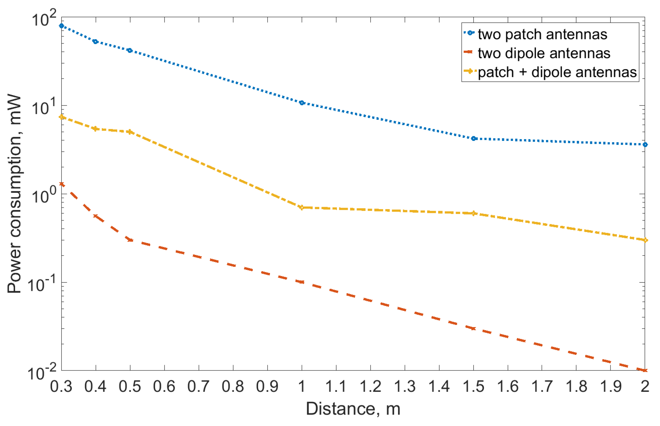
| Distance (m) | Patch (mW) | Dipole (mW) | Patch + Dipole (mW) |
|---|---|---|---|
| 2 | 3.6 | 0.01 | 0.30 |
| 1.5 | 4.2 | 0.03 | 0.60 |
| 1 | 10.7 | 0.10 | 0.70 |
| 0.5 | 41.7 | 0.30 | 5.00 |
| 0.4 | 52.5 | 0.56 | 5.40 |
| 0.3 | 79.40 | 1.30 | 7.40 |
© 2018 by the authors. Licensee MDPI, Basel, Switzerland. This article is an open access article distributed under the terms and conditions of the Creative Commons Attribution (CC BY) license (http://creativecommons.org/licenses/by/4.0/).
Share and Cite
Janhunen, J.; Mikhaylov, K.; Petäjäjärvi, J.; Sonkki, M. Wireless Energy Transfer Powered Wireless Sensor Node for Green IoT: Design, Implementation and Evaluation. Sensors 2019, 19, 90. https://doi.org/10.3390/s19010090
Janhunen J, Mikhaylov K, Petäjäjärvi J, Sonkki M. Wireless Energy Transfer Powered Wireless Sensor Node for Green IoT: Design, Implementation and Evaluation. Sensors. 2019; 19(1):90. https://doi.org/10.3390/s19010090
Chicago/Turabian StyleJanhunen, Janne, Konstantin Mikhaylov, Juha Petäjäjärvi, and Marko Sonkki. 2019. "Wireless Energy Transfer Powered Wireless Sensor Node for Green IoT: Design, Implementation and Evaluation" Sensors 19, no. 1: 90. https://doi.org/10.3390/s19010090
APA StyleJanhunen, J., Mikhaylov, K., Petäjäjärvi, J., & Sonkki, M. (2019). Wireless Energy Transfer Powered Wireless Sensor Node for Green IoT: Design, Implementation and Evaluation. Sensors, 19(1), 90. https://doi.org/10.3390/s19010090