A Microelectrode Array with Reproducible Performance Shows Loss of Consistency Following Functionalization with a Self-Assembled 6-Mercapto-1-hexanol Layer

 ,
, 
 , and
, and 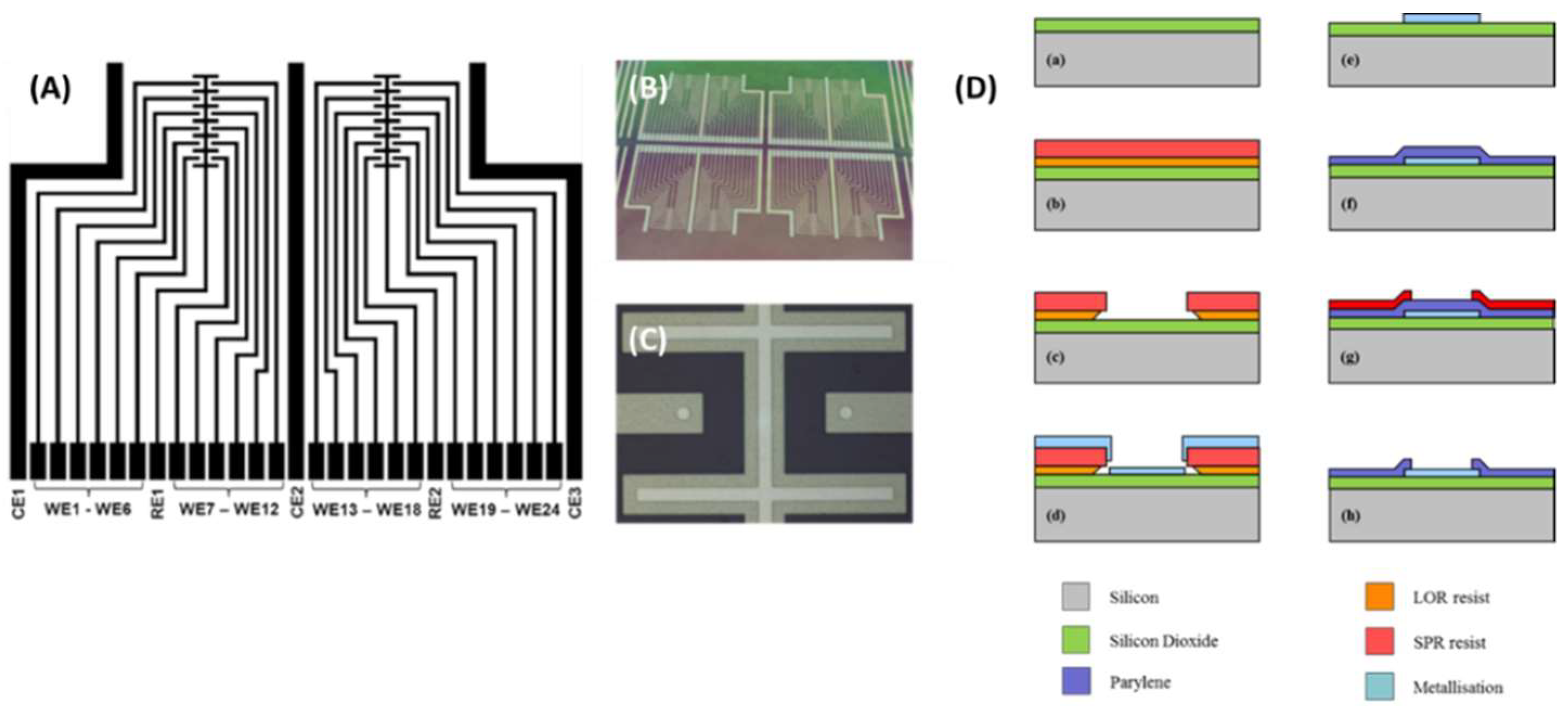
Abstract
1. Introduction
2. Materials and Methods
2.1. Microfabrication of Electrode Devices
2.2. Electrochemical Measurements
2.3. Plating of Silver Reference Electrode and Electrode Cleaning
3. Results and Discussion
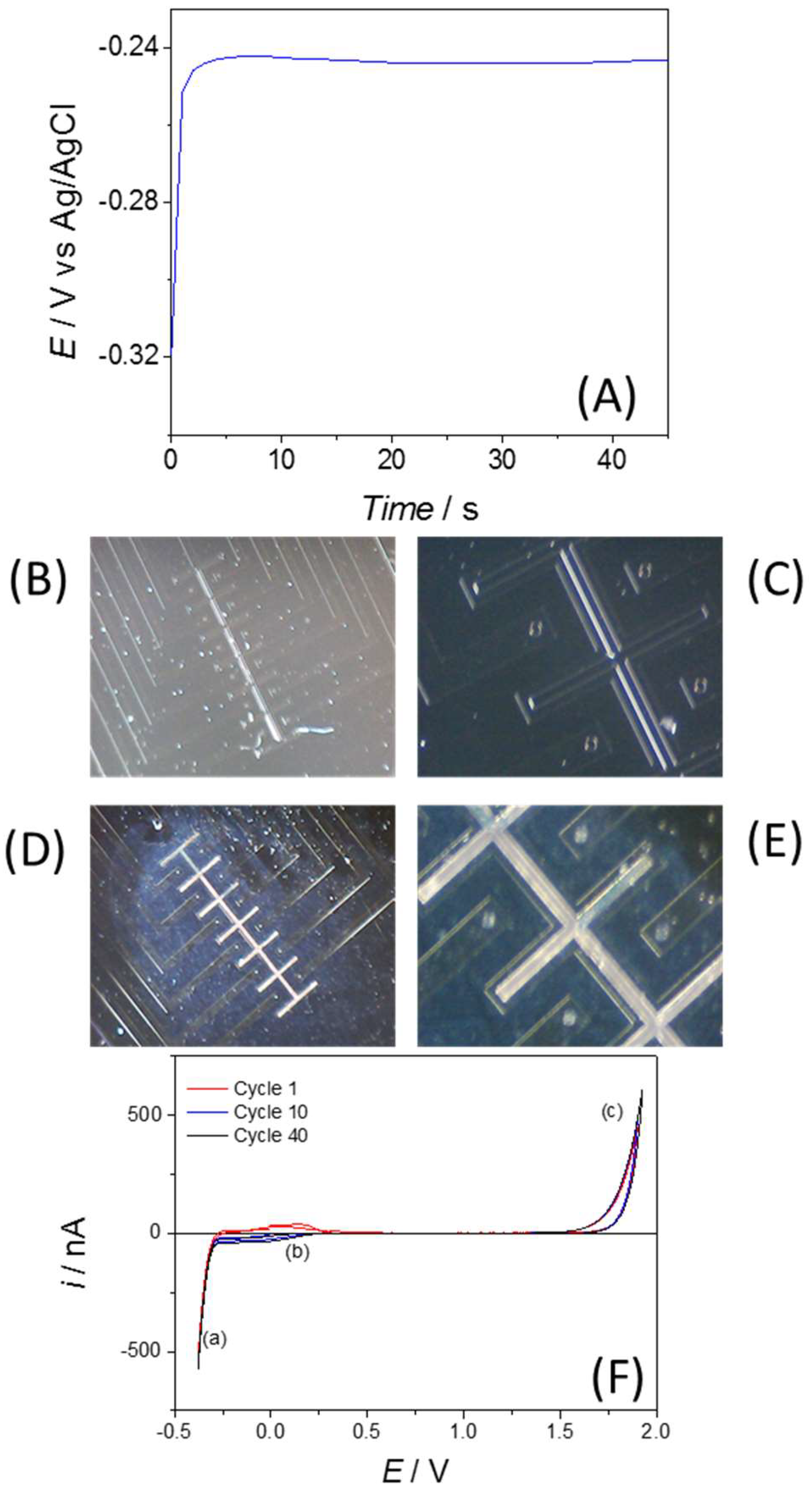
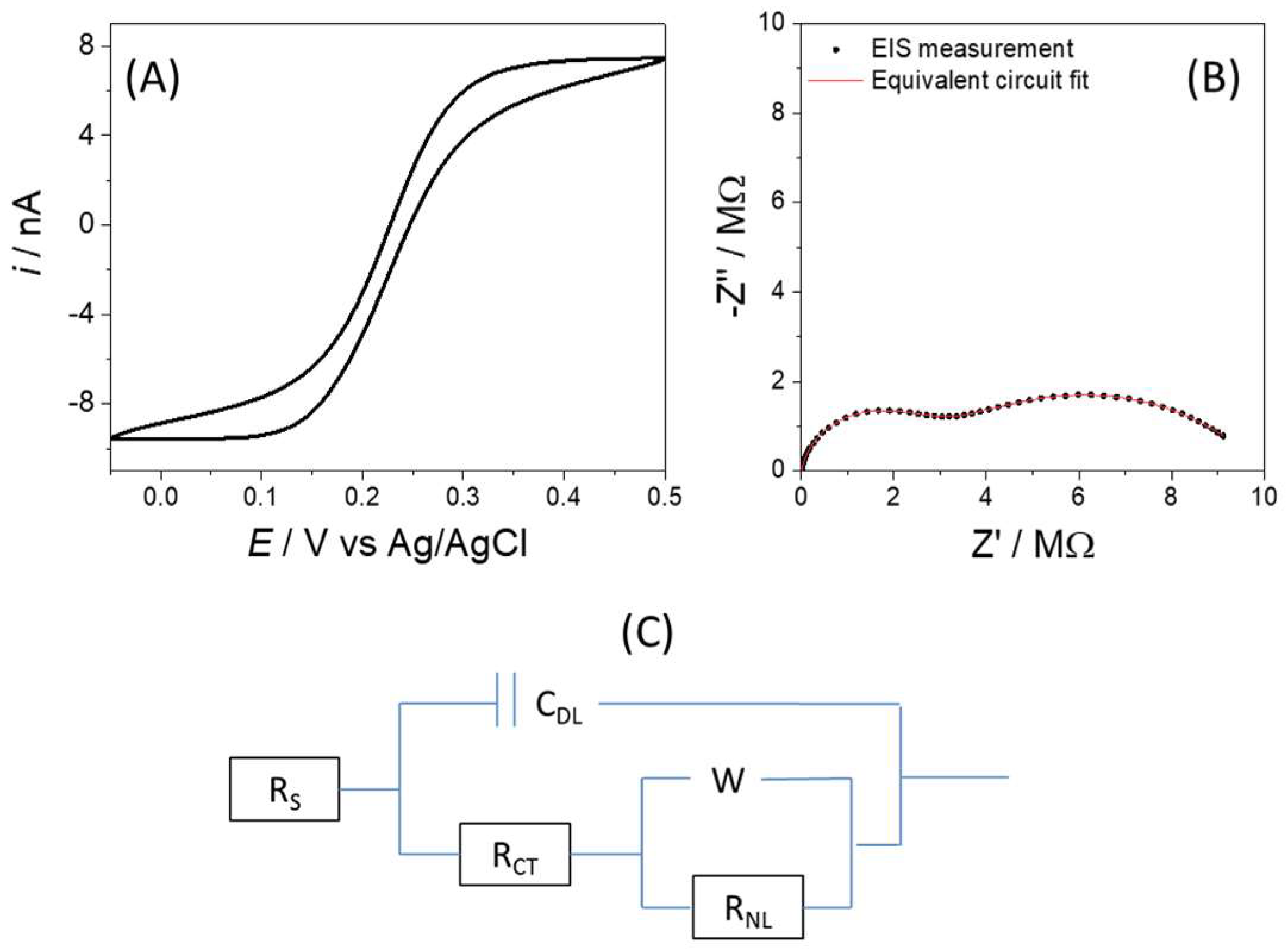
3.1. Electrochemical Characterisation of a 50 µM Disc from the Array
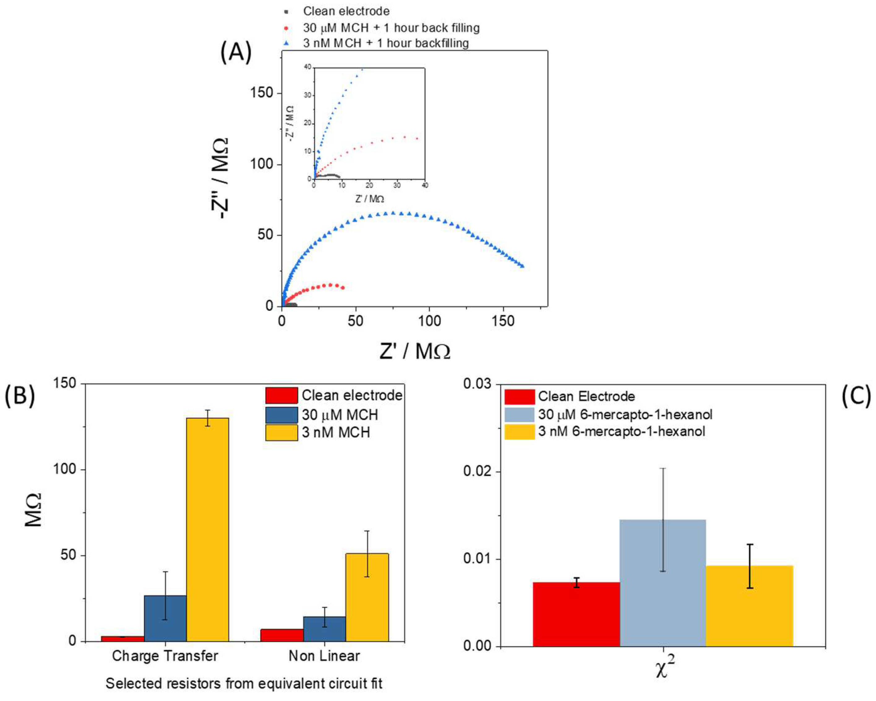
3.2. Electrochemical Response Following Functionalisation with 6-Mercapto-1-hexanol (MCH)
Cyclic Voltammetry
3.3. Electrochemical Impedance Spectroscopy
3.4. Attempts to Improve Consistency of the Chemical Modification of Sensor Surface
4. Conclusions
Author Contributions
Funding
Acknowledgments
Conflicts of Interest
References
- Corrigan, D.K.; Whitcombe, M.J.; McCrossen, S.; Piletsky, S. Reichardt’s Dye and Its Reactions with the Alkylating Agents 4-Chloro-1-Butanol, Ethyl Methanesulfonate, 1-Bromobutane and Fast Red B—A Potentially Useful Reagent for the Detection of Genotoxic Impurities in Pharmaceuticals. J. Pharm. Pharmacol. 2009, 61, 533–537. [Google Scholar] [CrossRef] [PubMed]
- Corrigan, D.K.; Salton, N.A.; Preston, C.; Piletsky, S. Towards the Development of a Rapid, Portable, Surface Enhanced Raman Spectroscopy Based Cleaning Verification System for the Drug Nelarabine. J. Pharm. Pharmacol. 2010, 62, 1195–1200. [Google Scholar] [CrossRef] [PubMed]
- Mutilba, U.; Gomez-Acedo, E.; Kortaberria, G.; Olarra, A.; Yagüe-Fabra, J.A. Traceability of on-Machine Tool Measurement: A Review. Sensors 2017, 17, 1605. [Google Scholar] [CrossRef] [PubMed]
- Zhu, X.-S.; Gao, C.; Choi, J.-W.; Bishop, P.L.; Ahn, C.H. On-Chip Generated Mercury Microelectrode for Heavy Metal Ion Detection. Lab Chip 2005, 5, 212–217. [Google Scholar] [CrossRef] [PubMed]
- Li, Z.; Deen, M.J.; Kumar, S.; Selvaganapathy, P.R. Raman Spectroscopy for in-Line Water Quality Monitoring—Instrumentation and Potential. Sensors 2014, 14, 17275–17303. [Google Scholar] [CrossRef] [PubMed]
- Anandhakumar, S.; Mathiyarasu, J.; Phani, K.L.N. In Situ Bismuth Film Modified Carbon Fiber Microelectrode for Nanomolar Detection of Cadmium and Lead. Indian J. Chem. Sect. A Inorg. Phys. Theor. Anal. Chem. 2012, 51, 699–703. [Google Scholar]
- Tung, T.T.; Nine, M.J.; Krebsz, M.; Pasinszki, T.; Coghlan, C.J.; Tran, D.N.H.; Losic, D. Recent Advances in Sensing Applications of Graphene Assemblies and Their Composites. Adv. Funct. Mater. 2017, 27, 1–57. [Google Scholar] [CrossRef]
- Moschou, D.; Greathead, L.; Pantelidis, P.; Kelleher, P.; Morgan, H.; Prodromakis, T. Amperometric IFN-γ Immunosensors with Commercially Fabricated PCB Sensing Electrodes. Biosens. Bioelectron. 2016, 86, 805–810. [Google Scholar] [CrossRef] [PubMed]
- Wan, Y.; Su, Y.; Zhu, X.; Liu, G.; Fan, C. Development of Electrochemical Immunosensors towards Point of Care Diagnostics. Biosens. Bioelectron. 2013, 47, 1–11. [Google Scholar] [CrossRef] [PubMed]
- Peng, K.; Xie, P.; Yang, Z.H.; Yuan, R.; Zhang, K. Highly Sensitive Electrochemical Nuclear Factor Kappa B Aptasensor Based on Target-Induced Dual-Signal Ratiometric and Polymerase-Assisted Protein Recycling Amplification Strategy. Biosens. Bioelectron. 2018, 102, 282–287. [Google Scholar] [CrossRef] [PubMed]
- Pasinszki, T.; Krebsz, M.; Tung, T.T.; Losic, D. Carbon Nanomaterial Based Biosensors for Non-Invasive Detection of Cancer and Disease Biomarkers for Clinical Diagnosis. Sensors 2017, 17, 1919. [Google Scholar] [CrossRef] [PubMed]
- Forster, R.J. Microelectrodes: New Dimensions in Electrochemistry. Chem. Soc. Rev. 1994, 23, 289–297. [Google Scholar] [CrossRef]
- Heinze, B.J. Ultramicroelectrodes in Electrochemistry. Agnew. Chem. Int. Ed. 1993, 32, 1268–1288. [Google Scholar] [CrossRef]
- Compton, R.G.; Huang, X.; Mahony, A.M.O.; Compton, R.G. Microelectrode Arrays for Electrochemistry: Approaches to Fabrication. Small 2009, 5, 776–788. [Google Scholar]
- Corrigan, D.K.; Blair, E.O.; Terry, J.G.; Walton, A.J.; Mount, A.R. Enhanced Electroanalysis in Lithium Potassium Eutectic (LKE) Using Microfabricated Square Microelectrodes. Anal. Chem. 2014, 86, 11342–11348. [Google Scholar] [CrossRef] [PubMed]
- Corrigan, D.K.; Elliott, J.P.; Blair, E.O.; Reeves, S.J.; Schmüser, I.; Walton, A.J.; Mount, A.R. Advances in Electroanalysis, Sensing and Monitoring in Molten Salts. Faraday Discuss. 2016, 190, 351–366. [Google Scholar] [CrossRef] [PubMed]
- Blair, E.O.; Corrigan, D.K.; Terry, J.G.; Mount, A.R.; Walton, A.J. Development and Optimization of Durable Microelectrodes for Quantitative Electroanalysis in Molten Salt. J. Microelectromech. Syst. 2015, 24, 1346–1354. [Google Scholar] [CrossRef]
- Temiz, Y.; Ferretti, A.; Leblebicib, Y.; Guiducci, C. A comparative study on fabrication techniques for on chip microelectrodes. Lab. Chip. 2012, 4920–4928. [Google Scholar] [CrossRef] [PubMed]
- Wang, J. Electrochemical Nucleic Acid Biosensors. Anal. Chim. Acta 2002, 469, 63–71. [Google Scholar] [CrossRef]
- Park, J.-Y.; Park, S.-M. DNA Hybridization Sensors Based on Electrochemical Impedance Spectroscopy as a Detection Tool. Sensors 2009, 9, 9513–9532. [Google Scholar] [CrossRef] [PubMed]
- Lisdat, F.; Schäfer, D. The Use of Electrochemical Impedance Spectroscopy for Biosensing. Anal. Bioanal. Chem. 2008, 391, 1555–1567. [Google Scholar] [CrossRef] [PubMed]
- Corrigan, D.K.; Schulze, H.; Henihan, G.; Hardie, A.; Ciani, I.; Giraud, G.; Terry, J.G.; Walton, A.J.; Pethig, R.; Ghazal, P.; et al. Development of a PCR-Free Electrochemical Point of Care Test for Clinical Detection of Methicillin Resistant Staphylococcus Aureus (MRSA). Analyst 2013, 138, 6997–7005. [Google Scholar] [CrossRef] [PubMed]
- Corrigan, D.K.; Schulze, H.; Ciani, I.; Henihan, G.; Mount, A.R.; Bachmann, T.T. Improving Performance of a Rapid Electrochemical MRSA Assay: Optimisation of Assay Conditions to Achieve Enhanced Discrimination of Clinically Important DNA Sequences under Ambient Conditions. J. Electroanal. Chem. 2017, 786, 58–62. [Google Scholar] [CrossRef]
- Riedel, M.; Kartchemnik, J.; Schöning, M.J.; Lisdat, F. Impedimetric DNA Detection-Steps Forward to Sensorial Application. Anal. Chem. 2014, 86, 7867–7874. [Google Scholar] [CrossRef] [PubMed]
- Zhu, B.; Travas-Sejdic, J. PNA versus DNA in Electrochemical Gene Sensing Based on Conducting Polymers: Study of Charge and Surface Blocking Effects on the Sensor Signal. Analyst 2018, 143, 687–694. [Google Scholar] [CrossRef] [PubMed]
- Li, P.Q.; Piper, A.; Schmueser, I.; Mount, A.R.; Corrigan, D.K. Impedimetric Measurement of DNA–DNA Hybridisation Using Microelectrodes with Different Radii for Detection of Methicillin Resistant Staphylococcus Aureus (MRSA). Analyst 2017, 142, 1946–1952. [Google Scholar] [CrossRef] [PubMed]
- Ianeselli, L.; Grenci, G.; Callegari, C.; Tormen, M.; Casalis, L. Development of Stable and Reproducible Biosensors Based on Electrochemical Impedance Spectroscopy: Three-Electrode versus Two-Electrode Setup. Biosens. Bioelectron. 2014, 55, 1–6. [Google Scholar] [CrossRef] [PubMed]
- Woodvine, H.L.; Terry, J.G.; Walton, A.J.; Mount, A.R. The Development and Characterisation of Square Microfabricated Electrode Systems. Analyst 2010, 135, 1058–1065. [Google Scholar] [CrossRef] [PubMed]
- Sheffer, M.; Vivier, V.; Mandler, D. Self-Assembled Monolayers on Au Microelectrodes. Electrochem. Commun. 2007, 9, 2827–2832. [Google Scholar] [CrossRef]
- Konopka, S.J.; McDuffie, B. Diffusion Coefficients of Ferri- and Ferrocyanide Ions in Aqueous Media, Using Twin-Electrode Thin-Layer Electrochemistry. Anal. Chem. 1970, 42, 1741–1746. [Google Scholar] [CrossRef]
- Kadara, R.O.; Jenkinson, N.; Banks, C.E. Characterisation of Commercially Available Electrochemical Sensing Platforms. Sens. Actuators B Chem. 2009, 138, 556–562. [Google Scholar] [CrossRef]
- Sosna, M.; Denuault, G.; Pascal, R.W.; Prien, R.D.; Mowlem, M. Development of a Reliable Microelectrode Dissolved Oxygen Sensor. Sens. Actuators B Chem. 2007, 123, 344–351. [Google Scholar] [CrossRef]
- Rahman, H.; Ryall, J.; Davis, J.J.; Bueno, P.R. A Dielectric Model of Self-Assembled Monolayer Interfaces by Capacitive Spectroscopy. Langmuir 2012, 28, 9689–9699. [Google Scholar]
- Terry, J.G.; Schmüser, I.; Underwood, I.; Corrigan, D.K.; Freeman, N.J.; Bunting, A.S.; Mount, A.R.; Walton, A.J. Nanoscale Electrode Arrays Produced with Microscale Lithographic Techniques for Use in Biomedical Sensing Applications. IET Nanobiotechnol. 2013, 7, 125–134. [Google Scholar] [CrossRef] [PubMed]


© 2018 by the authors. Licensee MDPI, Basel, Switzerland. This article is an open access article distributed under the terms and conditions of the Creative Commons Attribution (CC BY) license (http://creativecommons.org/licenses/by/4.0/).
Share and Cite
Corrigan, D.K.; Vezza, V.; Schulze, H.; Bachmann, T.T.; Mount, A.R.; Walton, A.J.; Terry, J.G. A Microelectrode Array with Reproducible Performance Shows Loss of Consistency Following Functionalization with a Self-Assembled 6-Mercapto-1-hexanol Layer. Sensors 2018, 18, 1891. https://doi.org/10.3390/s18061891
Corrigan DK, Vezza V, Schulze H, Bachmann TT, Mount AR, Walton AJ, Terry JG. A Microelectrode Array with Reproducible Performance Shows Loss of Consistency Following Functionalization with a Self-Assembled 6-Mercapto-1-hexanol Layer. Sensors. 2018; 18(6):1891. https://doi.org/10.3390/s18061891
Chicago/Turabian StyleCorrigan, Damion K., Vincent Vezza, Holger Schulze, Till T. Bachmann, Andrew R. Mount, Anthony J. Walton, and Jonathan G. Terry. 2018. "A Microelectrode Array with Reproducible Performance Shows Loss of Consistency Following Functionalization with a Self-Assembled 6-Mercapto-1-hexanol Layer" Sensors 18, no. 6: 1891. https://doi.org/10.3390/s18061891
APA StyleCorrigan, D. K., Vezza, V., Schulze, H., Bachmann, T. T., Mount, A. R., Walton, A. J., & Terry, J. G. (2018). A Microelectrode Array with Reproducible Performance Shows Loss of Consistency Following Functionalization with a Self-Assembled 6-Mercapto-1-hexanol Layer. Sensors, 18(6), 1891. https://doi.org/10.3390/s18061891