Design and Performance of a 1 ms High-Speed Vision Chip with 3D-Stacked 140 GOPS Column-Parallel PEs †

Abstract
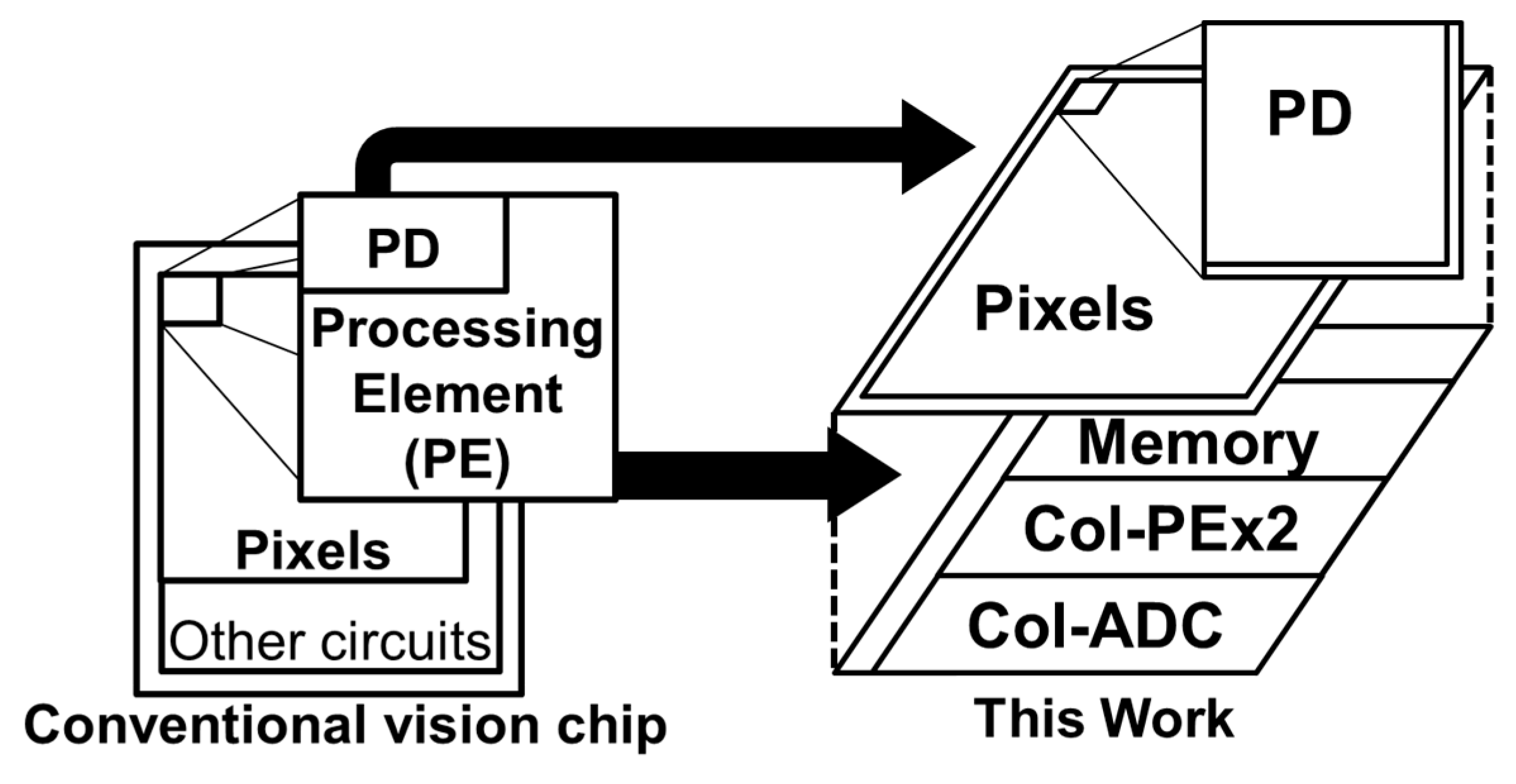
1. Introduction
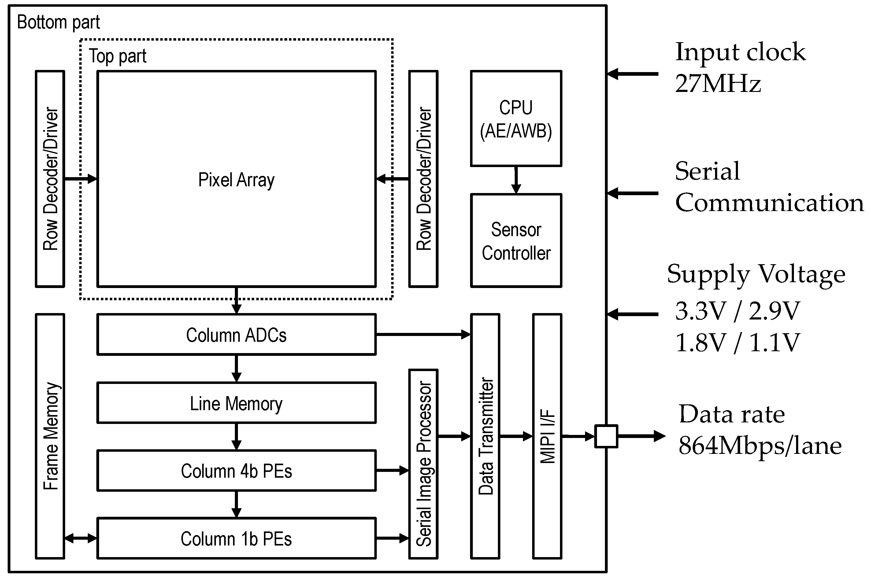
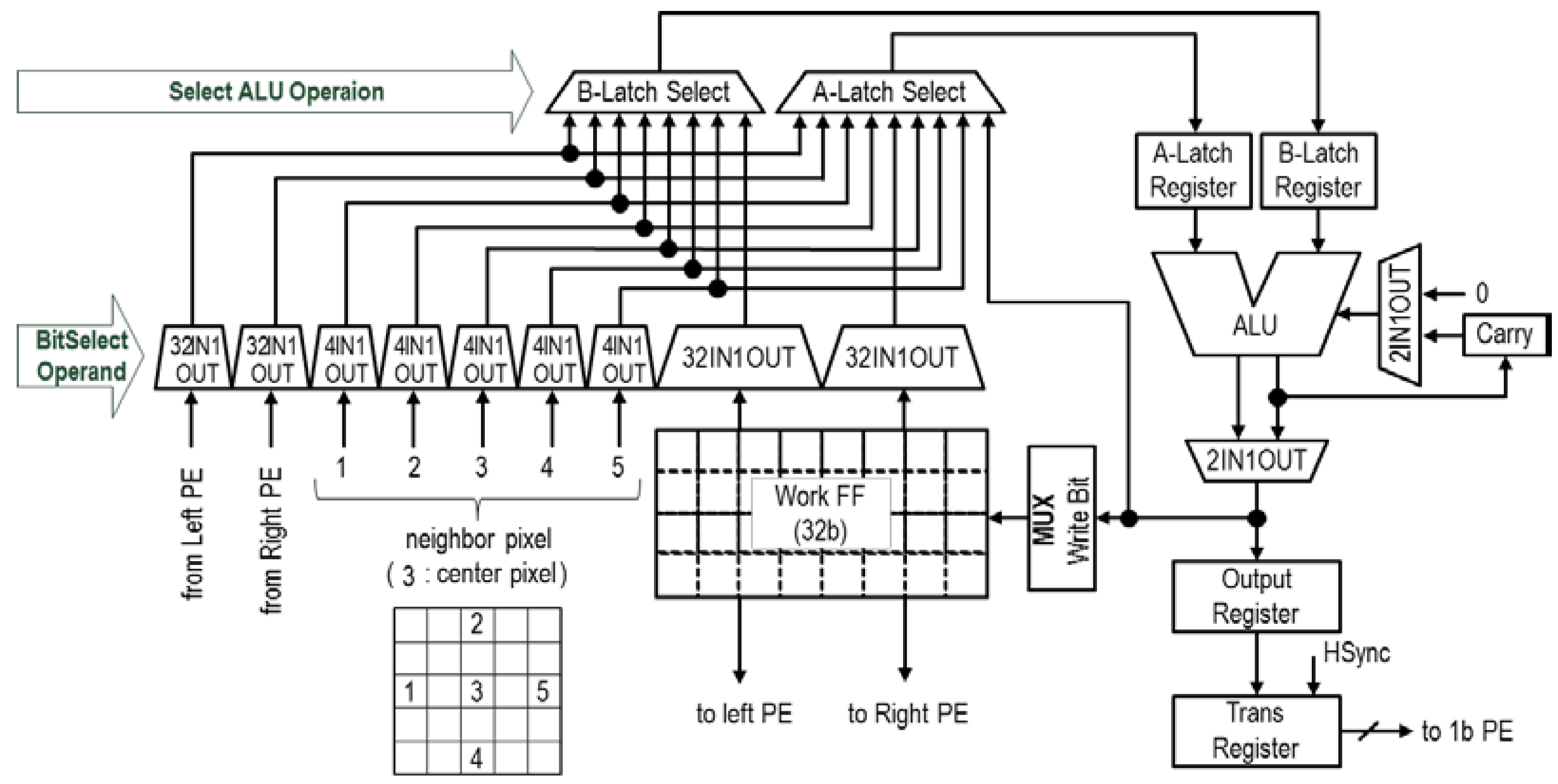
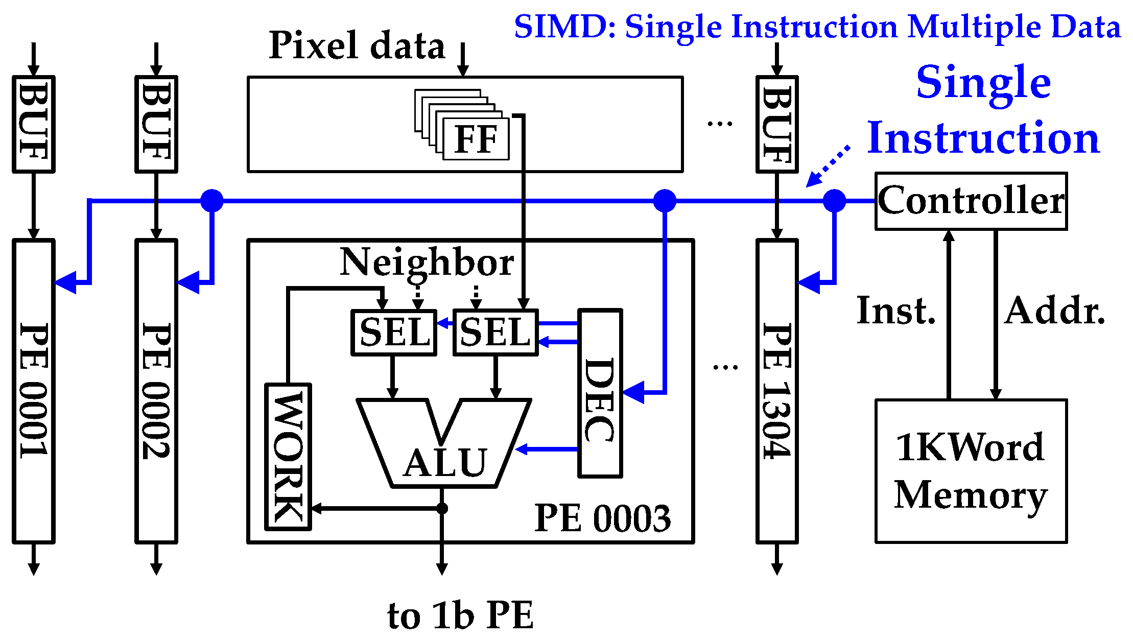
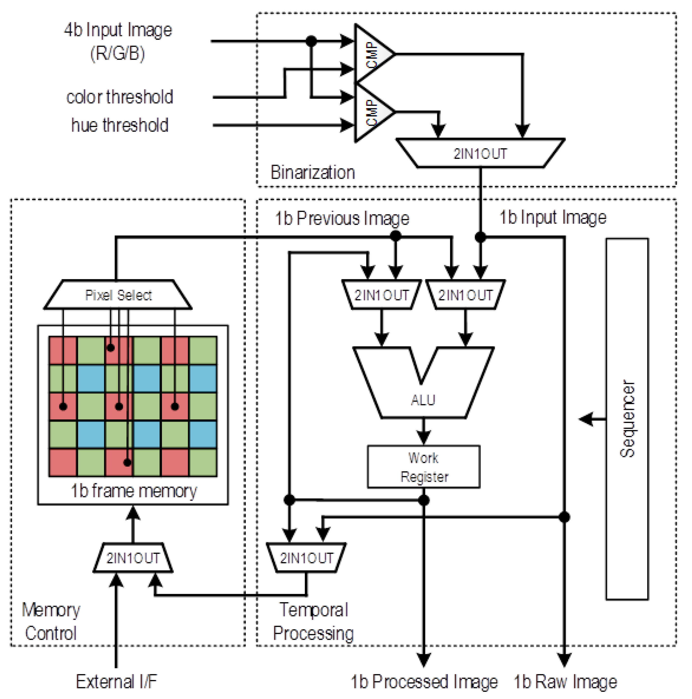
2. Materials and Methods
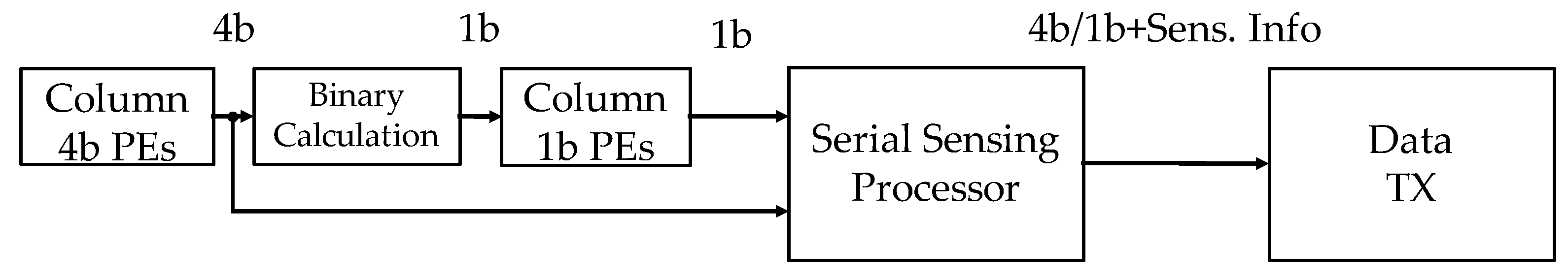
3. Results
4. Experimental Results
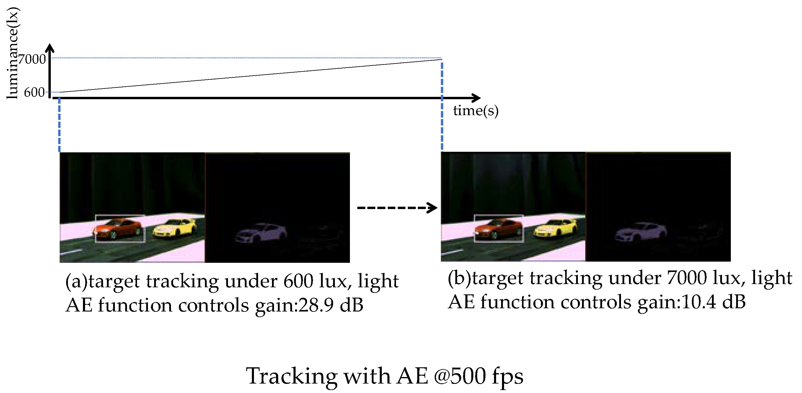
4.1. Auto Adjusting Function Results
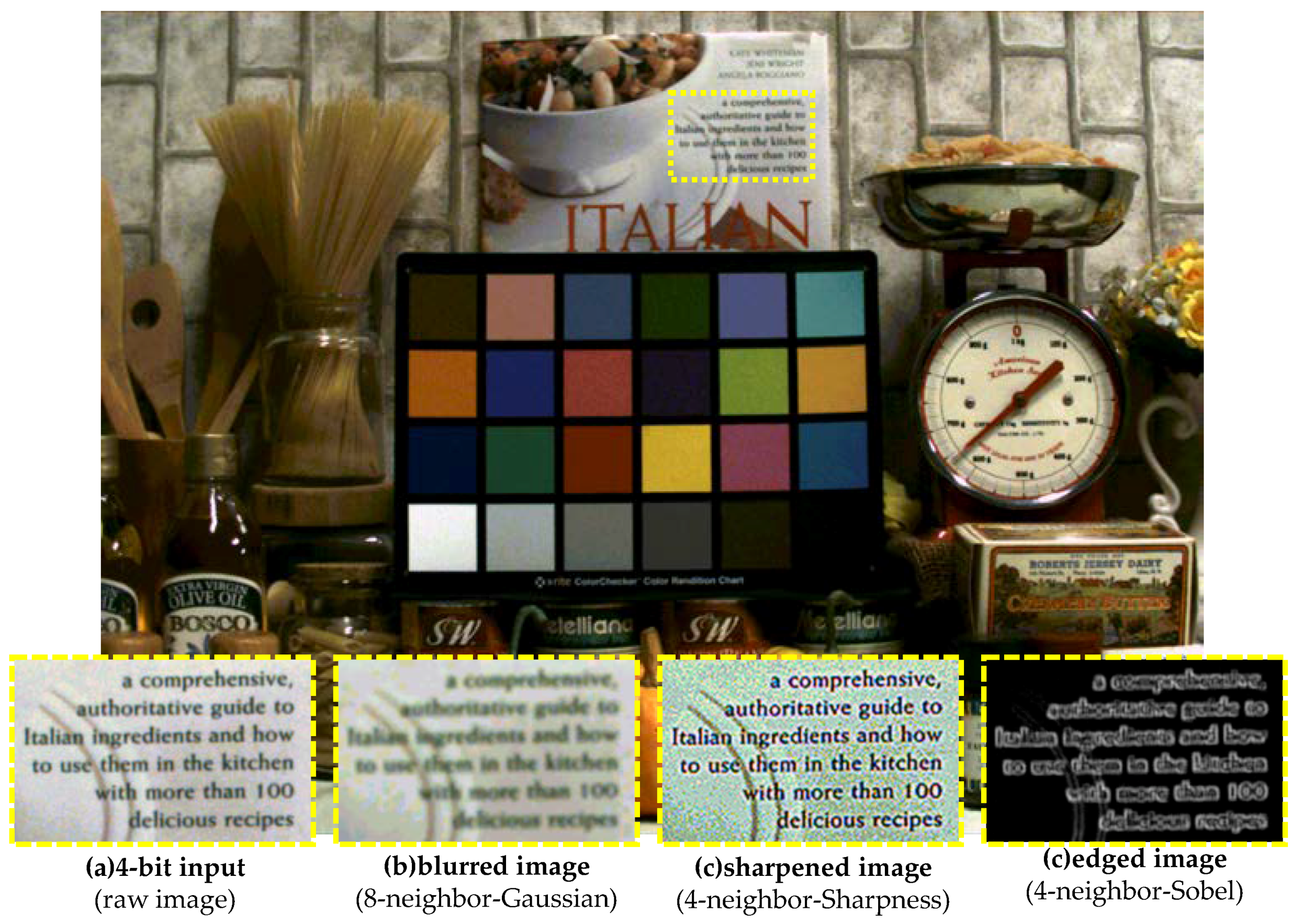
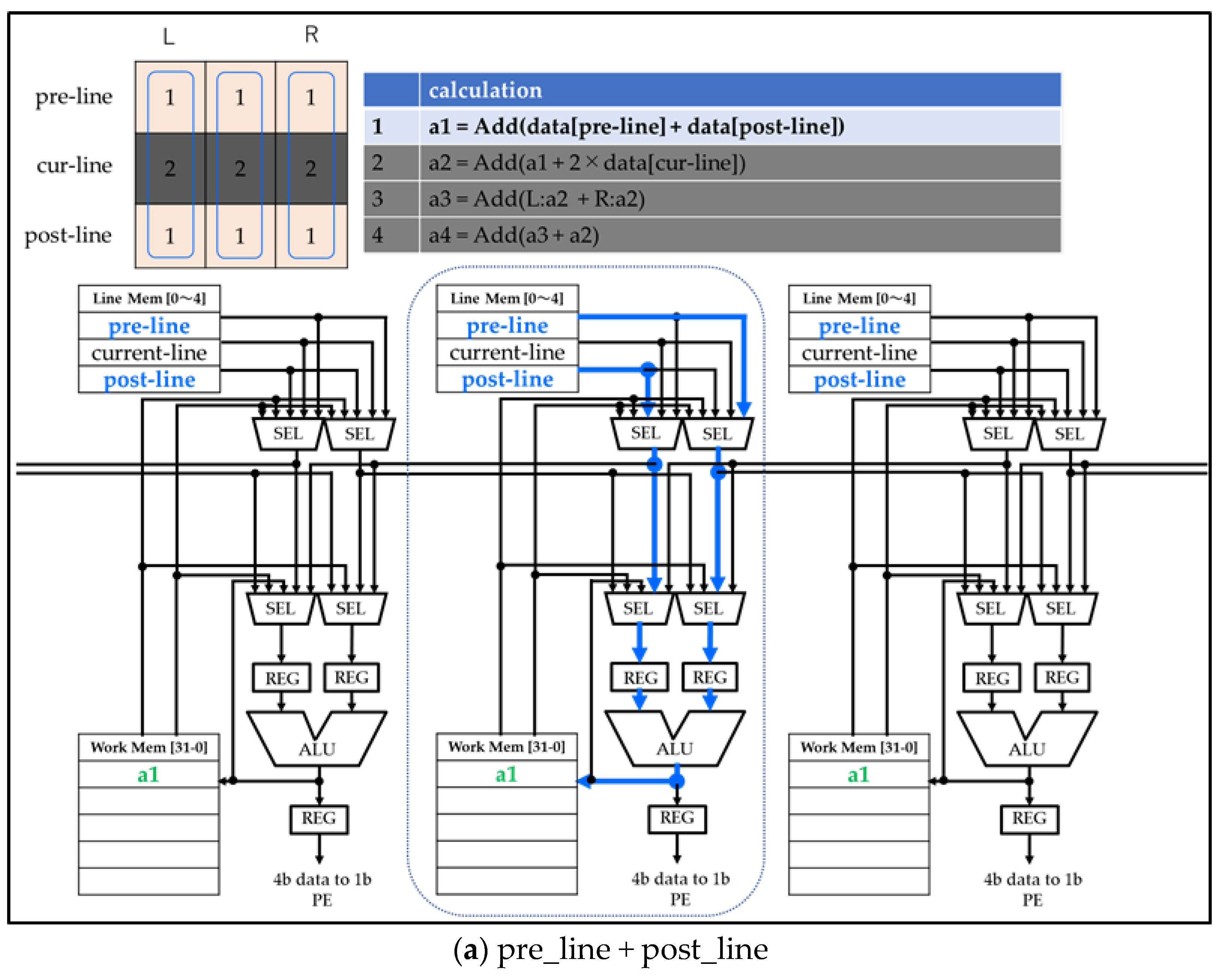
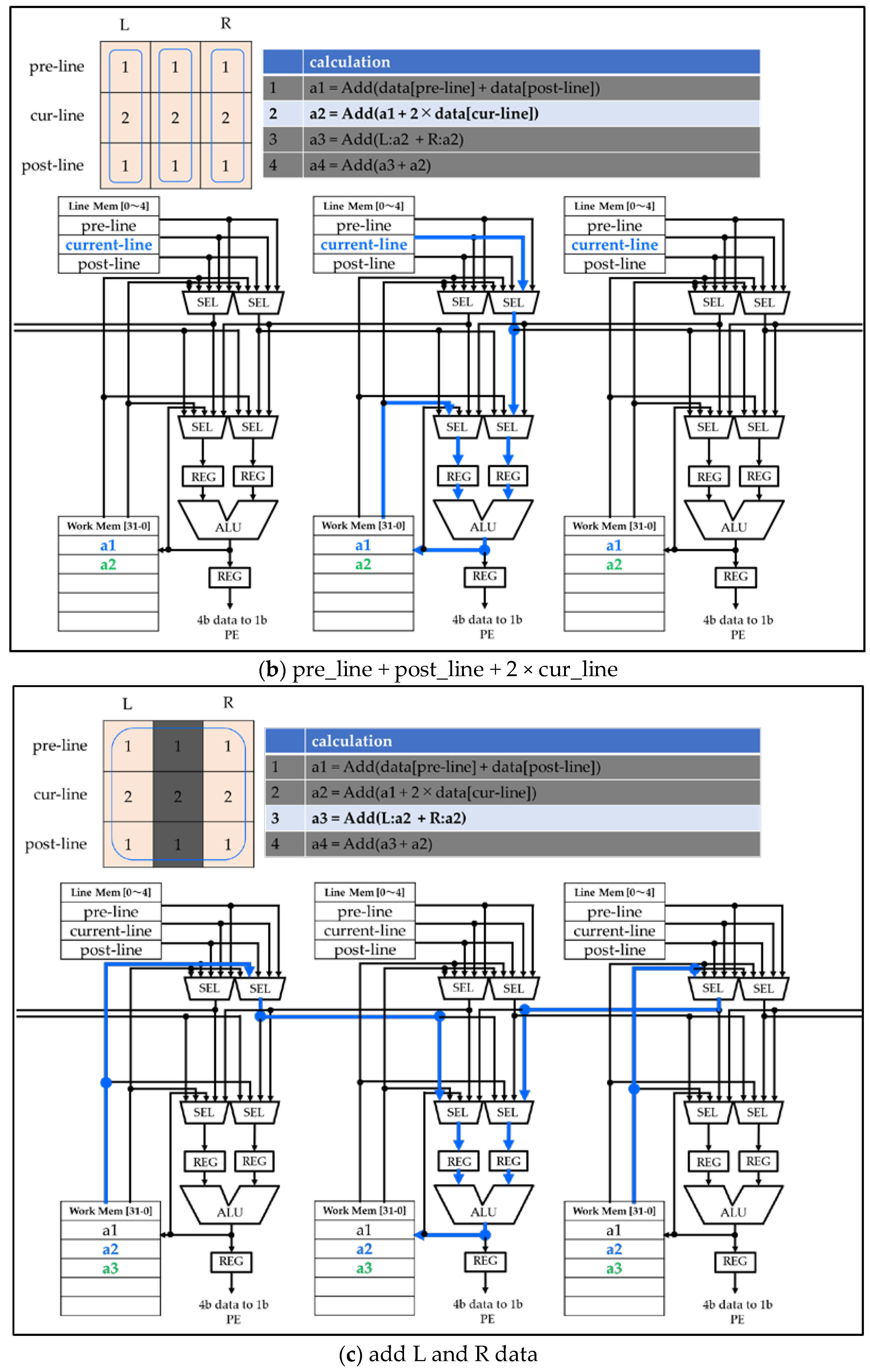
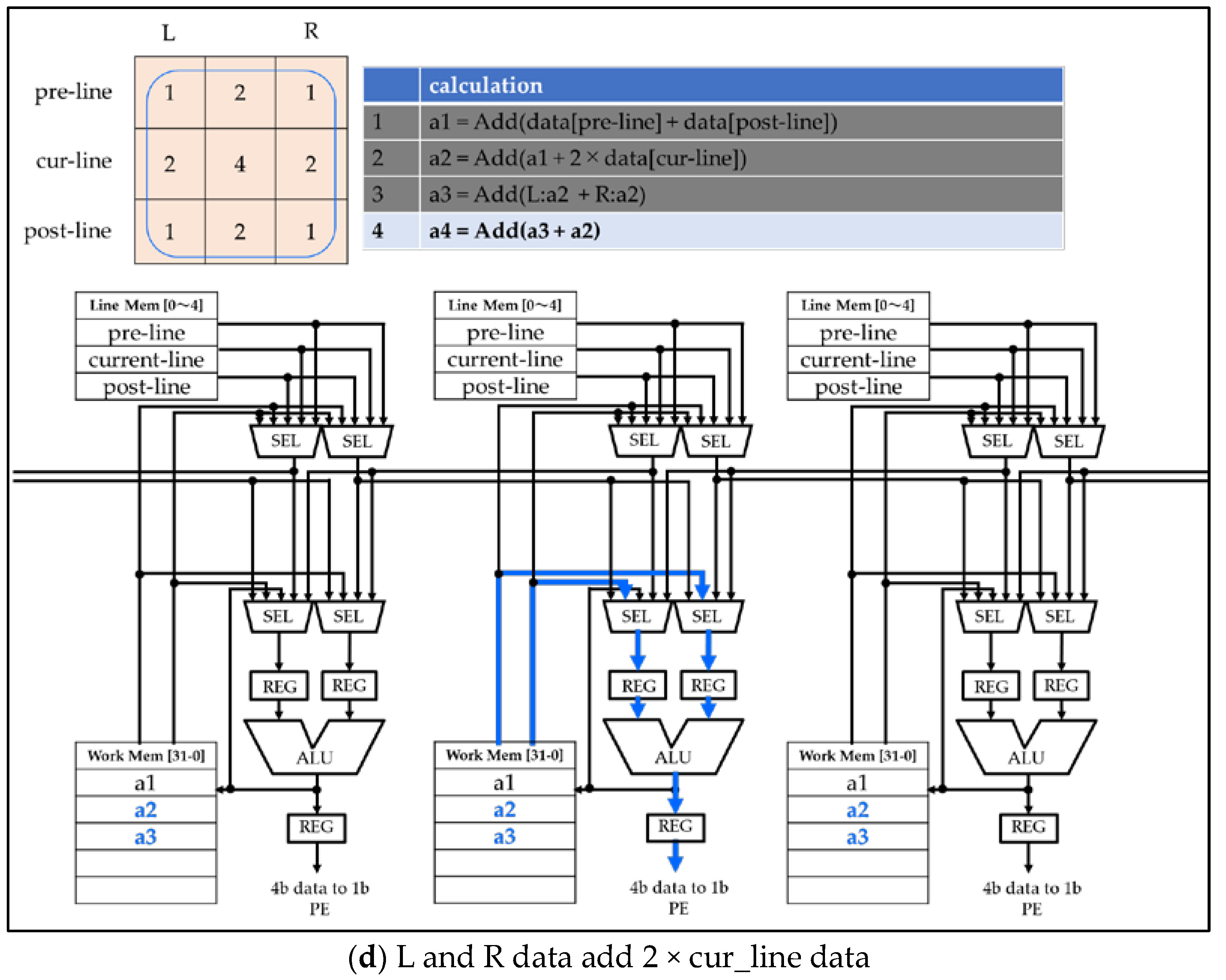
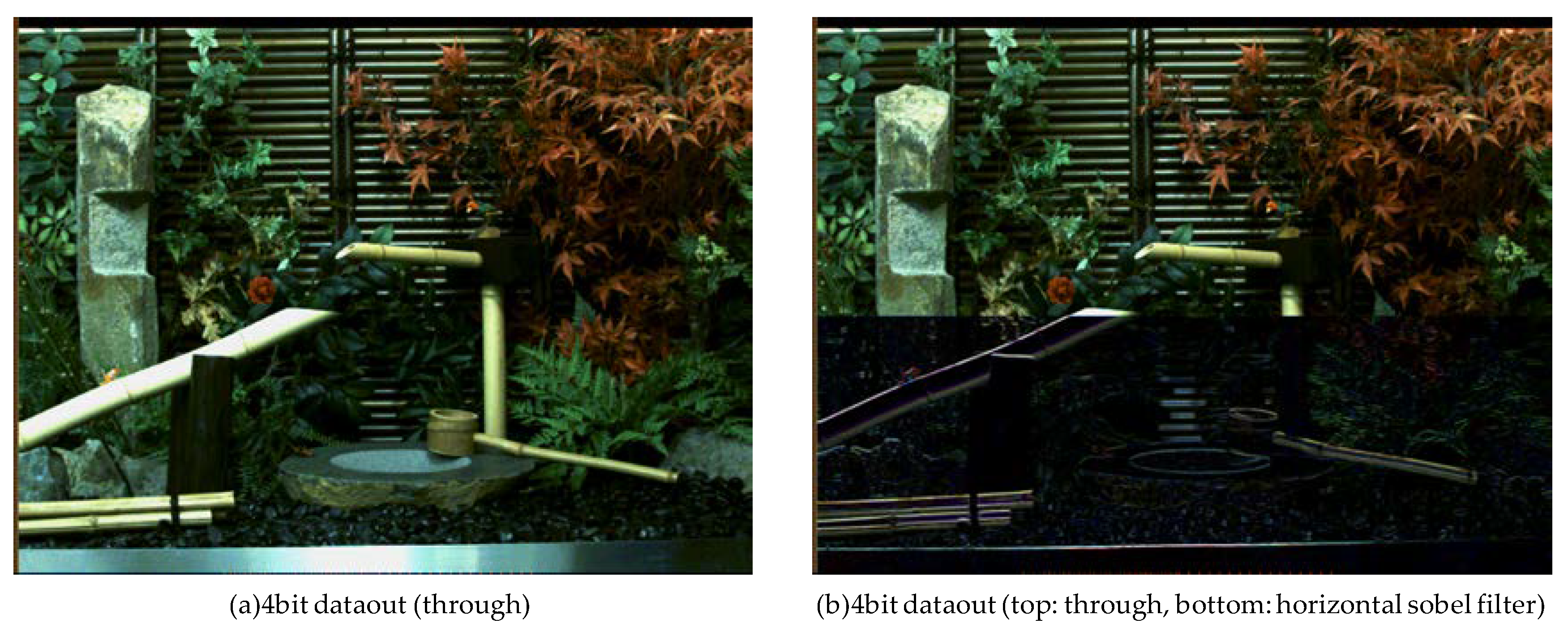
4.2. Programmable 4b Column Parallel PEs Spatial Processing Function
5. Applications
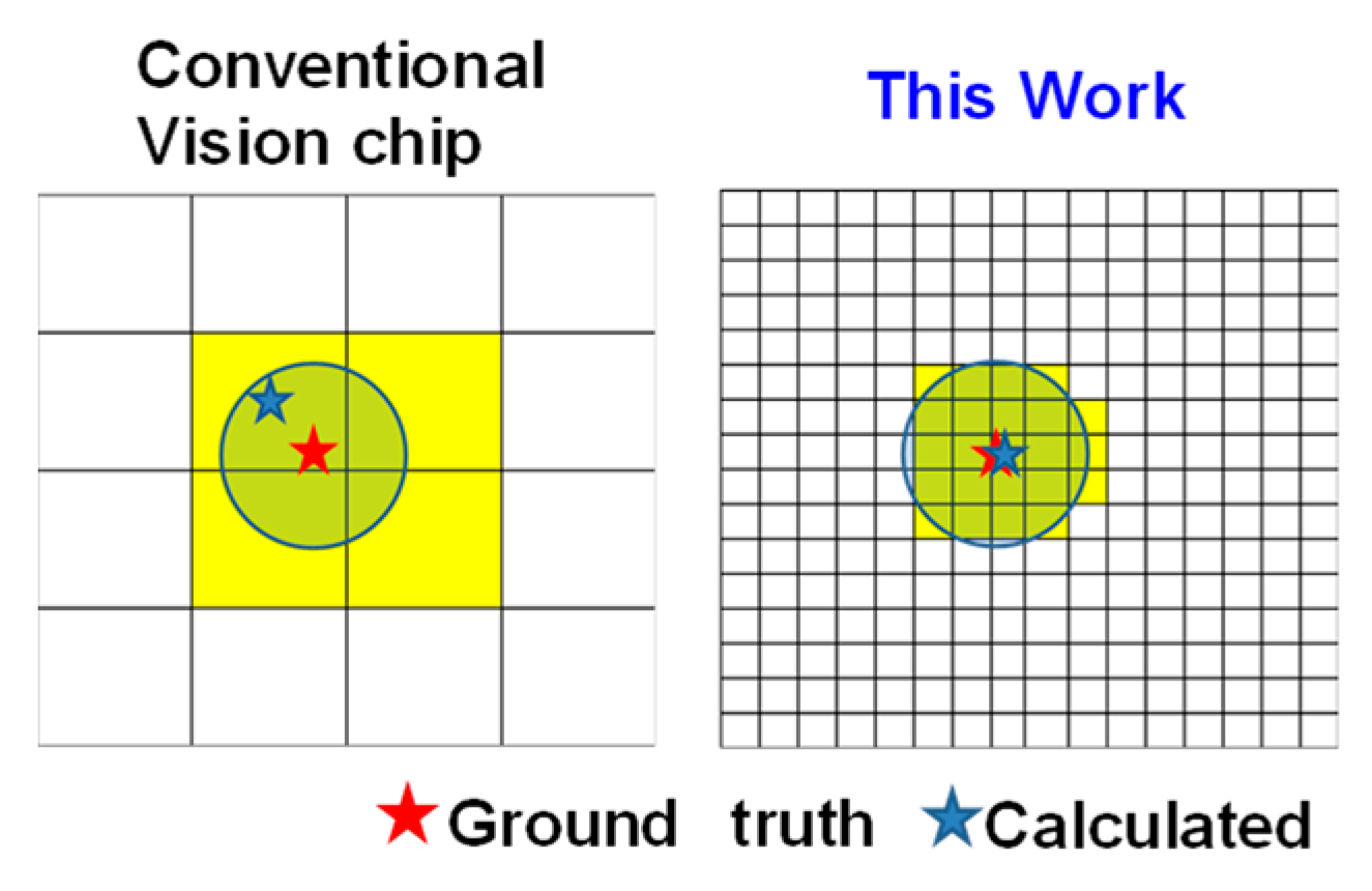
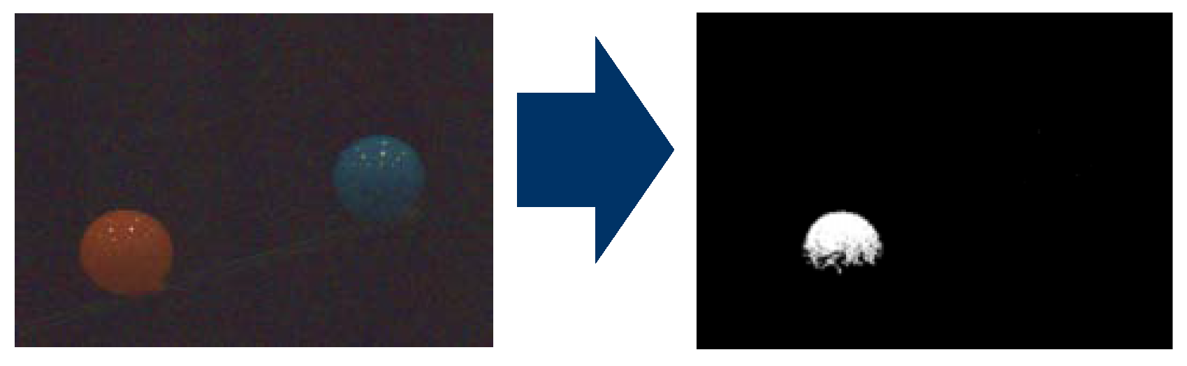
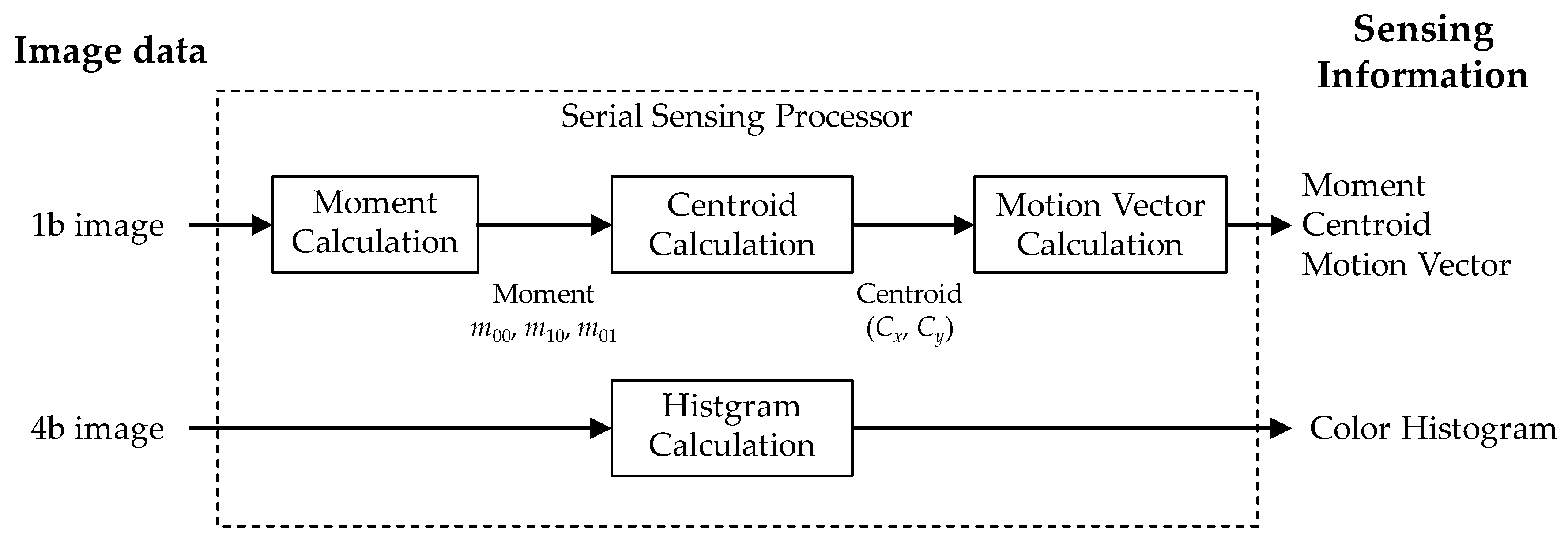
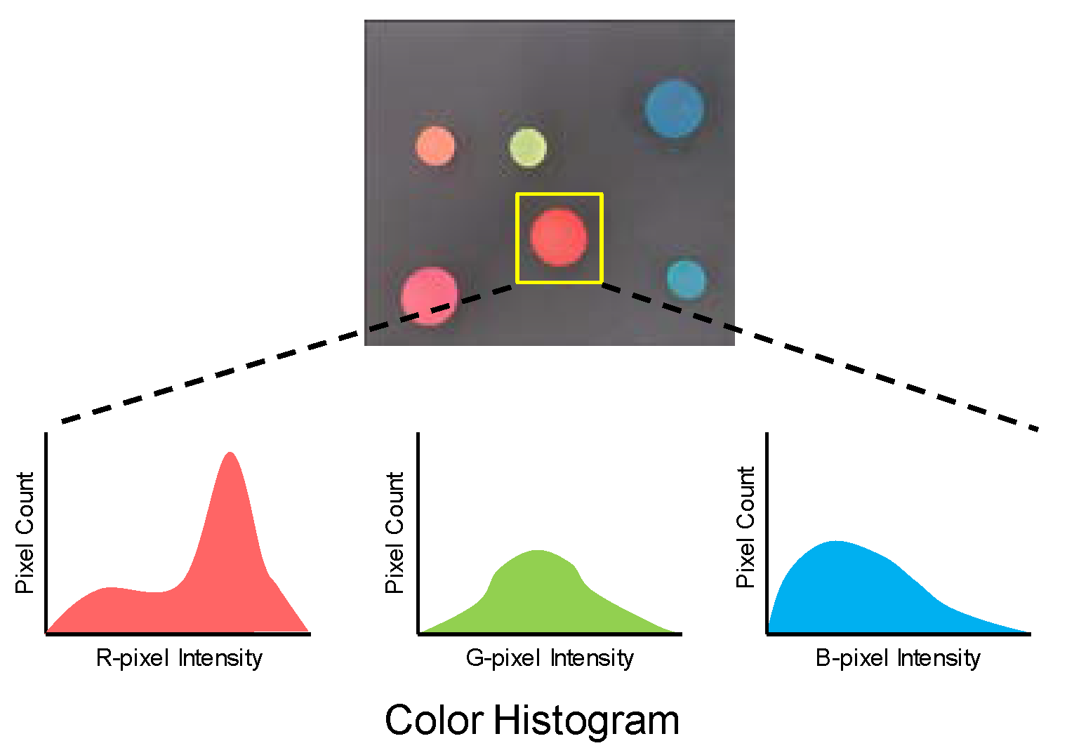
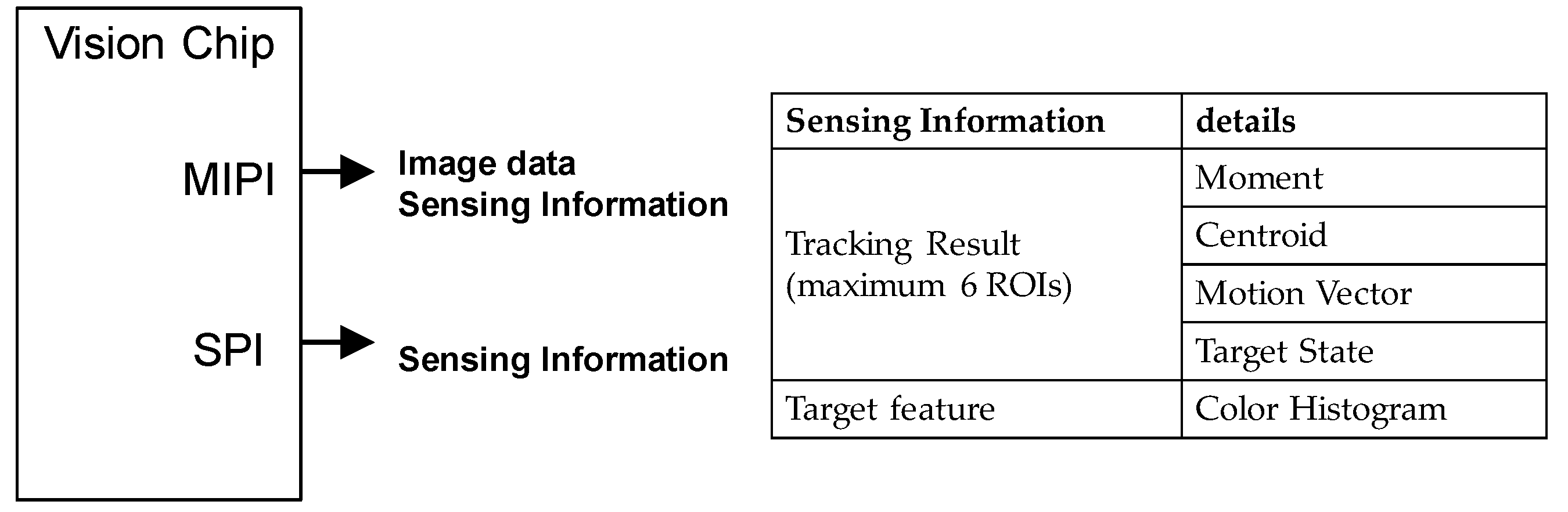
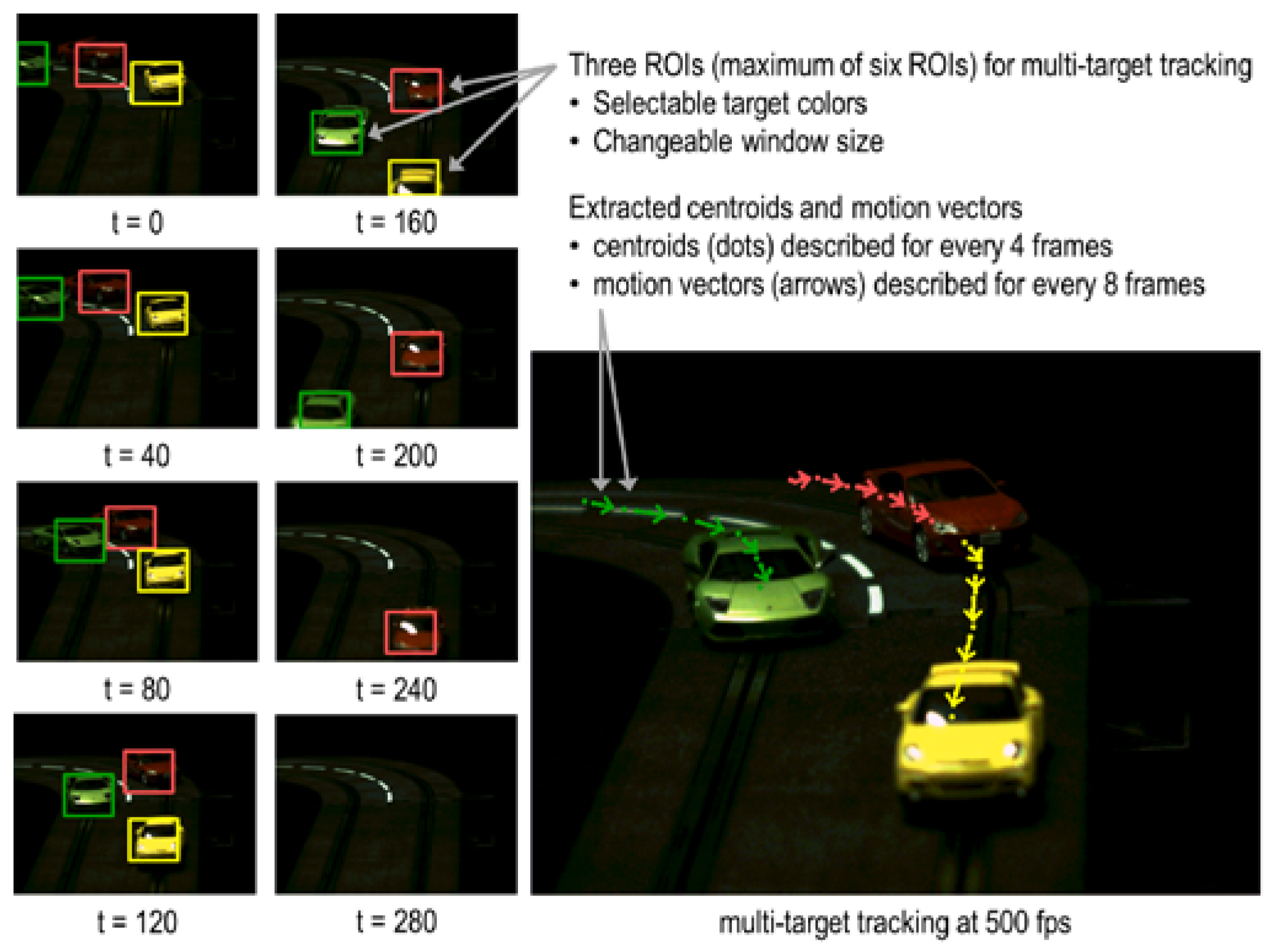
5.1. Multi-Target Tracking
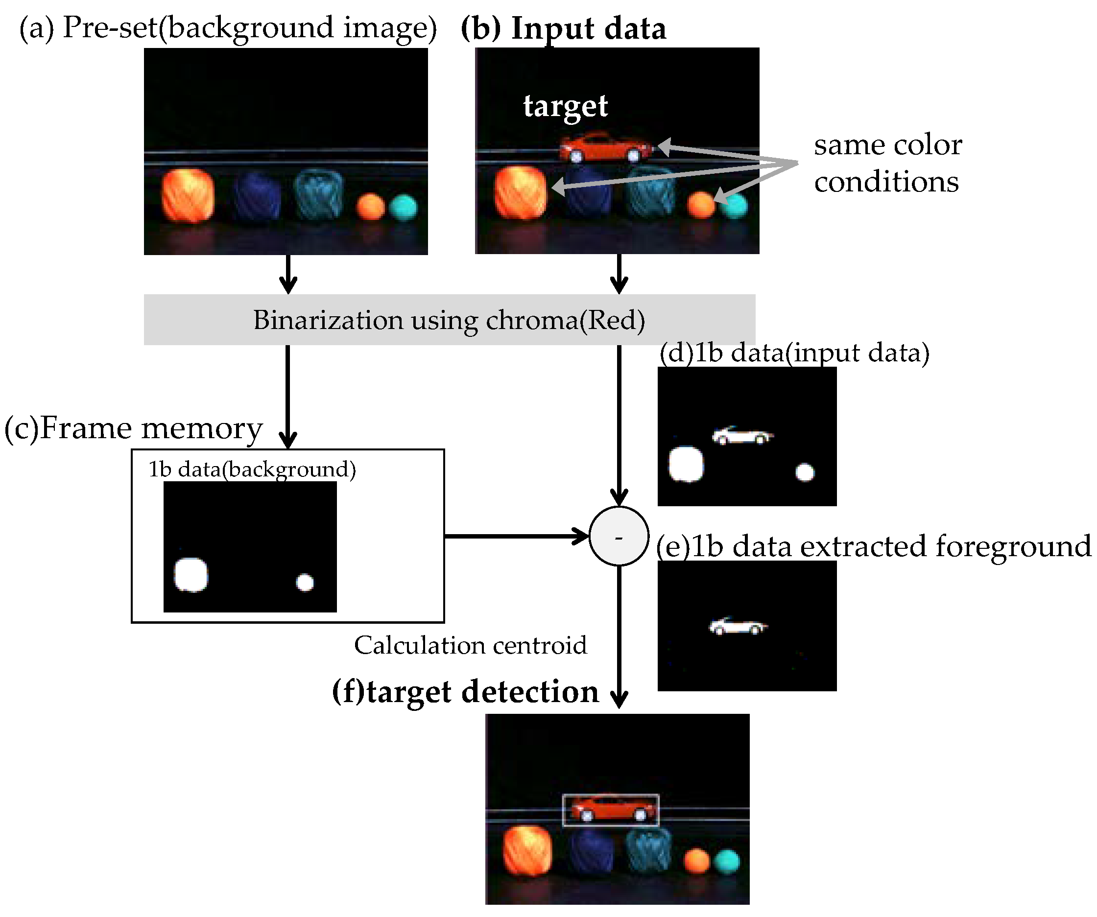
5.2. Foreground Extraction
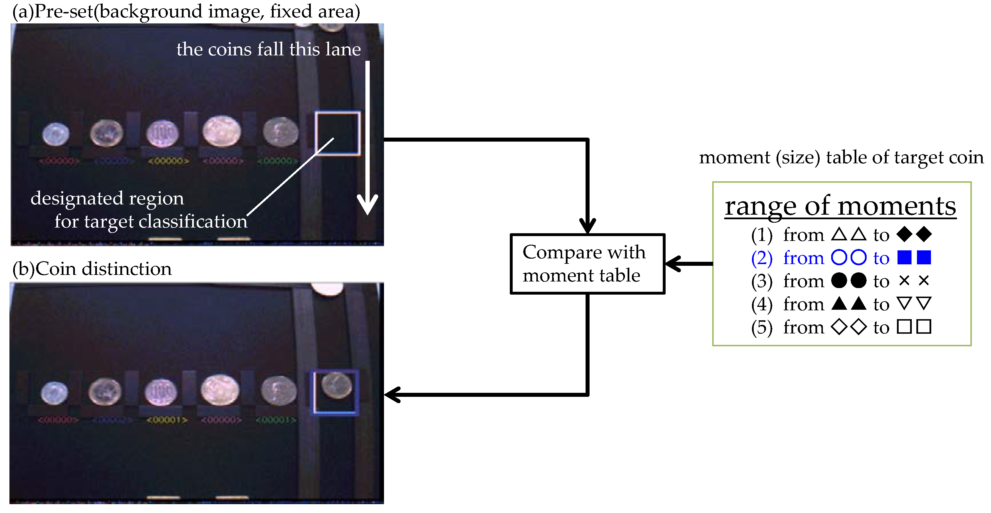
5.3. Multi-Target Classification
6. Conclusions
Author Contributions
Acknowledgments
Conflicts of Interest
References
- Ishikawa, M.; Ogawa, K.; Komuro, T.; Ishii, I. A CMOS vision chip with SIMD processing element array for 1ms image processing. In Proceedings of the 1999 IEEE International Solid-State Circuits Conference, Digest of Technical Papers, San Francisco, CA, USA, 17 February 1999; pp. 206–207. [Google Scholar]
- Shi, C.; Yang, J.; Han, Y.; Cao, Z.; Qin, Q.; Liu, L.; Wu, N.-J.; Wang, Z. A 1000 fps Vision Chip Based on Dynamically Reconfigurable Hybrid Architecture Comprising a PE Array and Self-Organizing Map Neural Network. IEEE J. Solid-State Circuits 2014, 49, 128–129. [Google Scholar] [CrossRef]
- Nakabo, Y.; Ishikawa, M.; Toyoda, H.; Mizuno, S. 1 ms Column Parallel Vision System and its Application of High Speed Target Tracking. In Proceedings of the IEEE International Conference on Robotics and Automation, San Francisco, CA, USA, 24–28 April 2000; Volume 1, pp. 650–655. [Google Scholar]
- Kawakami, H.; Igarashi, S.; Sasada, Y.; Akita, J. Column-Parallel Architecture for Line-of-Sight Detection Image Sensor Based on Centroid Calculation. ITE Trans. Media Technol. Appl. 2014, 2, 161–166. [Google Scholar] [CrossRef]
- Brandli, C.; Berner, R.; Yang, M.; Liu, S.-C.; Delbruck, T. A 240 × 180 130 dB 3 μs Latency Global Shutter Spatiotemporal Vision Sensor. IEEE J. Solid-State Circuits 2014, 49, 2333–2341. [Google Scholar] [CrossRef]
- Lichtsteiner, P.; Posch, C.; Delbruck, T. A 128 × 128 120 dB 15 μs Latency Asynchronous Temporal Contrast Vision Sensor. J. Solid-State Circuits 2007, 43, 566–576. [Google Scholar] [CrossRef]
- Posch, C.; Matolin, D.; Wohlgenannt, R. A QVGA 143 dB Dynamic Range Asynchronous Address-Event PWM Dynamic Image Sensor with Lossless Pixel-Level Video Compression. J. Solid-State Circuits 2011, 46, 259–275. [Google Scholar] [CrossRef]
- Son, B.; Suh, Y.; Kim, S.; Jung, H.; Kim, J.-S.; Shin, C.; Park, K.; Lee, K.; Park, J.; Woo, J.; et al. A 640 × 480 Dynamic Vision Sensor with a 9 μm Pixel and 300 Meps Address-Event Representation. In Proceedings of the 2017 IEEE International Solid-State Circuits Conference, San Francisco, CA, USA, 5–9 February 2017. [Google Scholar]
- Wakabayashi, H.; Yamaguchi, K.; Okano, M.; Nomoto, T. A 1/2.3-inch 10.3 Mpixel 50 frame/s Back-Illuminated CMOS Image Sensor. IEEE Int. Solid-State Circuits 2010, 53, 410–411. [Google Scholar]
- Toyama, T.; Mishina, K.; Tsuchiya, H.; Ichikawa, T.; Iwaki, H.; Gendai, Y.; Murakami, H.; Takamiya, K.; Shiroshita, H.; Muramatsu, Y.; et al. A 17.7 Mpixel 120 fps CMOS image sensor with 34.8 Gb/s readout. In Proceedings of the 2011 IEEE International Solid-State Circuits Conference, San Francisco, CA, USA, 20–24 February 2011; pp. 420–422. [Google Scholar]
- Sakakibara, M.; Oike, Y.; Takatsuka, T.; Kato, A.; Honda, K.; Taura, T.; Machida, T.; Okuno, J.; Ando, A.; Fukuro, T.; et al. An 83 dB-dynamic-range single-exposure global-shutter CMOS image sensor with in-pixel dual storage. In Proceedings of the 2012 IEEE International Solid-State Circuits Conference, San Francisco, CA, USA, 19–23 February 2012; pp. 380–381. [Google Scholar]
- Hirayama, T. The evolution of CMOS image sensors. In Proceedings of the 2013 IEEE Asian Solid-State Circuits Conference (A-SSCC), Singapore, 11–13 November 2013; pp. 5–8. [Google Scholar]
- Oike, Y.; Akiyama, K.; Hung, L.D.; Niitsuma, W.; Kato, A.; Sato, M.; Kato, Y.; Nakamura, W.; Shiroshita, H.; Sakano, Y.; et al. An 8.3 M-Pixel 480 fps global-shutter CMOS image sensor with gain-adaptive column ADCs and 2-on-1 stacked device structure. In Proceedings of the 2016 IEEE Symposium on VLSI Circuits (VLSI-Circuits), Honolulu, HI, USA, 15–17 June 2016; pp. 222–223. [Google Scholar]
- Sukegawa, S.; Umebayashi, T.; Nakajima, T.; Kawanobe, H.; Koseki, K.; Hirota, I.; Haruta, T.; Kasai, M.; Fukumoto, K.; Wakano, T.; et al. A 1/4-inch 8 Mpixel Back-Illuminated Stacked CMOS. In Proceedings of the 2013 IEEE International Solid-State Circuits Conference, Digest of Technical Papers, San Francisco, CA, USA, 17–21 February 2013; pp. 484–485. [Google Scholar]
- Yamazaki, T.; Katayama, H.; Uehara, S.; Nose, A.; Kobayashi, M.; Shida, S.; Odahara, M.; Takamiya, K.; Matsumoto, S.; Miyashita, L.; et al. A 1 ms High-Speed Vision Chip with 3D Stacked 140 GOPS Column Parallel PEs for Spatio-Temporal Image Processing. In Proceedings of the 2017 IEEE International Solid-State Circuits Conference (ISSCC), San Francisco, CA, USA, 5–9 February 2017. [Google Scholar]
- Kurokawa, M.; Hashiguchi, A.; Nakamura, K.; Okuda, H.; Aoyama, K.; Yamazaki, T.; Ohki, M.; Soneda, M.; Seno, K.; Kumata, I.; et al. 5.4 GOPS Linear Array Architecture DSP for Video−Format Conversion. In Proceedings of the 1996 IEEE International Solid-State Circuits Conference, San Francisco, CA, USA, 10 February 1996. [Google Scholar]
- Nakamura, K.; Kurokawa, M.; Hashiguchi, A.; Kanou, M.; Aoyama, K.; Okuda, H.; Iwase, S.; Yamazaki, T. Video DSP architecture and its application design methodology for sampling rate conversion. In Proceedings of the IEEE Workshop on VLSI Signal, San Francisco, CA, USA, 30 October–1 November 1996. [Google Scholar]
- Hashiguchi, A.; Kurokawa, M.; Nakamura, K.; Iwase, S. 5.4 GOPS, 81 GB/s Linear Array Architecture DSP. IEICE Trans. Electron. 1998, E81-C, 661–668. [Google Scholar]
- Yamazaki, T.; Nose, A.; Katayama, H.; Uehara, S.; Kobayashi, M.; Shida, S.; Odahara, M.; Takamiya, K.; Hisamatsu, Y.; Matsumoto, S.; et al. A 1 ms High-Speed Vision Chip with 3D Stacked 140 GOPS Column Parallel PEs for Diverse Sensing Applications. In Proceedings of the 2017 International Image Sensor Workshop, Hiroshima, Japan, 30 May–2 June 2017. [Google Scholar]
- Iwabuchi, S.; Maruyama, Y.; Ohgishi, Y.; Muramatsu, M.; Karasawa, N.; Hirayama, T. A Back-Illuminated High-Sensitivity Small-Pixel Color CMOS Image Sensor with Flexible Layout of Metal Wiring. In Proceedings of the 2006 IEEE International Solid State Circuits Conference, San Francisco, CA, USA, 6–9 February 2006; pp. 1171–1178. [Google Scholar]
- Ishii, I.; Ishikawa, M. Self-windowing for high speed vision. In Proceedings of the 1999 IEEE International Conference on Robotics and Automation (Cat. No.99CH36288C), Detroit, MI, USA, 10–15 May 1999; Volume 4, pp. 1916–1921. [Google Scholar]


| Function | Steps (for Column) |
|---|---|
| addition | length + 1 |
| subtraction | length + 1 |
| absolute value | length + 1 |
| comparison | length × 2 + 3 |
| select | length + 1 |
| maximum(minimum)value select | length × 2 + 2 |
| logical operation (and/or/xor/xnor/not) | length |
| swap | length + 3 |
| increment(decrement) | length + 1 |
| move | length |
| Functionality | Data in Frame Memory | |
|---|---|---|
| Self-Window [21] | Instructed target extraction | Dilated target image |
| Frame difference | Motion region extraction | Previous image |
| Background difference method | Foreground target extraction | Background image |
| Fabrication process | 90 nm 1P4M CIS/40 nm 1P7M Logic | |
| Supply voltage | 3.3 V/2.9 V/1.8 V/1.1 V | |
| Image size | Diagonal 5.678 mm (Type 1/3.2) | |
| Number of effective pixel | 1296 (H) × 976 (V) 1.27 Mpixels | |
| Pixel size | 3.50 µm (H) × 3.50 µm (V) | |
| Frame rate | Full | 60 fps at 1.27 Mpix 12b |
| 120 fps at 1.27 Mpix 10b | ||
| 500 fps at 1.27 Mpix 4b | ||
| 1/2 sub sampling | 120 fps at 0.31Mpix 12b | |
| 240 fps at 0.31Mpix 10b | ||
| 1000 fps at 0.31 Mpix 4b | ||
| Power consumption | 230 mW at 1.27 Mpixel 12b 60 fps | |
| 363 mW at 0.31 Mpixel 4b 1000 fps with sensing | ||
| (32 mW at only column PEs) | ||
| Saturation signal | 19,849 e− at 60 °C | |
| Sensitivity | 54,396 e−/lx·s | |
| (Green pixel, 3200 K light source with IR cut filter of 650 nm cut off) | ||
| RMS random noise | 2.1 e− (AnalogGain:30 dB) | |
| Dynamic range | 80 dB at 12b | |
| Maximum operating frequency | 108 MHz | |
| Processor count | 1 (CP) + 1304 (Column 4b/1bPE) | |
| Instruction cycle | 1 cycle | |
| Memory | Instruction memory 7 KByte | |
| Line memory 3 KByte | ||
| Frame memory 165 Kbyte | ||
| Template memory 12 KByte | ||
| Ref. No. | ISSCC 1999 [1] | ISSCC 2014 [2] | This Work |
|---|---|---|---|
| PE Structure |  |  |  |
| Resolution | 16 × 16 | 256 × 256 | 1304 × 968 |
| Pixel size | 150 μm × 150 μm | 10 μm × 10 μm | 3.5 μm × 3.5 μm |
| Pixel fill factor | 23% | 60% | 100% |
| Chip size | 100 mm2 | 82.3 mm2 | 25.7 mm2 |
| array efficiency | 0.45% | 3% | 50% |
| Maximum centroid error 1 | 6.25% | 0.39% | 0.08% |
| Power | N/A | 630 mW | 363 mW |
| Speed | N/A | 108 GOPS | 140 GOPS |
| Spatial Image Processing | Steps (for Column) | Time (108 MHz) |
|---|---|---|
| 4-neighbor-Gaussian | 21 | 190 ns |
| 8-neighbor-Gaussian | 26 | 241 ns |
| 4-neighbor-Laplacian | 42 | 389 ns |
| 4-neibor-Sharpness | 51 | 472 ns |
| 4-neighbor-Sobel | 79 | 732 ns |
© 2018 by the authors. Licensee MDPI, Basel, Switzerland. This article is an open access article distributed under the terms and conditions of the Creative Commons Attribution (CC BY) license (http://creativecommons.org/licenses/by/4.0/).
Share and Cite
Nose, A.; Yamazaki, T.; Katayama, H.; Uehara, S.; Kobayashi, M.; Shida, S.; Odahara, M.; Takamiya, K.; Matsumoto, S.; Miyashita, L.; et al. Design and Performance of a 1 ms High-Speed Vision Chip with 3D-Stacked 140 GOPS Column-Parallel PEs †. Sensors 2018, 18, 1313. https://doi.org/10.3390/s18051313
Nose A, Yamazaki T, Katayama H, Uehara S, Kobayashi M, Shida S, Odahara M, Takamiya K, Matsumoto S, Miyashita L, et al. Design and Performance of a 1 ms High-Speed Vision Chip with 3D-Stacked 140 GOPS Column-Parallel PEs †. Sensors. 2018; 18(5):1313. https://doi.org/10.3390/s18051313
Chicago/Turabian StyleNose, Atsushi, Tomohiro Yamazaki, Hironobu Katayama, Shuji Uehara, Masatsugu Kobayashi, Sayaka Shida, Masaki Odahara, Kenichi Takamiya, Shizunori Matsumoto, Leo Miyashita, and et al. 2018. "Design and Performance of a 1 ms High-Speed Vision Chip with 3D-Stacked 140 GOPS Column-Parallel PEs †" Sensors 18, no. 5: 1313. https://doi.org/10.3390/s18051313
APA StyleNose, A., Yamazaki, T., Katayama, H., Uehara, S., Kobayashi, M., Shida, S., Odahara, M., Takamiya, K., Matsumoto, S., Miyashita, L., Watanabe, Y., Izawa, T., Muramatsu, Y., Nitta, Y., & Ishikawa, M. (2018). Design and Performance of a 1 ms High-Speed Vision Chip with 3D-Stacked 140 GOPS Column-Parallel PEs †. Sensors, 18(5), 1313. https://doi.org/10.3390/s18051313