Low-Dimensional Materials and State-of-the-Art Architectures for Infrared Photodetection

Abstract
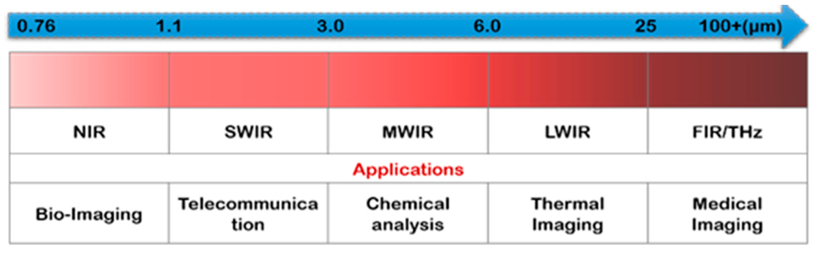
1. Introduction
2. Nanostructured IR Sensitive Materials for Photodetectors
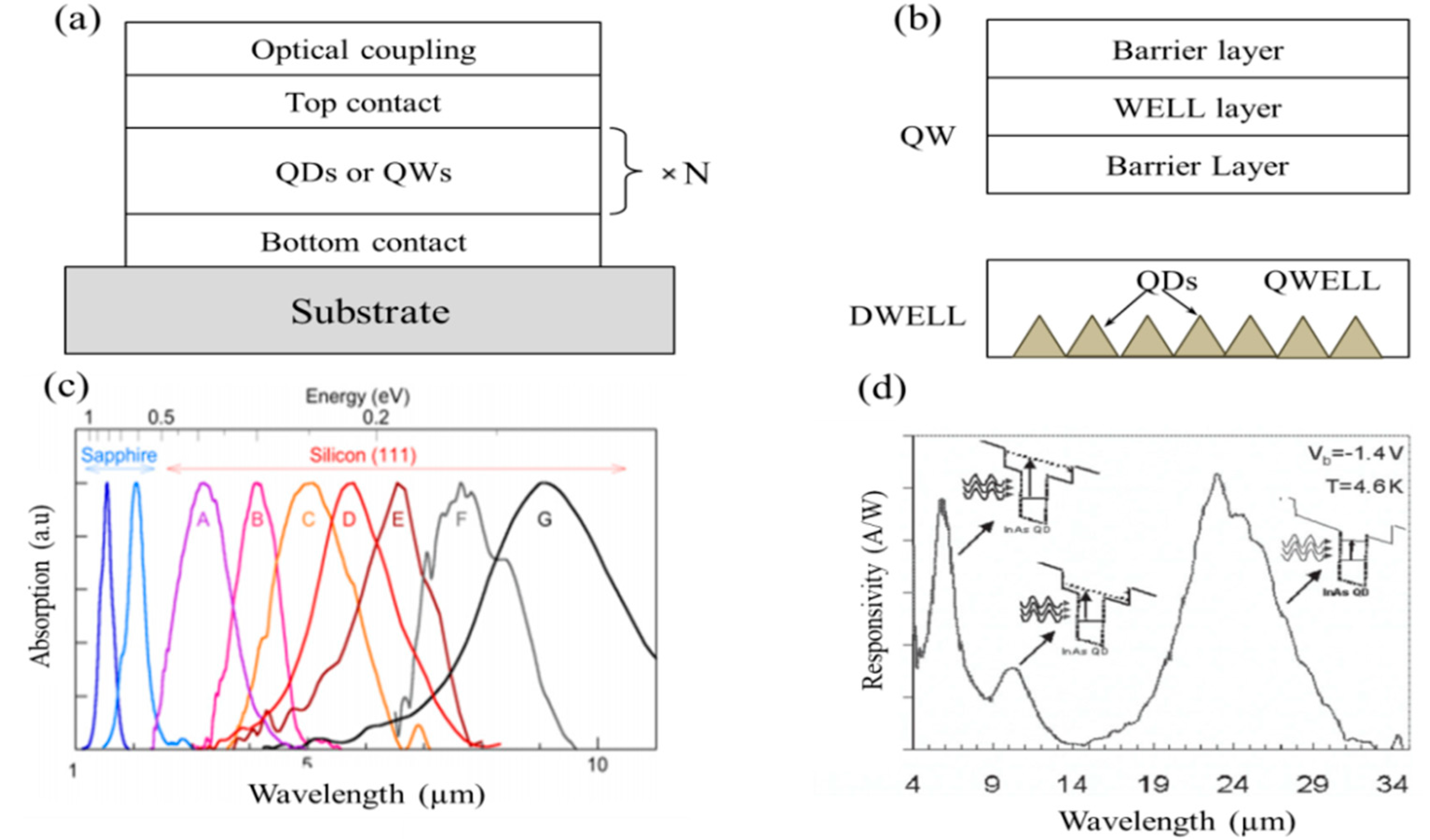
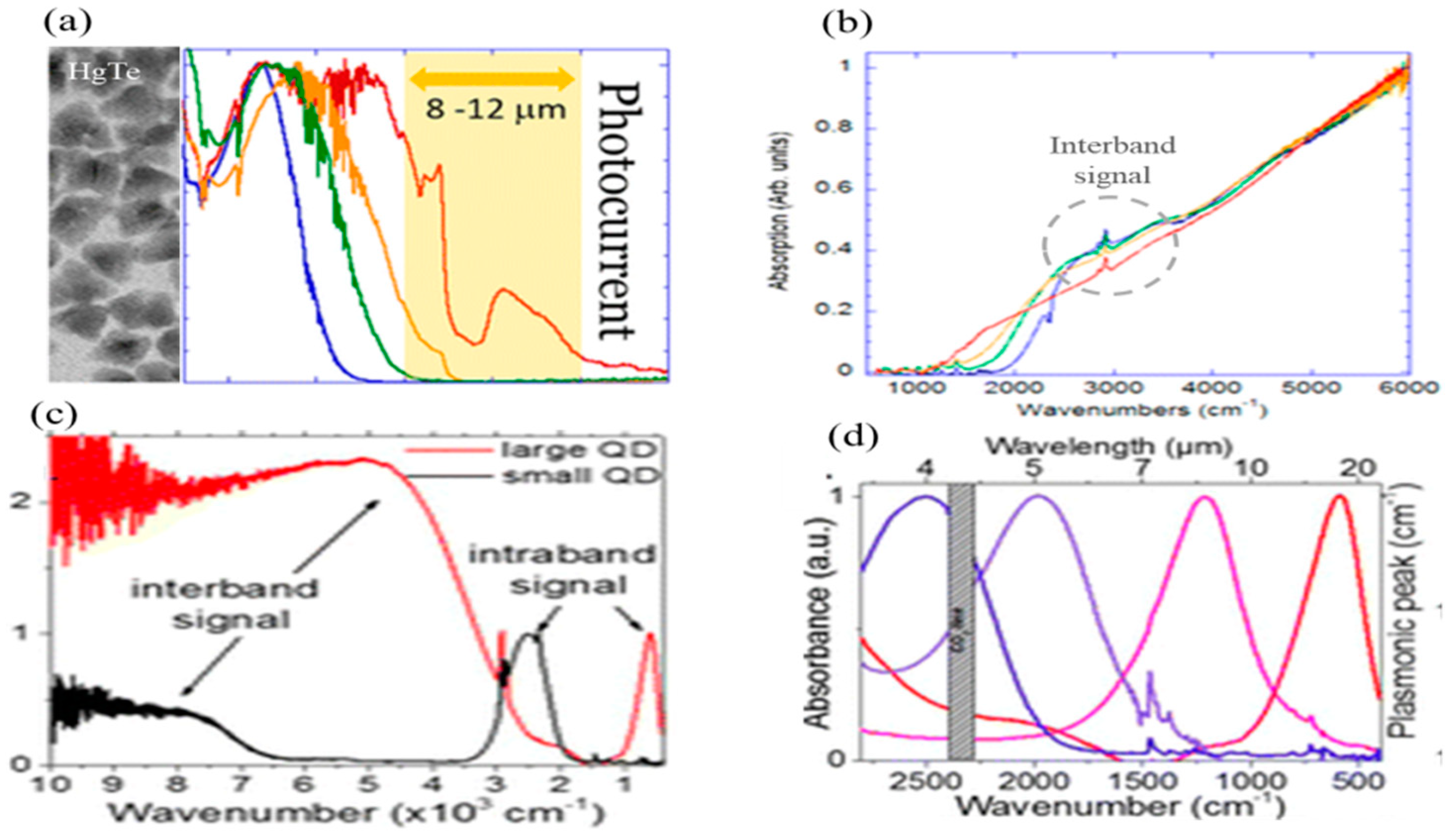
2.1. Quantum Dots and Quantum Wells-Based Photodetectors
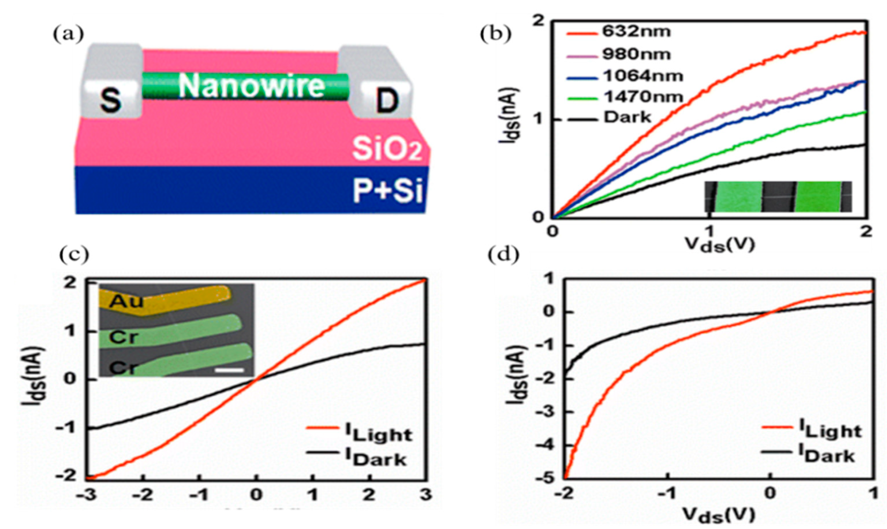
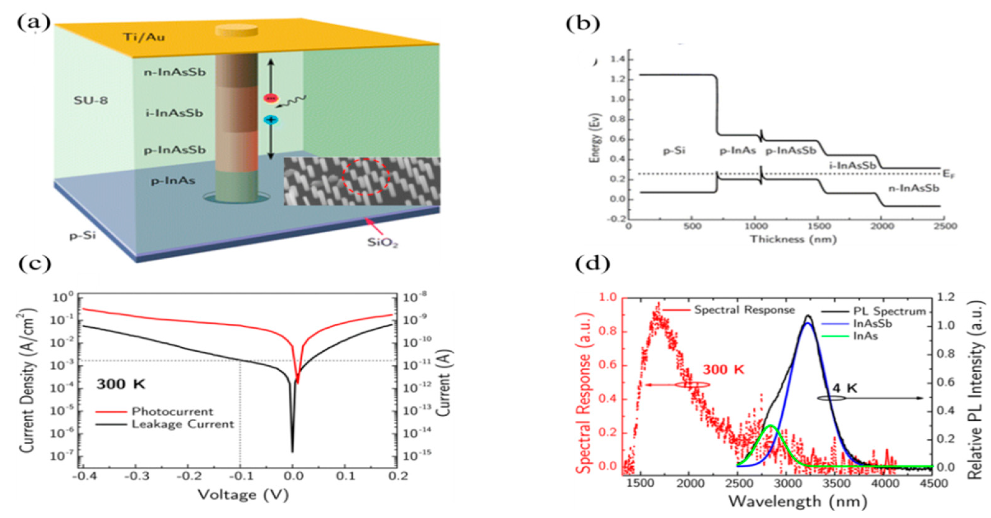
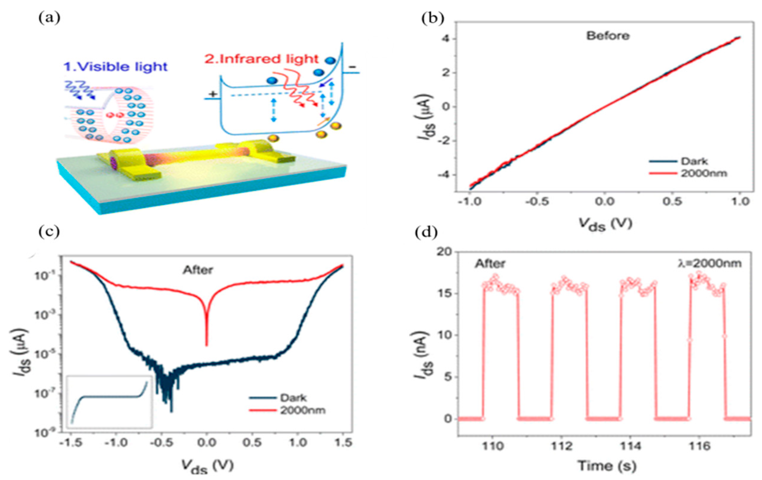
2.2. Nanowires
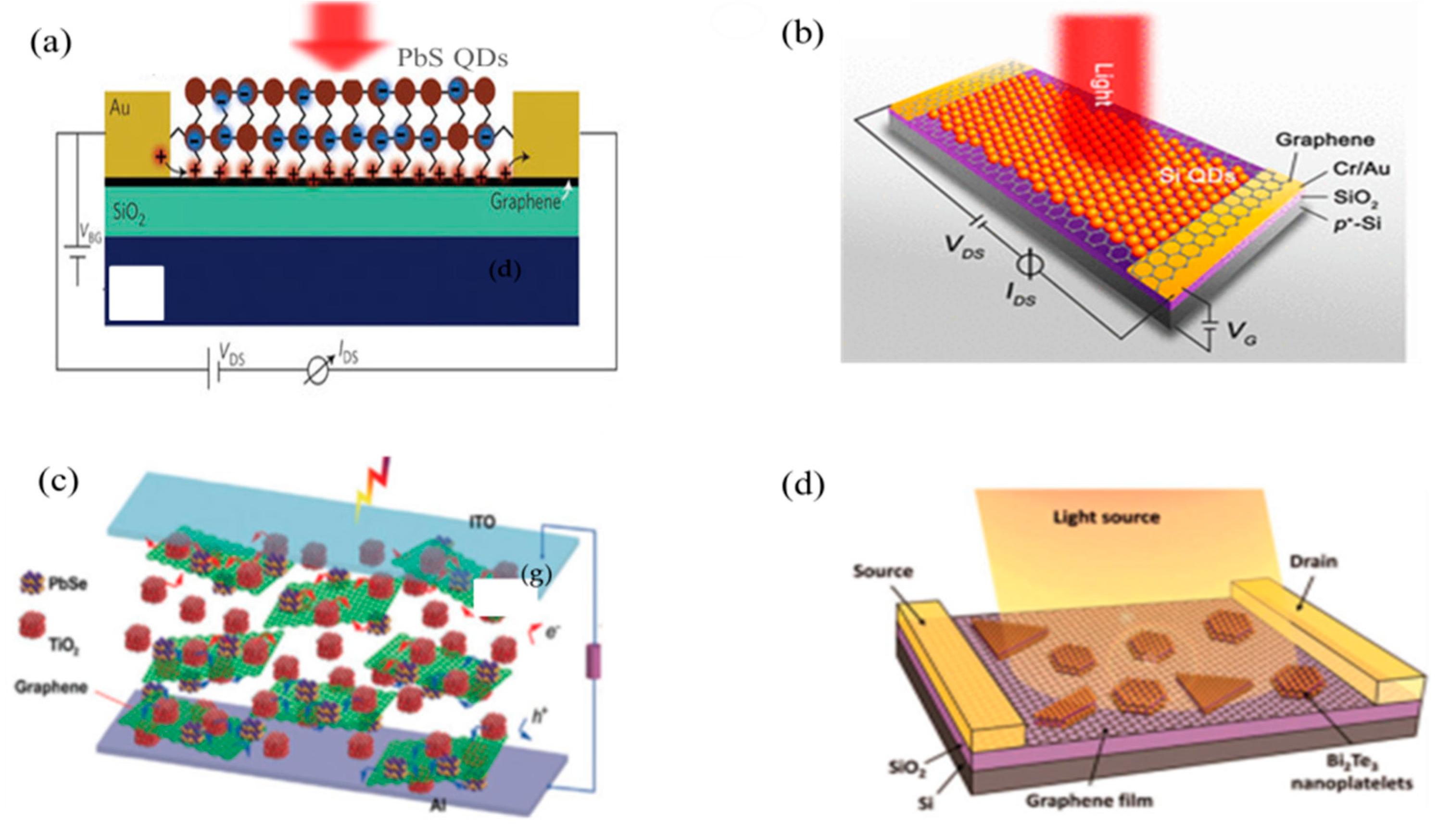
2.3. Black Phosphorus, Graphene, and Heterostructures
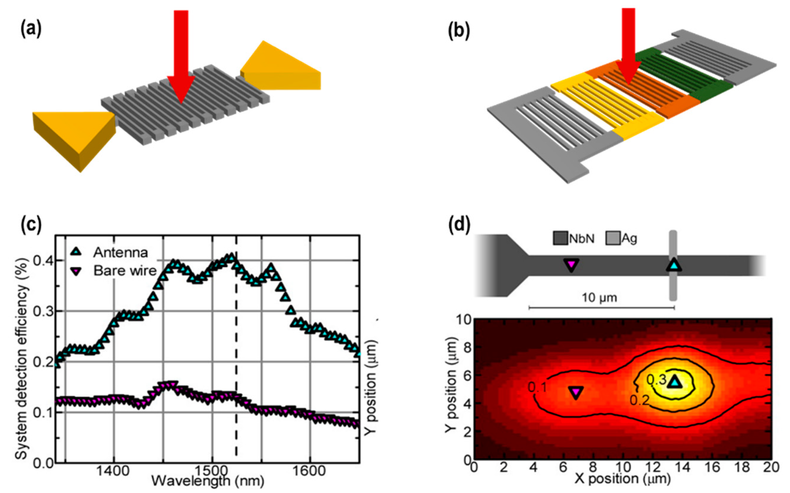
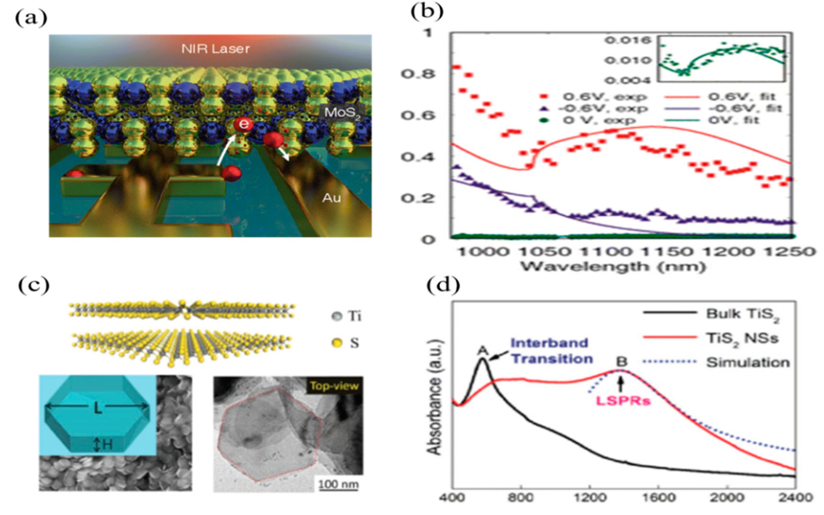
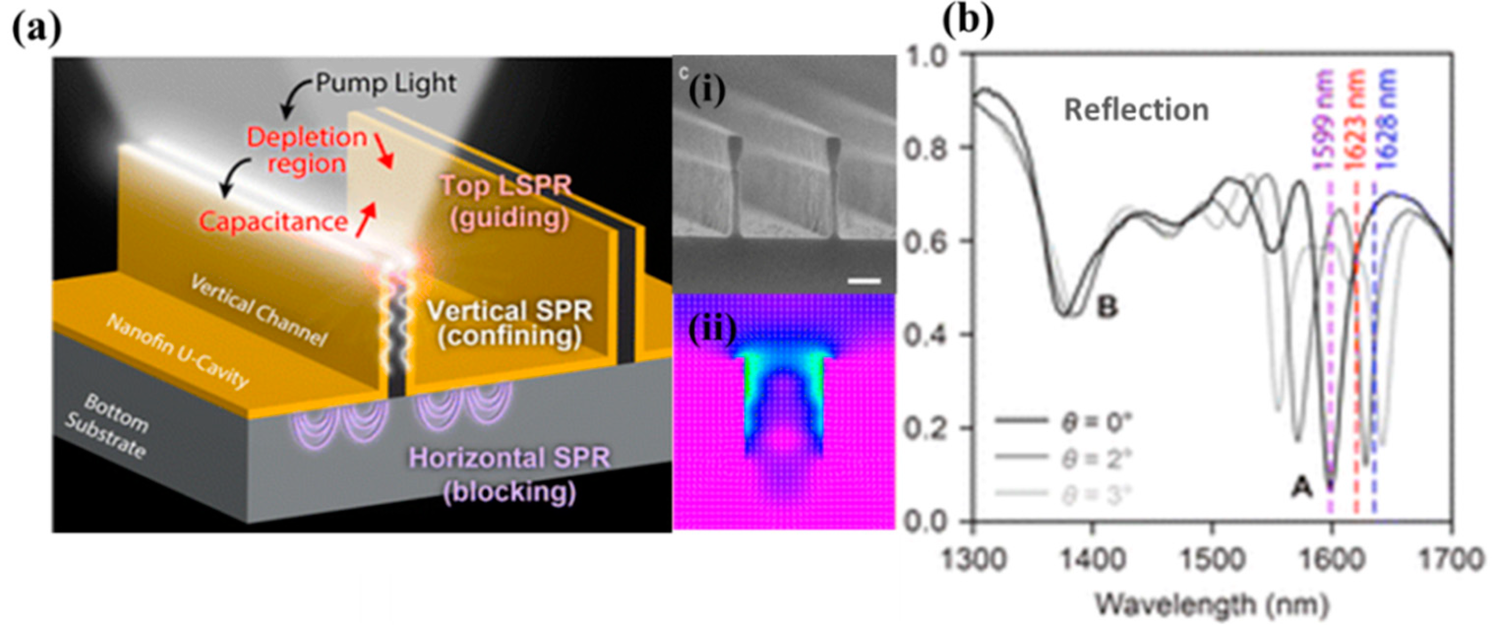
2.4. Plasmonic Nanostructures and Related Architectures
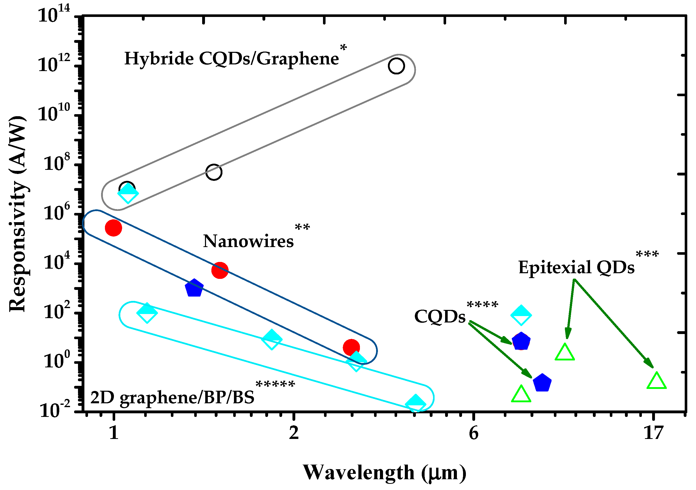
3. Summary
Funding
Acknowledgments
Conflicts of Interest
References
- Dawes, D.G.; Turner, D. Some Like It Hot|Features|Photonics Spectra. December 2008. Available online: https://www.photonics.com/Article.aspx?AID=35976 (accessed on 14 May 2018).
- Konstantatos, G.; Sargent, E.H. Nanostructured materials for photon detection. Nat. Nanotechnol. 2010, 5, 391–400. [Google Scholar] [CrossRef] [PubMed]
- Lefèvre, F.; Forget, F. Observed variations of methane on Mars unexplained by known atmospheric chemistry and physics. Nature 2009, 460, 720–723. [Google Scholar] [CrossRef] [PubMed]
- Saran, R.; Curry, R.J. Lead sulphide nanocrystal photodetector technologies. Nat. Photonics 2016, 10, 81–92. [Google Scholar] [CrossRef]
- Chitara, B.; Panchakarla, L.S.; Krupanidhi, S.B.; Rao, C.N.R. Infrared Photodetectors Based on Reduced Graphene Oxide and Graphene Nanoribbons. Adv. Mater. 2011, 23, 5419–5424. [Google Scholar] [CrossRef] [PubMed]
- Koppens, F.H.L.; Mueller, T.; Avouris, P.; Ferrari, A.C.; Vitiello, M.S.; Polini, M. Photodetectors based on graphene, other two-dimensional materials and hybrid systems. Nat. Nanotechnol. 2014, 9, 780–793. [Google Scholar] [CrossRef] [PubMed]
- Zhou, X.; Gan, L.; Zhang, Q.; Xiong, X.; Li, H.; Zhong, Z.; Han, J.; Zhai, T. High performance near-infrared photodetectors based on ultrathin SnS nanobelts grown via physical vapor deposition. J. Mater. Chem. C 2016, 4, 2111–2116. [Google Scholar] [CrossRef]
- Youngblood, N.; Chen, C.; Koester, S.J.; Li, M. Waveguide-integrated black phosphorus photodetector with high responsivity and low dark current. Nat. Photonics 2015, 9, 247–252. [Google Scholar] [CrossRef]
- Gao, J.; Nguyen, S.C.; Bronstein, N.D.; Alivisatos, A.P. Solution-Processed, High-Speed, and High-Quantum-Efficiency Quantum Dot Infrared Photodetectors. ACS Photonics 2016, 3, 1217–1222. [Google Scholar] [CrossRef]
- Konstantatos, G.; Badioli, M.; Gaudreau, L.; Osmond, J.; Bernechea, M.; de Arquer, F.P.G.; Gatti, F.; Koppens, F.H.L. Hybrid graphene–quantum dot phototransistors with ultrahigh gain. Nat. Nanotechnol. 2012, 7, 363–368. [Google Scholar] [CrossRef] [PubMed]
- Thompson, M.D.; Alhodaib, A.; Craig, A.P.; Robson, A.; Aziz, A.; Krier, A.; Svensson, J.; Wernersson, L.-E.; Sanchez, A.M.; Marshall, A.R.J. Low Leakage-Current InAsSb Nanowire Photodetectors on Silicon. Nano Lett. 2016, 16, 182–187. [Google Scholar] [CrossRef] [PubMed]
- Huh, J.; Yun, H.; Kim, D.-C.; Munshi, A.M.; Dheeraj, D.L.; Kauko, H.; van Helvoort, A.T.J.; Lee, S.; Fimland, B.-O.; Weman, H. Rectifying Single GaAsSb Nanowire Devices Based on Self-Induced Compositional Gradients. Nano Lett. 2015, 15, 3709–3715. [Google Scholar] [CrossRef] [PubMed]
- Lemme, M.C.; Koppens, F.H.L.; Falk, A.L.; Rudner, M.S.; Park, H.; Levitov, L.S.; Marcus, C.M. Gate-Activated Photoresponse in a Graphene p-n Junction. Nano Lett. 2011, 11, 4134–4137. [Google Scholar] [CrossRef] [PubMed]
- Kim, C.O.; Kim, S.; Shin, D.H.; Kang, S.S.; Kim, J.M.; Jang, C.W.; Joo, S.S.; Lee, J.S.; Kim, J.H.; Choi, S.-H.; et al. High photoresponsivity in an all-graphene p–n vertical junction photodetector. Nat. Commun. 2014, 5, 3249. [Google Scholar] [CrossRef] [PubMed]
- Nikitskiy, I.; Goossens, S.; Kufer, D.; Lasanta, T.; Navickaite, G.; Koppens, F.H.L.; Konstantatos, G. Integrating an electrically active colloidal quantum dot photodiode with a graphene phototransistor. Nat. Commun. 2016, 7, 11954. [Google Scholar] [CrossRef] [PubMed]
- Bandara, S.V.; Gunapala, S.D.; Liu, J.K.; Rafol, S.B.; Hill, C.J.; Ting, D.Z.-Y.; Mumolo, J.M.; Trinh, T.Q.; Fastenau, J.M.; Liu, A.W.K. Tuning and tailoring of broadband quantum-well infrared photodetector responsivity spectrum. Appl. Phys. Lett. 2005, 86, 151104. [Google Scholar] [CrossRef]
- Zhang, E.; Wang, P.; Li, Z.; Wang, H.; Song, C.; Huang, C.; Chen, Z.-G.; Yang, L.; Zhang, K.; Lu, S.; et al. Tunable Ambipolar Polarization-Sensitive Photodetectors Based on High-Anisotropy ReSe2 Nanosheets. ACS Nano 2016, 10, 8067–8077. [Google Scholar] [CrossRef] [PubMed]
- Singh, A.; Li, X.; Protasenko, V.; Galantai, G.; Kuno, M.; Xing, H.; Jena, D. Polarization-Sensitive Nanowire Photodetectors Based on Solution-Synthesized CdSe Quantum-Wire Solids. Nano Lett. 2007, 7, 2999–3006. [Google Scholar] [CrossRef] [PubMed]
- Yuan, H.; Liu, X.; Afshinmanesh, F.; Li, W.; Xu, G.; Sun, J.; Lian, B.; Curto, A.G.; Ye, G.; Hikita, Y.; et al. Polarization-sensitive broadband photodetector using a black phosphorus vertical p–n junction. Nat. Nanotechnol. 2015, 10, 707–713. [Google Scholar] [CrossRef] [PubMed]
- Lhuillier, E.; Scarafagio, M.; Hease, P.; Nadal, B.; Aubin, H.; Xu, X.Z.; Lequeux, N.; Patriarche, G.; Ithurria, S.; Dubertret, B. Infrared Photodetection Based on Colloidal Quantum-Dot Films with High Mobility and Optical Absorption up to THz. Nano Lett. 2016, 16, 1282–1286. [Google Scholar] [CrossRef] [PubMed]
- Lee, S.J.; Ku, Z.; Barve, A.; Montoya, J.; Jang, W.-Y.; Brueck, S.R.J.; Sundaram, M.; Reisinger, A.; Krishna, S.; Noh, S.K. A monolithically integrated plasmonic infrared quantum dot camera. Nat. Commun. 2011, 2, 286. [Google Scholar] [CrossRef] [PubMed]
- Wu, W.; Bonakdar, A.; Mohseni, H. Plasmonic enhanced quantum well infrared photodetector with high detectivity. Appl. Phys. Lett. 2010, 96, 161107. [Google Scholar] [CrossRef]
- Shishodia, M.S.; Unil Perera, A.G. Heterojunction plasmonic midinfrared detectors. J. Appl. Phys. 2011, 109, 043108. [Google Scholar] [CrossRef]
- Shenoi, R.V.; Rosenberg, J.; Vandervelde, T.E.; Painter, O.J.; Krishna, S. Multispectral Quantum Dots-in-a-Well Infrared Detectors Using Plasmon Assisted Cavities. IEEE J. Quantum Electron. 2010, 46, 1051–1057. [Google Scholar] [CrossRef]
- Fang, Z.; Liu, Z.; Wang, Y.; Ajayan, P.M.; Nordlander, P.; Halas, N.J. Graphene-Antenna Sandwich Photodetector. Nano Lett. 2012, 12, 3808–3813. [Google Scholar] [CrossRef] [PubMed]
- Crouch, C.H.; Carey, J.E.; Shen, M.; Mazur, E.; Genin, F.Y. Infrared absorption by sulfur-doped silicon formed by femtosecond laser irradiation. Appl. Phys. A 2004, 79, 1635–1641. [Google Scholar] [CrossRef]
- Zhong, H.; Guo, A.; Guo, G.; Li, W.; Jiang, Y. The Enhanced Light Absorptance and Device Application of Nanostructured Black Silicon Fabricated by Metal-assisted Chemical Etching. Nanoscale Res. Lett. 2016, 11, 322. [Google Scholar] [CrossRef] [PubMed]
- Ariyawansa, G.; Perera, A.G.U.; Su, X.H.; Chakrabarti, S.; Bhattacharya, P. Multi-color tunneling quantum dot infrared photodetectors operating at room temperature. Infrared Phys. Technol. 2007, 50, 156–161. [Google Scholar] [CrossRef]
- Tian, Z.-B.; Schuler-Sandy, T.; Krishna, S. Electron barrier study of mid-wave infrared interband cascade photodetectors. Appl. Phys. Lett. 2013, 103, 083501. [Google Scholar] [CrossRef]
- Gendron, L.; Koeniguer, C.; Berger, V.; Marcadet, X. High resistance narrow band quantum cascade photodetectors. Appl. Phys. Lett. 2005, 86, 121116. [Google Scholar] [CrossRef]
- Chakrabarti, S.; Adhikary, S.; Halder, N.; Aytac, Y.; Perera, A.G.U. High-performance, long-wave (∼10.2 μ m) InGaAs/GaAs quantum dot infrared photodetector with quaternary In 0.21 Al 0.21 Ga 0.58 As capping. Appl. Phys. Lett. 2011, 99, 181102. [Google Scholar] [CrossRef]
- Goubet, N.; Jagtap, A.; Livache, C.; Martinez, B.; Portalès, H.; Xu, X.Z.; Lobo, R.P.S.M.; Dubertret, B.; Lhuillier, E. Terahertz HgTe Nanocrystals: Beyond Confinement. J. Am. Chem. Soc. 2018, 140, 5033–5036. [Google Scholar] [CrossRef] [PubMed]
- Chen, M.; Lu, H.; Abdelazim, N.M.; Zhu, Y.; Wang, Z.; Ren, W.; Kershaw, S.V.; Rogach, A.L.; Zhao, N. Mercury Telluride Quantum Dot Based Phototransistor Enabling High-Sensitivity Room-Temperature Photodetection at 2000 nm. ACS Nano 2017, 11, 5614–5622. [Google Scholar] [CrossRef] [PubMed]
- Tang, X.; Wu, G.F.; Lai, K.W.C. Plasmon resonance enhanced colloidal HgSe quantum dot filterless narrowband photodetectors for mid-wave infrared. J. Mater. Chem. C. 2017, 5, 362–369. [Google Scholar] [CrossRef]
- Konstantatos, G.; Howard, I.; Fischer, A.; Hoogland, S.; Clifford, J.; Klem, E.; Levina, L.; Sargent, E.H. Ultrasensitive solution-cast quantum dot photodetectors. Nature 2006, 442, 180–183. [Google Scholar] [CrossRef] [PubMed]
- Zheng, D.; Wang, J.; Hu, W.; Liao, L.; Fang, H.; Guo, N.; Wang, P.; Gong, F.; Wang, X.; Fan, Z.; et al. When Nanowires Meet Ultrahigh Ferroelectric Field–High-Performance Full-Depleted Nanowire Photodetectors. Nano Lett. 2016, 16, 2548–2555. [Google Scholar] [CrossRef] [PubMed]
- Miao, J.; Hu, W.; Guo, N.; Lu, Z.; Zou, X.; Liao, L.; Shi, S.; Chen, P.; Fan, Z.; Ho, J.C.; et al. Single InAs Nanowire Room-Temperature Near-Infrared Photodetectors. ACS Nano 2014, 8, 3628–3635. [Google Scholar] [CrossRef] [PubMed]
- Fang, H.; Hu, W.; Wang, P.; Guo, N.; Luo, W.; Zheng, D.; Gong, F.; Luo, M.; Tian, H.; Zhang, X.; et al. Visible Light-Assisted High-Performance Mid-Infrared Photodetectors Based on Single InAs Nanowire. Nano Lett. 2016, 16, 6416–6424. [Google Scholar] [CrossRef] [PubMed]
- Sun, Z.; Liu, Z.; Li, J.; Tai, G.; Lau, S.-P.; Yan, F. Infrared Photodetectors Based on CVD-Grown Graphene and PbS Quantum Dots with Ultrahigh Responsivity. Adv. Mater. 2012, 24, 5878–5883. [Google Scholar] [CrossRef] [PubMed]
- Ni, Z.; Ma, L.; Du, S.; Xu, Y.; Yuan, M.; Fang, H.; Wang, Z.; Xu, M.; Li, D.; Yang, J.; et al. Plasmonic Silicon Quantum Dots Enabled High-Sensitivity Ultrabroadband Photodetection of Graphene-Based Hybrid Phototransistors. ACS Nano 2017, 11, 9854–9862. [Google Scholar] [CrossRef] [PubMed]
- Cao, F.; Liao, Q.; Deng, K.; Chen, L.; Li, L.; Zhang, Y. Novel perovskite/TiO2/Si trilayer heterojunctions for high-performance self-powered ultraviolet-visible-near infrared (UV-Vis-NIR) photodetectors. Nano Res. 2018, 11, 1722–1730. [Google Scholar] [CrossRef]
- Tsao, S.; Lim, H.; Seo, H.; Zhang, W.; Razeghi, M. InP-Based Quantum-Dot Infrared Photodetectors With High Quantum Efficiency and High-Temperature Imaging. IEEE Sens. J. 2008, 8, 936–941. [Google Scholar] [CrossRef]
- Durmaz, H.; Sookchoo, P.; Cui, X.; Jacobson, R.; Savage, D.E.; Lagally, M.G.; Paiella, R. SiGe Nanomembrane Quantum-Well Infrared Photodetectors. ACS Photonics 2016, 3, 1978–1985. [Google Scholar] [CrossRef]
- Rogalski, A. Infrared detectors: Status and trends. Prog. Quantum Electron. 2003, 27, 59–210. [Google Scholar] [CrossRef]
- Pan, J.L.; Fonstad, C.G. Theory, fabrication and characterization of quantum well infrared photodetectors. Mater. Sci. Eng. 2000, 28, 65–147. [Google Scholar] [CrossRef]
- Sakata, H. Optimally designed layer formation for wavelength-selective photodetectors based on grating-assisted coupling. Opt. Quantum Electron. 1996, 28, 1129–1138. [Google Scholar] [CrossRef]
- Le, D.T.; Morath, C.P.; Norton, H.E.; Cardimona, D.A.; Raghavan, S.; Rotella, P.; Stintz, S.A.; Fuchs, B.; Krishna, S. High responsivity, LWIR dots-in-a-well quantum dot infrared photodetectors. Infrared Phys. Technol. 2003, 44, 517–526. [Google Scholar] [CrossRef]
- Wang, X.-J.; Zhai, S.-Q.; Zhuo, N.; Liu, J.-Q.; Liu, F.-Q.; Liu, S.-M.; Wang, Z.-G. Quantum dot quantum cascade infrared photodetector. Appl. Phys. Lett. 2014, 104, 171108. [Google Scholar] [CrossRef]
- Machhadani, H.; Kandaswamy, P.; Sakr, S.; Vardi, A.; Wirtmüller, A.; Nevou, L.; Guillot, F.; Pozzovivo, G.; Tchernycheva, M.; Lupu, A.; et al. GaN/AlGaN intersubband optoelectronic devices. New J. Phys. 2009, 11, 125023. [Google Scholar] [CrossRef]
- Krishna, S.; Gunapala, S.D.; Bandara, S.V.; Hill, C.; Ting, D.Z. Quantum Dot Based Infrared Focal Plane Arrays. Proc. IEEE 2007, 95, 1838–1852. [Google Scholar] [CrossRef]
- Nevou, L.; Liverini, V.; Castellano, F.; Bismuto, A.; Faist, J. Asymmetric heterostructure for photovoltaic InAs quantum dot infrared photodetector. Appl. Phys. Lett. 2010, 97, 023505. [Google Scholar] [CrossRef]
- Maimon, S.; Wicks, G.W. nBn detector, an infrared detector with reduced dark current and higher operating temperature. Appl. Phys. Lett. 2006, 89, 151109. [Google Scholar] [CrossRef]
- Giorgetta, F.R.; Baumann, E.; Graf, M.; Ajili, L.; Hoyler, N.; Giovannini, M.; Faist, J.; Hofstetter, D.; Krötz, P.; Sonnabend, G. 16.5μm quantum cascade detector using miniband transport. Appl. Phys. Lett. 2007, 90, 231111. [Google Scholar] [CrossRef]
- Hofstetter, D.; Beck, M.; Faist, J. Quantum-cascade-laser structures as photodetectors. Appl. Phys. Lett. 2002, 81, 2683–2685. [Google Scholar] [CrossRef]
- Barve, A.V.; Krishna, S. Photovoltaic quantum dot quantum cascade infrared photodetector. Appl. Phys. Lett. 2012, 100, 021105. [Google Scholar] [CrossRef]
- Zhai, S.-Q.; Liu, J.-Q.; Wang, X.-J.; Zhuo, N.; Liu, F.-Q.; Wang, Z.-G.; Liu, X.-H.; Li, N.; Lu, W. 19 μm quantum cascade infrared photodetectors. Appl. Phys. Lett. 2013, 102, 191120. [Google Scholar] [CrossRef]
- McDonald, S.A.; Konstantatos, G.; Zhang, S.; Cyr, P.W.; Klem, E.J.D.; Levina, L.; Sargent, E.H. Solution-processed PbS quantum dot infrared photodetectors and photovoltaics. Nat. Mater. 2005, 4, 138–142. [Google Scholar] [CrossRef] [PubMed]
- Lhuillier, E.; Keuleyan, S.; Guyot-Sionnest, P. Optical properties of HgTe colloidal quantum dots. Nanotechnology 2012, 23, 175705. [Google Scholar] [CrossRef] [PubMed]
- He, J.; Qiao, K.; Gao, L.; Song, H.; Hu, L.; Jiang, S.; Zhong, J.; Tang, J. Synergetic Effect of Silver Nanocrystals Applied in PbS Colloidal Quantum Dots for High-Performance Infrared Photodetectors. ACS Photonics 2014, 1, 936–943. [Google Scholar] [CrossRef]
- Zhang, H.; Zhang, Y.; Song, X.; Yu, Y.; Cao, M.; Che, Y.; Wang, J.; Yang, J.; Dai, H.; Zhang, G.; et al. High performance PbSe colloidal quantum dot vertical field effect phototransistors. Nanotechnology 2016, 27, 425204. [Google Scholar] [CrossRef] [PubMed]
- Sarasqueta, G.; Choudhury, K.R.; So, F. Effect of Solvent Treatment on Solution-Processed Colloidal PbSe Nanocrystal Infrared Photodetectors. Chem. Mater. 2010, 22, 3496–3501. [Google Scholar] [CrossRef]
- Park, M.; Choi, D.; Choi, Y.; Shin, H.; Jeong, K.S. Mid-Infrared Intraband Transition of Metal Excess Colloidal Ag2 Se Nanocrystals. ACS Photonics 2018, 5, 1907–1911. [Google Scholar] [CrossRef]
- Livache, C.; Goubet, N.; Martinez, B.; Izquierdo, E.; Greboval, C.; Ithurria, S.; Lhuillier, E. HgTe, the Most Tunable Colloidal Material: From the Strong Confinement Regime to THz Material. MRS Adv. 2018, 3, 2913–2921. [Google Scholar] [CrossRef]
- Tang, X.; Lai, K.W.C. Detection of mid-infrared by HgTe colloidal quantum dots at room temperature. In Proceedings of the 2016 IEEE 16th International Conference on Nanotechnology (IEEE-NANO), Sendai, Japan, 22–25 August 2016; pp. 494–497. [Google Scholar]
- Cheng, C.; Li, J.; Cheng, X. Photoluminescence lifetime and absorption spectrum of PbS nanocrystal quantum dots. J. Lumin. 2017, 188, 252–257. [Google Scholar] [CrossRef]
- Moreels, I.; Lambert, K.; Smeets, D.; De Muynck, D.; Nollet, T.; Martins, J.C.; Vanhaecke, F.; Vantomme, A.; Delerue, C.; Allan, G.; et al. Size-Dependent Optical Properties of Colloidal PbS Quantum Dots. ACS Nano 2009, 3, 3023–3030. [Google Scholar] [CrossRef] [PubMed]
- Inoshita, T.; Sakaki, H. Electron-phonon interaction and the so-called phonon bottleneck effect in semiconductor quantum dots. Phys. B Condens. Matter 1996, 227, 373–377. [Google Scholar] [CrossRef]
- Tang, J.; Kemp, K.W.; Hoogland, S.; Jeong, K.S.; Liu, H.; Levina, L.; Furukawa, M.; Wang, X.; Debnath, R.; Cha, D.; et al. Colloidal-quantum-dot photovoltaics using atomic-ligand passivation. Nat. Mater. 2011, 10, 765–771. [Google Scholar] [CrossRef] [PubMed]
- Clifford, J.P.; Konstantatos, G.; Johnston, K.W.; Hoogland, S.; Levina, L.; Sargent, E.H. Fast, sensitive and spectrally tuneable colloidal-quantum-dot photodetectors. Nat. Nanotechnol. 2009, 4, 40–44. [Google Scholar] [CrossRef] [PubMed]
- Konstantatos, G.; Sargent, E.H. Colloidal quantum dot photodetectors. Infrared Phys. Technol. 2011, 54, 278–282. [Google Scholar] [CrossRef]
- Livache, C.; Goubet, N.; Martinez, B.; Jagtap, A.; Qu, J.; Ithurria, S.; Silly, M.G.; Dubertret, B.; Lhuillier, E. Band Edge Dynamics and Multiexciton Generation in Narrow Band Gap HgTe Nanocrystals. ACS Appl. Mater. Interfaces 2018, 10, 11880–11887. [Google Scholar] [CrossRef] [PubMed]
- Al-Otaify, A.; Kershaw, S.V.; Gupta, S.; Rogach, A.L.; Allan, G.; Delerue, C.; Binks, D.J. Multiple exciton generation and ultrafast exciton dynamics in HgTe colloidal quantum dots. Phys. Chem. Chem. Phys. 2013, 15, 16864. [Google Scholar] [CrossRef] [PubMed]
- Goodwin, H.; Jellicoe, T.C.; Davis, N.J.L.K.; Böhm, M.L. Multiple exciton generation in quantum dot-based solar cells. Nanophotonics 2018, 7, 111–126. [Google Scholar] [CrossRef]
- Mann, S.A.; Grote, R.R.; Osgood, R.M.; Alù, A.; Garnett, E.C. Opportunities and Limitations for Nanophotonic Structures To Exceed the Shockley–Queisser Limit. ACS Nano 2016, 10, 8620–8631. [Google Scholar] [CrossRef] [PubMed]
- Keuleyan, S.E.; Guyot-Sionnest, P.; Delerue, C.; Allan, G. Mercury Telluride Colloidal Quantum Dots: Electronic Structure, Size-Dependent Spectra, and Photocurrent Detection up to 12 μm. ACS Nano 2014, 8, 8676–8682. [Google Scholar] [CrossRef] [PubMed]
- Salihoglu, O.; Muti, A.; Kutluer, K.; Tansel, T.; Turan, R.; Ergun, Y.; Aydinli, A. “N” structure for type-II superlattice photodetectors. Appl. Phys. Lett. 2012, 101, 073505. [Google Scholar] [CrossRef]
- Chen, M.; Shao, L.; Kershaw, S.V.; Yu, H.; Wang, J.; Rogach, A.L.; Zhao, N. Photocurrent Enhancement of HgTe Quantum Dot Photodiodes by Plasmonic Gold Nanorod Structures. ACS Nano 2014, 8, 8208–8216. [Google Scholar] [CrossRef] [PubMed]
- Deng, Z.; Jeong, K.S.; Guyot-Sionnest, P. Colloidal Quantum Dots Intraband Photodetectors. ACS Nano 2014, 8, 11707–11714. [Google Scholar] [CrossRef] [PubMed]
- Buurma, C.; Ciani, A.J.; Pimpinella, R.E.; Feldman, J.S.; Grein, C.H.; Guyot-Sionnest, P. Advances in HgTe Colloidal Quantum Dots for Infrared Detectors. J. Electron. Mater. 2017, 46, 6685–6688. [Google Scholar] [CrossRef]
- Li, H.; Wang, X.; Xu, J.; Zhang, Q.; Bando, Y.; Golberg, D.; Ma, Y.; Zhai, T. One-Dimensional CdS Nanostructures: A Promising Candidate for Optoelectronics. Adv. Mater. 2013, 25, 3017–3037. [Google Scholar] [CrossRef] [PubMed]
- Sudha, M.; Jagadish, C. III-V compound SC for optoelectronic devices. Mater. Today 2009, 12, 22–32. [Google Scholar] [CrossRef]
- LaPierre, R.R.; Robson, M.; Azizur-Rahman, K.M.; Kuyanov, P. A review of III–V nanowire infrared photodetectors and sensors. J. Phys. D Appl. Phys. 2017, 50, 123001. [Google Scholar] [CrossRef]
- Alexander-Webber, J.A.; Groschner, C.K.; Sagade, A.A.; Tainter, G.; Gonzalez-Zalba, M.F.; Di Pietro, R.; Wong-Leung, J.; Tan, H.H.; Jagadish, C.; Hofmann, S.; et al. Engineering the Photoresponse of InAs Nanowires. ACS Appl. Mater. Interfaces 2017, 9, 43993–44000. [Google Scholar] [CrossRef] [PubMed]
- Gu, F.; Zhang, L.; Yin, X.; Tong, L. Polymer Single-Nanowire Optical Sensors. Nano Lett. 2008, 8, 2757–2761. [Google Scholar] [CrossRef] [PubMed]
- Gu, F.; Yu, H.; Wang, P.; Yang, Z.; Tong, L. Light-Emitting Polymer Single Nanofibers via Waveguiding Excitation. ACS Nano 2010, 4, 5332–5338. [Google Scholar] [CrossRef] [PubMed]
- Wade, A.; Lovera, P.; O’Carroll, D.; Doyle, H.; Redmond, G. Luminescent Optical Detection of Volatile Electron Deficient Compounds by Conjugated Polymer Nanofibers. Anal. Chem. 2015, 87, 4421–4428. [Google Scholar] [CrossRef] [PubMed]
- Park, S.H.; Lim, T.W.; Yang, D.-Y.; Cho, N.C.; Lee, K.-S. Fabrication of a bunch of sub-30-nm nanofibers inside microchannels using photopolymerization via a long exposure technique. Appl. Phys. Lett. 2006, 89, 173133. [Google Scholar] [CrossRef]
- Sun, Y.-L.; Dong, W.-F.; Niu, L.-G.; Jiang, T.; Liu, D.-X.; Zhang, L.; Wang, Y.-S.; Chen, Q.-D.; Kim, D.-P.; Sun, H.-B. Protein-based soft micro-optics fabricated by femtosecond laser direct writing. Light Sci. Appl. 2014, 3, e129. [Google Scholar] [CrossRef]
- Juodkazis, S.; Mukai, N.; Wakaki, R.; Yamaguchi, A.; Matsuo, S.; Misawa, H. Reversible phase transitions in polymer gels induced by radiation forces. Nature 2000, 408, 178–181. [Google Scholar] [CrossRef] [PubMed]
- Kawata, S.; Sun, H.-B.; Tanaka, T.; Takada, K. Finer features for functional microdevices. Nature 2001, 412, 697–698. [Google Scholar] [CrossRef] [PubMed]
- Wu, D.; Wu, S.-Z.; Niu, L.-G.; Chen, Q.-D.; Wang, R.; Song, J.-F.; Fang, H.-H.; Sun, H.-B. High numerical aperture microlens arrays of close packing. Appl. Phys. Lett. 2010, 97, 031109. [Google Scholar] [CrossRef]
- Xiong, W.; Zhou, Y.S.; He, X.N.; Gao, Y.; Mahjouri-Samani, M.; Jiang, L.; Baldacchini, T.; Lu, Y.F. Simultaneous additive and subtractive three-dimensional nanofabrication using integrated two-photon polymerization and multiphoton ablation. Light Sci. Appl. 2012, 1, 2047–7538. [Google Scholar] [CrossRef]
- Sun, Y.-L.; Sun, S.-M.; Wang, P.; Dong, W.-F.; Zhang, L.; Xu, B.-B.; Chen, Q.-D.; Tong, L.-M.; Sun, H.-B. Customization of Protein Single Nanowires for Optical Biosensing. Small 2015, 11, 2869–2876. [Google Scholar] [CrossRef] [PubMed]
- Sun, S.-M.; Sun, Y.-L.; Zheng, B.-Y.; Wang, P.; Hou, Z.-S.; Dong, W.-F.; Zhang, L.; Chen, Q.-D.; Tong, L.-M.; Sun, H.-B. Protein-based Y-junction optical micro-splitters with environment-stimulus-actuated adjustments. Sens. Actuators B Chem. 2016, 232, 571–576. [Google Scholar] [CrossRef]
- Erhard, N.; Sarwar, A.T.M.G.; Yang, F.; McComb, D.W.; Myers, R.C.; Holleitner, A.W. Optical Control of Internal Electric Fields in Band Gap-Graded InGaN Nanowires. Nano Lett. 2015, 15, 332–338. [Google Scholar] [CrossRef] [PubMed]
- Treu, J.; Bormann, M.; Schmeiduch, H.; Döblinger, M.; Morkötter, S.; Matich, S.; Wiecha, P.; Saller, K.; Mayer, B.; Bichler, M. Enhanced Luminescence Properties of InAs–InAsP Core–Shell Nanowires. Nano Lett. 2013, 13, 6070–6077. [Google Scholar] [CrossRef] [PubMed]
- Alhodaib, A.; Noori, Y.J.; Carrington, P.J.; Sanchez, A.M.; Thompson, M.D.; Young, R.J.; Krier, A.; Marshall, A.R.J. Room-Temperature Mid-Infrared Emission from Faceted InAsSb Multi Quantum Wells Embedded in InAs Nanowires. Nano Lett. 2018, 18, 235–240. [Google Scholar] [CrossRef] [PubMed]
- Li, L.; Pan, D.; Xue, Y.; Wang, X.; Lin, M.; Su, D.; Zhang, Q.; Yu, X.; So, H.; Wei, D.; et al. Near Full-Composition-Range High-Quality GaAs1–x Sbx Nanowires Grown by Molecular-Beam Epitaxy. Nano Lett. 2017, 17, 622–630. [Google Scholar] [CrossRef] [PubMed]
- Han, Y.; Zheng, X.; Fu, M.; Pan, D.; Li, X.; Guo, Y.; Zhao, J.; Chen, Q. Negative photoconductivity of InAs nanowires. Phys. Chem. Chem. Phys. 2016, 18, 818–826. [Google Scholar] [CrossRef] [PubMed]
- Yang, Y.; Peng, X.; Kim, H.-S.; Kim, T.; Jeon, S.; Kang, H.K.; Choi, W.; Song, J.; Doh, Y.-J.; Yu, D. Hot Carrier Trapping Induced Negative Photoconductance in InAs Nanowires toward Novel Nonvolatile Memory. Nano Lett. 2015, 15, 5875–5882. [Google Scholar] [CrossRef] [PubMed]
- Chen, L.; Schwarzer, D.; Lau, J.A.; Verma, V.B.; Stevens, M.J.; Marsili, F.; Mirin, R.P.; Nam, S.W.; Wodtke, A.M. Ultra-sensitive mid-infrared emission spectrometer with sub-ns temporal resolution. Opt. Express 2018, 26, 14859. [Google Scholar] [CrossRef] [PubMed]
- Chen, L.; Schwarzer, D.; Verma, V.B.; Stevens, M.J.; Marsili, F.; Mirin, R.P.; Woo Nam, S.; Wodtke, A.M. Mid-infrared Laser-Induced Fluorescence with Nanosecond Time Resolution Using a Superconducting Nanowire Single-Photon Detector: New Technology for Molecular Science. Acc. Chem. Res. 2017, 50, 1400–1409. [Google Scholar] [CrossRef] [PubMed]
- Arpaia, R.; Ejrnaes, M.; Parlato, L.; Tafuri, F.; Cristiano, R.; Golubev, D.; Sobolewski, R.; Bauch, T.; Lombardi, F.; Pepe, G.P. High-temperature superconducting nanowires for photon detection. Physica C 2015, 509, 16–21. [Google Scholar] [CrossRef]
- Gol’tsman, G.N.; Okunev, O.; Chulkova, G.; Lipatov, A.; Semenov, A.; Smirnov, K.; Voronov, B.; Dzardanov, A.; Williams, C.; Sobolewski, R. Picosecond superconducting single-photon optical detector. Appl. Phys. Lett. 2001, 79, 705–707. [Google Scholar] [CrossRef]
- Waks, E.; Inoue, K.; Oliver, W.D.; Diamanti, E.; Yamamoto, Y. High-efficiency photon-number detection for quantum information processing. IEEE J. Sel. Top. Quantum Electron. 2003, 9, 1502–1511. [Google Scholar] [CrossRef]
- Bell, M.; Antipov, A.; Karasik, B.; Sergeev, A.; Mitin, V.; Verevkin, A. Photon Number-Resolved Detection With Sequentially Connected Nanowires. IEEE Trans. Appl. Supercond. 2007, 17, 289–292. [Google Scholar] [CrossRef]
- Zheng, F.; Tao, X.; Yang, M.; Zhu, G.; Jin, B.; Kang, L.; Xu, W.; Chen, J.; Wu, P. Design of efficient superconducting nanowire single photon detectors with high polarization sensitivity for polarimetric imaging. J. Opt. Soc. Am. B 2016, 33, 2256–2264. [Google Scholar] [CrossRef]
- Luszcz, K.; Bonvin, E.; Novotny, L. Optical near-field mapping with a superconducting nanowire detector. Appl. Phys. Lett. 2018, 113, 011103. [Google Scholar] [CrossRef]
- Zheng, F.; Xu, R.; Zhu, G.; Jin, B.; Kang, L.; Xu, W.; Chen, J.; Wu, P. Design of a polarization-insensitive superconducting nanowire single photon detector with high detection efficiency. Sci. Rep. 2016, 6, 22710. [Google Scholar] [CrossRef] [PubMed]
- Buckley, S.; Chiles, J.; McCaughan, A.N.; Moody, G.; Silverman, K.L.; Stevens, M.J.; Mirin, R.P.; Nam, S.W.; Shainline, J.M. All-silicon light-emitting diodes waveguide-integrated with superconducting single-photon detectors. Appl. Phys. Lett. 2017, 111, 141101. [Google Scholar] [CrossRef]
- Mattioli, F.; Zhou, Z.; Gaggero, A.; Gaudio, R.; Jahanmirinejad, S.; Sahin, D.; Marsili, F.; Leoni, R.; Fiore, A. Photon-number-resolving superconducting nanowire detectors. Supercond. Sci. Technol. 2015, 28, 104001. [Google Scholar] [CrossRef]
- Korneeva, Y.; Florya, I.; Semenov, I.; Korneev, I.; Goltsman, G. New Generation of Nanowire NbN Superconducting Single Photon Detector for Mid-Infrared. IEEE Trans. Appl. Supercond. 2011, 21, 323–326. [Google Scholar] [CrossRef]
- Heath, R.M.; Tanner, M.G.; Drysdale, T.D.; Miki, S.; Giannini, V.; Maier, S.A.; Hadfield, R.H. Nanoantenna Enhancement for Telecom-Wavelength Superconducting Single Photon Detectors. Nano Lett. 2015, 15, 819–822. [Google Scholar] [CrossRef] [PubMed]
- Xia, F.; Wang, H.; Xiao, D.; Dubey, M.; Ramasubramaniam, A. Two-dimensional material nanophotonics. Nat. Photonics 2014, 8, 899–907. [Google Scholar] [CrossRef]
- Zhou, X.; Zhang, Q.; Gan, L.; Li, H.; Xiong, J.; Zhai, T. Booming Development of Group IV-VI Semiconductors: Fresh Blood of 2D Family. Adv. Sci. 2016, 3, 1600177. [Google Scholar] [CrossRef] [PubMed]
- Hafeez, M.; Gan, L.; Li, H.; Ma, Y.; Zhai, T. Large-Area Bilayer ReS2 Film/Multilayer ReS2 Flakes Synthesized by Chemical Vapor Deposition for High Performance Photodetectors. Adv. Funct. Mater. 2016, 26, 4551–4560. [Google Scholar] [CrossRef]
- Mak, K.F.; Shan, J. Photonics and optoelectronics of 2D semiconductor transition metal dichalcogenides. Nat. Photonics 2016, 10, 216–226. [Google Scholar] [CrossRef]
- Rogers, J.A.; Someya, T.; Huang, Y. Materials and mechanics for stretchable electronics. Science 2010, 327, 1603–1607. [Google Scholar] [CrossRef] [PubMed]
- Liu, M.; Yin, X.; Ulin-Avila, E.; Geng, B.; Zentgraf, T.; Ju, L.; Wang, F.; Zhang, X. A graphene-based broadband optical modulator. Nature 2011, 474, 64–67. [Google Scholar] [CrossRef] [PubMed]
- Rodin, A.S.; Carvalho, A.; Castro Neto, A.H. Strain-Induced Gap Modification in Black Phosphorus. Phys. Rev. Lett. 2014, 112, 176801. [Google Scholar] [CrossRef] [PubMed]
- Lee, Y.-H.; Yu, L.; Wang, H.; Fang, W.; Ling, X.; Shi, Y.; Lin, C.-T.; Huang, J.-K.; Chang, M.-T.; Chang, C.-S.; et al. Synthesis and Transfer of Single-Layer Transition Metal Disulfides on Diverse Surfaces. Nano Lett. 2013, 13, 1852–1857. [Google Scholar] [CrossRef] [PubMed]
- Li, H.; Wu, J.; Huang, X.; Yin, Z.; Liu, J.; Zhang, H. A Universal, Rapid Method for Clean Transfer of Nanostructures onto Various Substrates. ACS Nano 2014, 8, 6563–6570. [Google Scholar] [CrossRef] [PubMed]
- Anguita, J.V.; Ahmad, M.; Haq, S.; Allam, J.; Silva, S.R.P. Ultra-broadband light trapping using nanotextured decoupled graphene multilayers. Sci. Adv. 2016, 2, e1501238. [Google Scholar] [CrossRef] [PubMed]
- Fang, Z.; Wang, Y.; Schlather, A.E.; Liu, Z.; Ajayan, P.M.; García de Abajo, F.J.; Nordlander, P.; Zhu, X.; Halas, N.J. Active Tunable Absorption Enhancement with Graphene Nanodisk Arrays. Nano Lett. 2014, 14, 299–304. [Google Scholar] [CrossRef] [PubMed]
- Geim, A.K. Graphene: Status and prospects. Science 2009, 324, 1530–1534. [Google Scholar] [CrossRef] [PubMed]
- Bolotin, K.I.; Sikes, K.J.; Jiang, Z.; Klima, M.; Fudenberg, G.; Hone, J.; Kim, P.; Stormer, H.L. Ultrahigh electron mobility in suspended graphene. Solid State Commun. 2008, 146, 351–355. [Google Scholar] [CrossRef]
- George, P.A.; Strait, J.; Dawlaty, J.; Shivaraman, S.; Chandrashekhar, M.; Rana, F.; Spencer, M.G. Ultrafast Optical-Pump Terahertz-Probe Spectroscopy of the Carrier Relaxation and Recombination Dynamics in Epitaxial Graphene. Nano Lett. 2008, 8, 4248–4251. [Google Scholar] [CrossRef] [PubMed]
- Fratini, S.; Guinea, F. Substrate-limited electron dynamics in graphene. Phys. Rev. B 2008, 77, 195415. [Google Scholar] [CrossRef]
- Xia, F.; Mueller, T.; Lin, Y.; Valdes-Garcia, A.; Avouris, P. Ultrafast graphene photodetector. Nat. Nanotechnol. 2009, 4, 839–843. [Google Scholar] [CrossRef] [PubMed]
- Xie, C.; Mak, C.; Tao, X.; Yan, F. Photodetectors Based on Two-Dimensional Layered Materials Beyond Graphene. Adv. Funct. Mater. 2017, 27, 1603886. [Google Scholar] [CrossRef]
- Luo, L.-B.; Chen, J.-J.; Wang, M.-Z.; Hu, H.; Wu, C.-Y.; Li, Q.; Wang, L.; Huang, J.-A.; Liang, F.-X. Near-Infrared Light Photovoltaic Detector Based on GaAs Nanocone Array/Monolayer Graphene Schottky Junction. Adv. Funct. Mater. 2014, 24, 2794–2800. [Google Scholar] [CrossRef]
- Schornbaum, J.; Winter, B.; Schießl, S.P.; Gannott, F.; Katsukis, G.; Guldi, D.M.; Spiecker, E.; Zaumseil, J. Epitaxial Growth of PbSe Quantum Dots on MoS2 Nanosheets and their Near-Infrared Photoresponse. Adv. Funct. Mater. 2014, 24, 5798–5806. [Google Scholar] [CrossRef]
- Manga, K.K.; Wang, J.; Lin, M.; Zhang, J.; Nesladek, M.; Nalla, V.; Ji, W.; Loh, K.P. High-Performance Broadband Photodetector Using Solution-Processible PbSe-TiO2-Graphene Hybrids. Adv. Mater. 2012, 24, 1697–1702. [Google Scholar] [CrossRef] [PubMed]
- Qiao, H.; Yuan, J.; Xu, Z.; Chen, C.; Lin, S.; Wang, Y.; Song, J.; Liu, Y.; Khan, Q.; Hoh, H.Y.; et al. Broadband Photodetectors Based on Graphene–Bi2Te3 Heterostructure. ACS Nano 2015, 9, 1886–1894. [Google Scholar] [CrossRef] [PubMed]
- Yu, S.H.; Lee, Y.; Jang, S.K.; Kang, J.; Jeon, J.; Lee, C.; Lee, J.Y.; Kim, H.; Hwang, E.; Lee, S.; et al. Dye-Sensitized MoS2 Photodetector with Enhanced Spectral Photoresponse. ACS Nano 2014, 8, 8285–8291. [Google Scholar] [CrossRef] [PubMed]
- Robin, A.; Lhuillier, E.; Xu, X.Z.; Ithurria, S.; Aubin, H.; Ouerghi, A.; Dubertret, B. Engineering the Charge Transfer in all 2D Graphene-Nanoplatelets Heterostructure Photodetectors. Sci. Rep. 2016, 6, 24909. [Google Scholar] [CrossRef] [PubMed]
- Zeng, L.-H.; Wang, M.-Z.; Hu, H.; Nie, B.; Yu, Y.-Q.; Wu, C.-Y.; Wang, L.; Hu, J.-G.; Xie, C.; Liang, F.-X.; et al. Monolayer Graphene/Germanium Schottky Junction As High-Performance Self-Driven Infrared Light Photodetector. Appl. Mater. Interfaces 2013, 5, 9362–9366. [Google Scholar] [CrossRef] [PubMed]
- Huo, N.; Gupta, S.; Konstantatos, G. MoS2-HgTe Quantum Dot Hybrid Photodetectors beyond 2 µm. Adv. Mater. 2017, 29, 1606576. [Google Scholar] [CrossRef] [PubMed]
- Venuthurumilli, P.K.; Ye, P.D.; Xu, X. Plasmonic Resonance Enhanced Polarization-Sensitive Photodetection by Black Phosphorus in Near Infrared. ACS Nano 2018, 12, 4861–4867. [Google Scholar] [CrossRef] [PubMed]
- Li, W.; Valentine, J. Metamaterial Perfect Absorber Based Hot Electron Photodetection. Nano Lett. 2014, 14, 3510–3514. [Google Scholar] [CrossRef] [PubMed]
- Maier, S.A.; Atwater, H.A. Plasmonics: Localization and guiding of electromagnetic energy in metal/dielectric structures. J. Appl. Phys. 2005, 98, 011101. [Google Scholar] [CrossRef]
- Noguez, C. Surface Plasmons on Metal Nanoparticles: The Influence of Shape and Physical Environment. J. Phys. Chem. C. 2007, 111, 3806–3819. [Google Scholar] [CrossRef]
- Liz-Marzán, L.M. Tailoring Surface Plasmons through the Morphology and Assembly of Metal Nanoparticles. Langmuir 2005, 22, 32–41. [Google Scholar] [CrossRef] [PubMed]
- Yakimov, A.I.; Kirienko, V.V.; Bloshkin, A.A.; Armbrister, V.A.; Dvurechenskii, A.V. Plasmon polariton enhanced mid-infrared photodetectors based on Ge quantum dots in Si. J. Appl. Phys. 2017, 122, 13301. [Google Scholar] [CrossRef]
- Ozbay, E. Plasmonics: Merging Photonics and Electronics at Nanoscale Dimensions. Science 2006, 311, 189–193. [Google Scholar] [CrossRef] [PubMed]
- Hutter, E.; Fendler, J.H. Exploitation of Localized Surface Plasmon Resonance. Adv. Mater. 2004, 16, 1685–1706. [Google Scholar] [CrossRef]
- Wang, W.; Klots, A.; Prasai, D.; Yang, Y.; Bolotin, K.I.; Valentine, J. Hot Electron-Based Near-Infrared Photodetection Using Bilayer MoS2. Nano Lett. 2015, 15, 7440–7444. [Google Scholar] [CrossRef] [PubMed]
- Barnes, W.L.; Dereux, A.; Ebbesen, T.W. Surface plasmon subwavelength optics. Nature 2003, 424, 824–830. [Google Scholar] [CrossRef] [PubMed]
- Zhu, Z.; Zou, Y.; Hu, W.; Li, Y.; Gu, Y.; Cao, B.; Guo, N.; Wang, L.; Song, J.; Zhang, S.; et al. Near-Infrared Plasmonic 2D Semimetals for Applications in Communication and Biology. Adv. Funct. Mater. 2016, 26, 1793–1802. [Google Scholar] [CrossRef]
- Xi, M.; Rn, B.; Reinhard, M. Localized Surface Plasmon Coupling between Mid-IR-Resonant ITO Nanocrystals. J. Phys. Chem. C 2018, 122, 5698–5704. [Google Scholar] [CrossRef] [PubMed]
- Echtermeyer, T.J.; Milana, S.; Sassi, U.; Eiden, A.; Wu, M.; Lidorikis, E.; Ferrari, A.C. Surface Plasmon Polariton Graphene Photodetectors. Nano Lett. 2016, 16, 8–20. [Google Scholar] [CrossRef] [PubMed]
- Chang, C.-C.; Sharma, Y.D.; Kim, Y.-S.; Bur, J.A.; Shenoi, R.V.; Krishna, S.; Huang, D.; Lin, S.-Y. A Surface Plasmon Enhanced Infrared Photodetector Based on InAs Quantum Dots. Nano Lett. 2010, 10, 1704–1709. [Google Scholar] [CrossRef] [PubMed]
- Yao, Y.; Shankar, R.; Rauter, P.; Song, Y.; Kong, J.; Loncar, M.; Capasso, F. High-Responsivity Mid-Infrared Graphene Detectors with Antenna-Enhanced Photocarrier Generation and Collection. Nano Lett. 2014, 14, 3749–3754. [Google Scholar] [CrossRef] [PubMed]
- Wu, D.; Yan, K.; Zhou, Y.; Wang, H.; Lin, L.; Peng, H.; Liu, Z. Plasmon-Enhanced Photothermoelectric Conversion in Chemical Vapor Deposited Graphene p–n Junctions. J. Am. Chem. Soc. 2013, 135, 10926–10929. [Google Scholar] [CrossRef] [PubMed]
- Lin, K.-T.; Chen, H.-L.; Lai, Y.-S.; Yu, C.-C. Silicon-based broadband antenna for high responsivity and polarization-insensitive photodetection at telecommunication wavelengths. Nat. Commun. 2014, 5, 3288. [Google Scholar] [CrossRef] [PubMed]
- Ho, Y.-L.; Huang, L.-C.; Delaunay, J.-J. Spectrally Selective Photocapacitance Modulation in Plasmonic Nanochannels for Infrared Imaging. Nano Lett. 2016, 16, 3094–3100. [Google Scholar] [CrossRef] [PubMed]
- Liu, C.-H.; Chang, Y.-C.; Norris, T.B.; Zhong, Z. Graphene photodetectors with ultra-broadband and high responsivity at room temperature. Nat. Nanotechnol. 2014, 9, 273–278. [Google Scholar] [CrossRef] [PubMed]
- Guo, Q.; Pospischil, A.; Bhuiyan, M.; Jiang, H.; Tian, H.; Farmer, D.; Deng, B.; Li, C.; Han, S.-J.; Wang, H.; et al. Black Phosphorus Mid-Infrared Photodetectors with High Gain. Nano Lett. 2016, 16, 4648–4655. [Google Scholar] [CrossRef] [PubMed]
- Huang, L.; Tan, W.C.; Wang, L.; Dong, B.; Lee, C.; Ang, K.-W. Infrared Black Phosphorus Phototransistor with Tunable Responsivity and Low Noise Equivalent Power. ACS Appl. Mater. Interfaces 2017, 9, 36130–36136. [Google Scholar] [CrossRef] [PubMed]


| Category | Materials | Wavelength (µm) | Responsivity [AW−1] | Detectivity [Jones] | Speed [Hz, s] | Pub. Year | Ref. |
|---|---|---|---|---|---|---|---|
| Epitaxially Grown QDs | InGaAs/GaAs/AlGaAs | 17 | 0.15 | 1.0 × 10⁷ | -- | 2007 | [28] |
| GaSb/AlSb | 3.0 | -- | 1.8 × 10¹¹ | -- | 2013 | [29] | |
| GaAs/AlGaAs | 8.0 | 0.044 | 4.5 × 10¹¹ | -- | 2005 | [30] | |
| InGaAs/GaAs | 10.2 | 2.16 | 1.0 × 10¹¹ | -- | 2011 | [31] | |
| Quantum wells | InGaAs/InP | 8.0 | 7.0 | 7.4 × 10¹⁰ | -- | 2010 | [22] |
| Colloidal QDs | HgTe QDs | 2–65 | -- | -- | -- | 2018 | [32] |
| HgTe QDs | 2.0 | -- | 2 × 10¹⁰ | 2 KHz | 2017 | [33] | |
| HgSe QDs | 4.2–9 | 0.145 | -- | -- | 2017 | [34] | |
| PbS QDs | 1.3 | 1.0 × 10³ | 1.8 × 10¹³ | 18 Hz | 2006 | [35] | |
| Nanowires | InP | 0.83 | 2.8 × 10⁵ | 9.1 × 10¹⁵ | 139 ms | 2016 | [36] |
| InAs | 1.5 | 5.3 × 10³ | -- | -- | 2014 | [37] | |
| InAs | 2–3 | 4.0–0.6 | 2.0 × 10¹² | ≈0.1 ms | 2016 | [38] | |
| Hybrid Heterostructures | PbS QDs/Gr | 0.895 | 1.0 × 10⁷ | -- | 0.3–1.7s | 2012 | [39] |
| PbS QDs/Gr | 0.6–1.4 | 5 × 10⁷–5 × 10⁵ | 7.0 × 10¹³ | -- | 2012 | [10] | |
| B-Si QDs/Gr | 0.4–4 | ~1012 | ~1013 | -- | 2017 | [40] | |
| Perovskite/TiO2/Si | 1.1 | 0.87 | 6 × 10¹² | -- | 2017 | [41] |
© 2018 by the authors. Licensee MDPI, Basel, Switzerland. This article is an open access article distributed under the terms and conditions of the Creative Commons Attribution (CC BY) license (http://creativecommons.org/licenses/by/4.0/).
Share and Cite
Ilyas, N.; Li, D.; Song, Y.; Zhong, H.; Jiang, Y.; Li, W. Low-Dimensional Materials and State-of-the-Art Architectures for Infrared Photodetection. Sensors 2018, 18, 4163. https://doi.org/10.3390/s18124163
Ilyas N, Li D, Song Y, Zhong H, Jiang Y, Li W. Low-Dimensional Materials and State-of-the-Art Architectures for Infrared Photodetection. Sensors. 2018; 18(12):4163. https://doi.org/10.3390/s18124163
Chicago/Turabian StyleIlyas, Nasir, Dongyang Li, Yuhao Song, Hao Zhong, Yadong Jiang, and Wei Li. 2018. "Low-Dimensional Materials and State-of-the-Art Architectures for Infrared Photodetection" Sensors 18, no. 12: 4163. https://doi.org/10.3390/s18124163
APA StyleIlyas, N., Li, D., Song, Y., Zhong, H., Jiang, Y., & Li, W. (2018). Low-Dimensional Materials and State-of-the-Art Architectures for Infrared Photodetection. Sensors, 18(12), 4163. https://doi.org/10.3390/s18124163