Influence of Oxygen Vacancy Behaviors in Cooling Process on Semiconductor Gas Sensors: A Numerical Analysis †

 ,
, 
Abstract
:1. Introduction
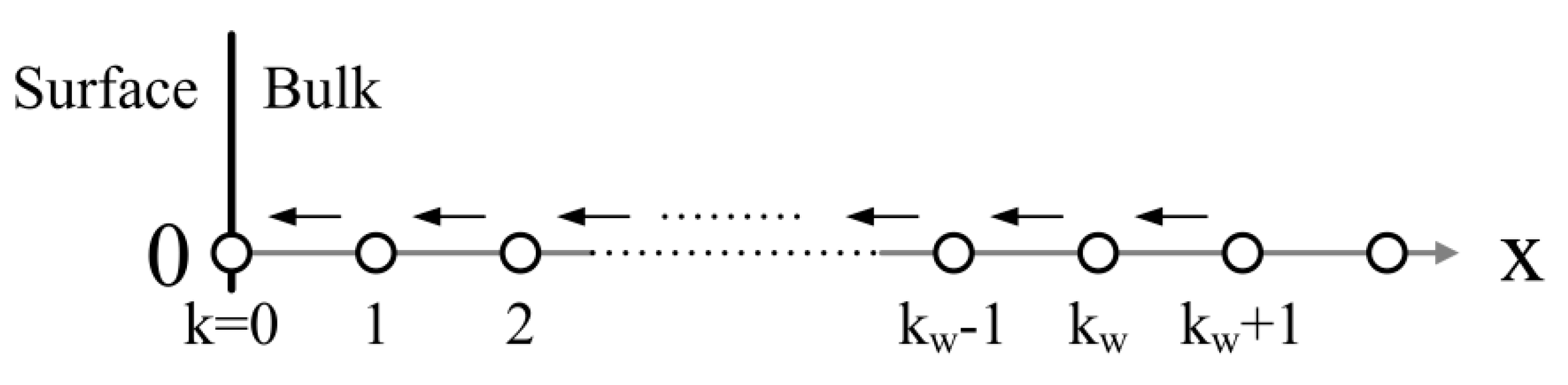
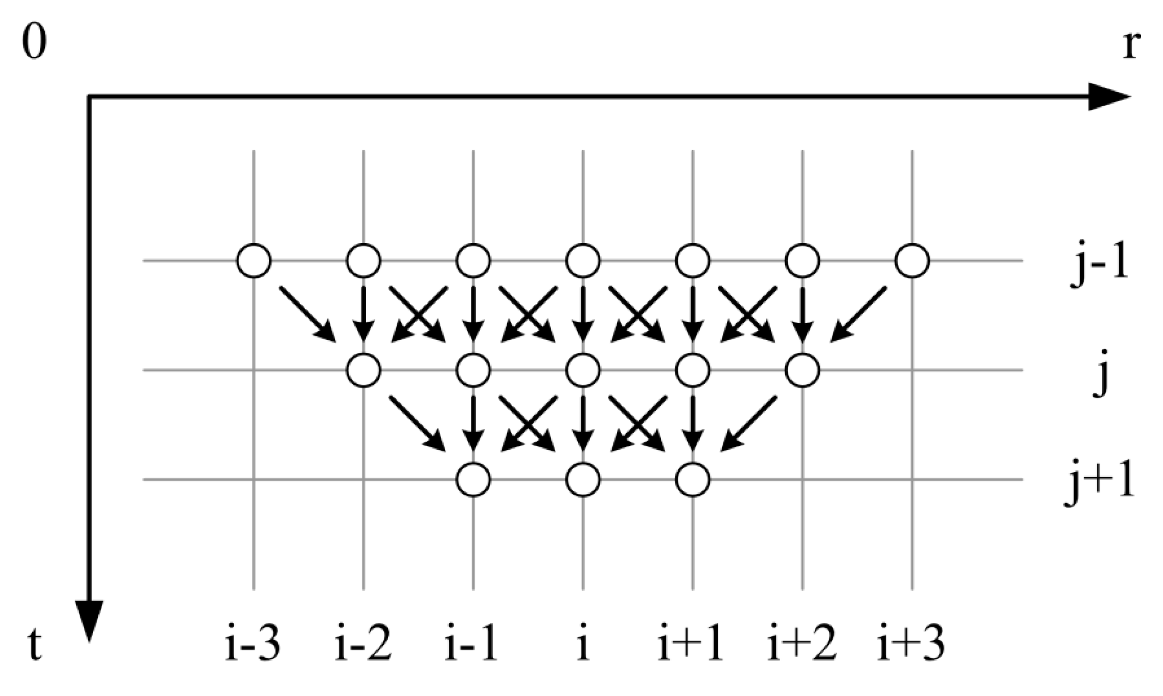
2. Methods
3. Results
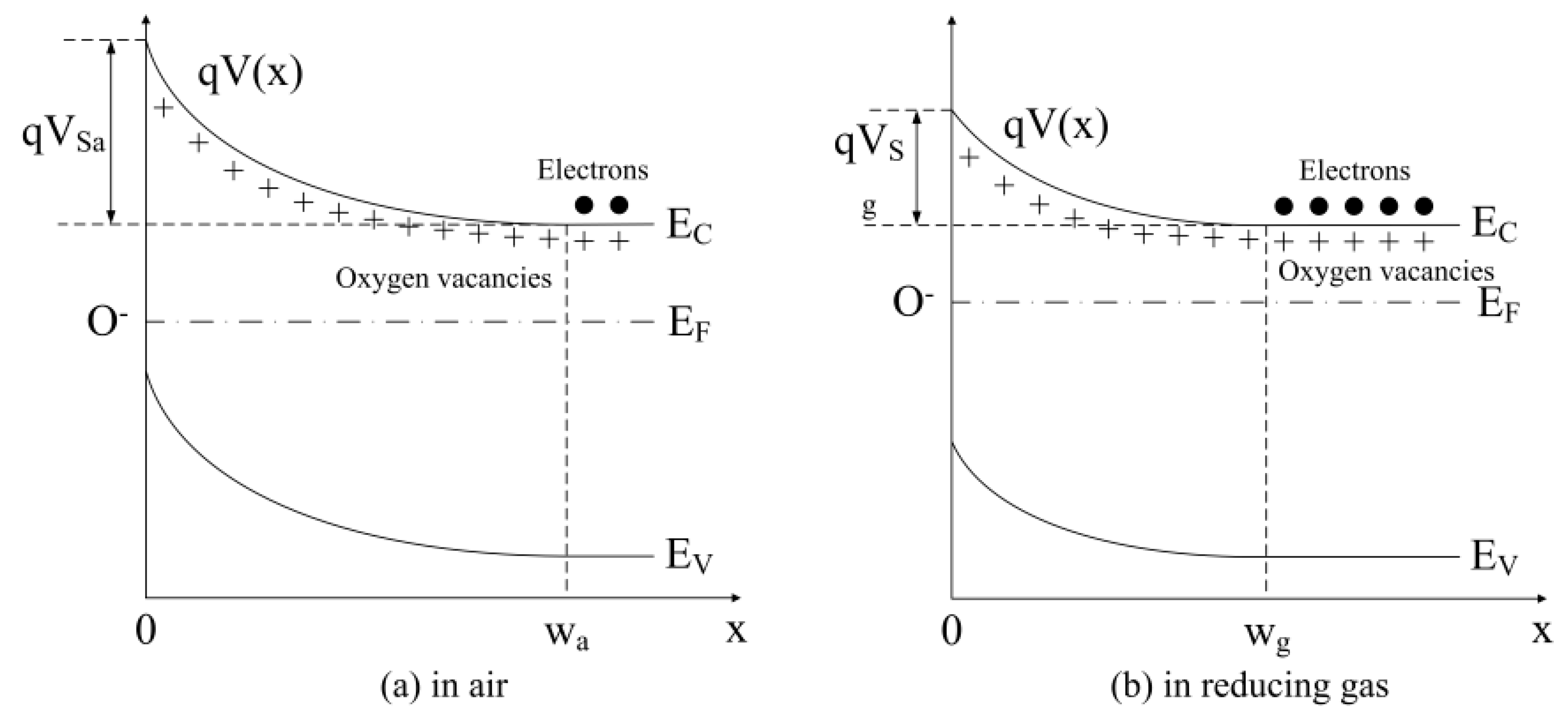
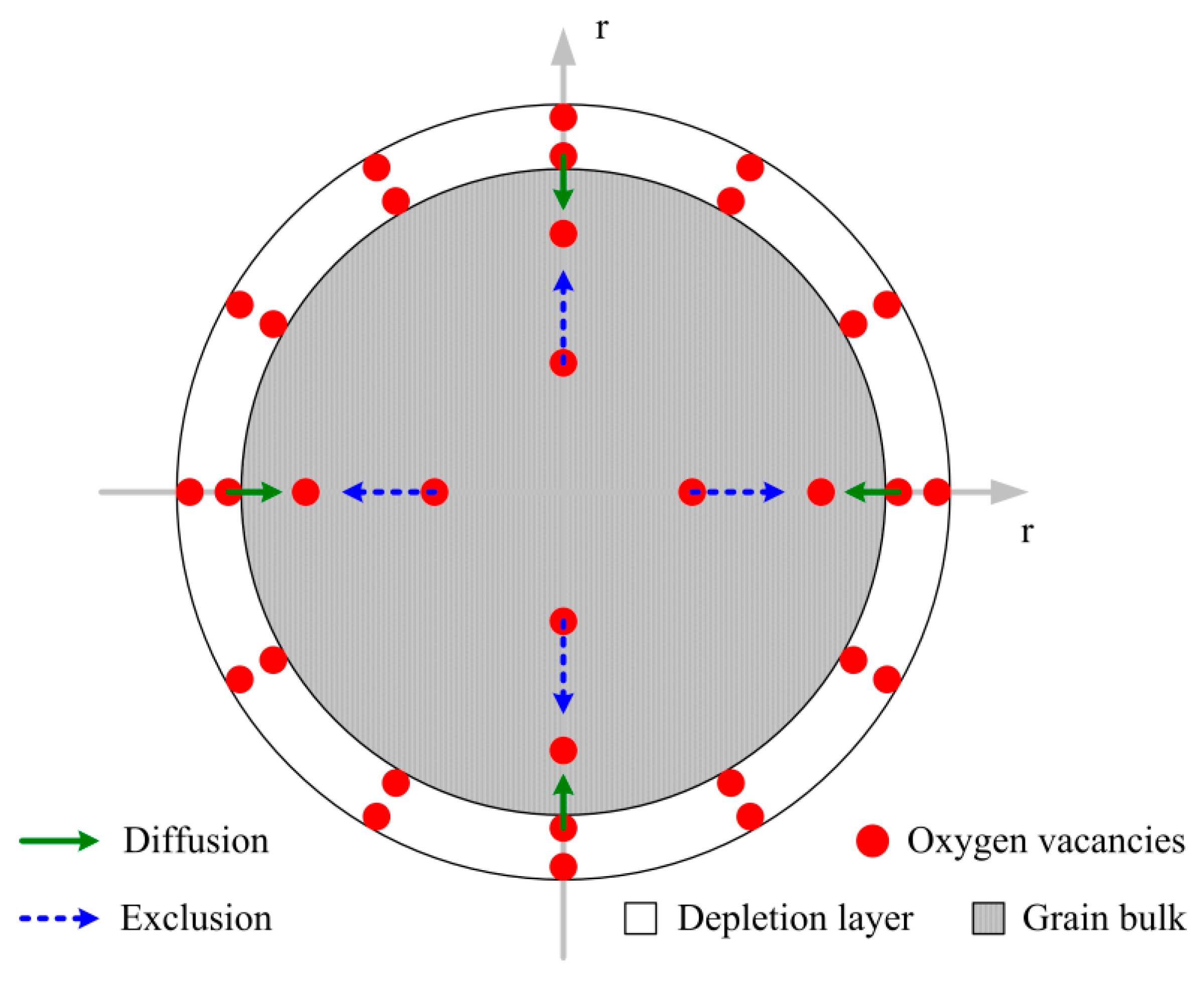
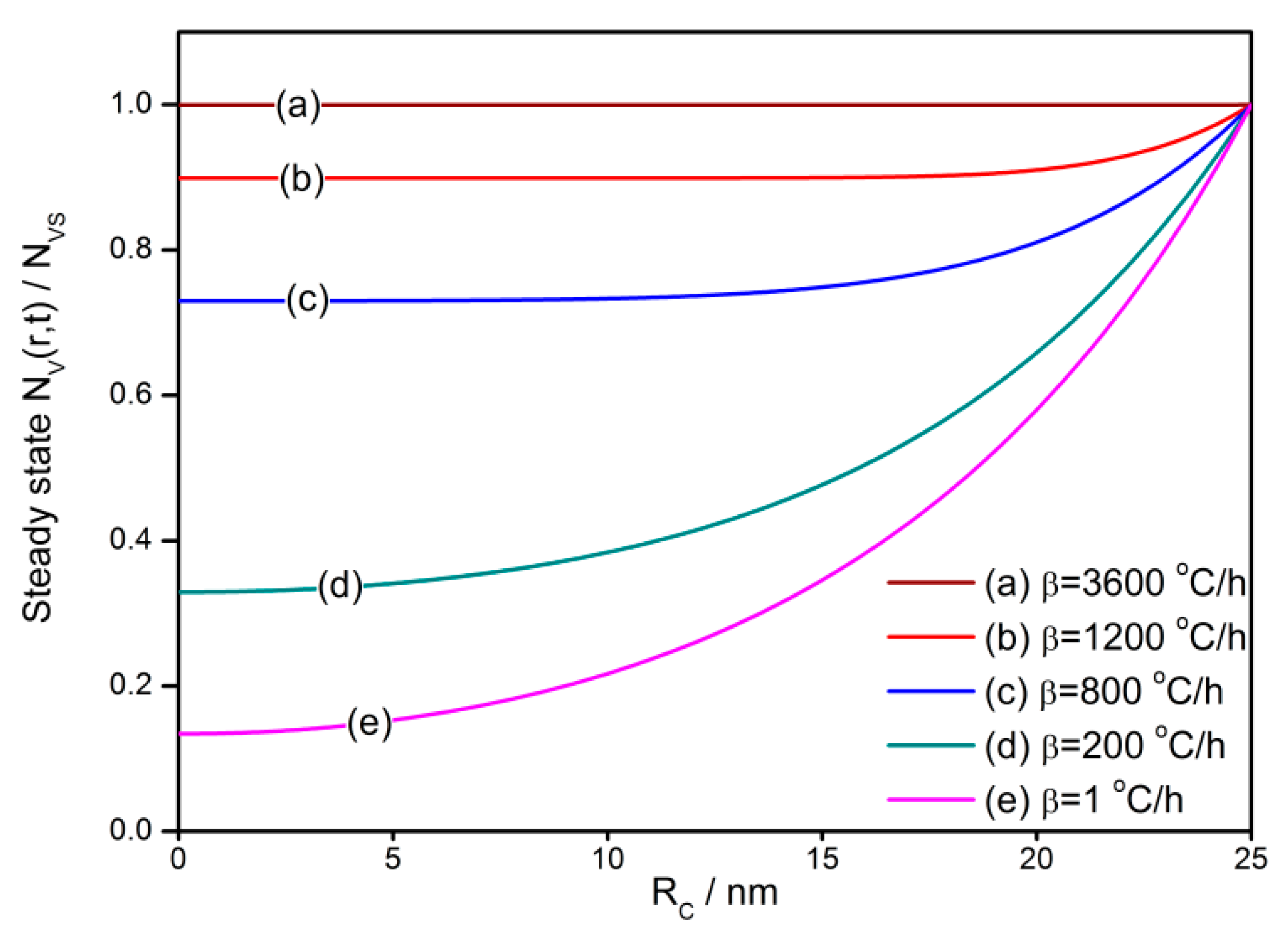
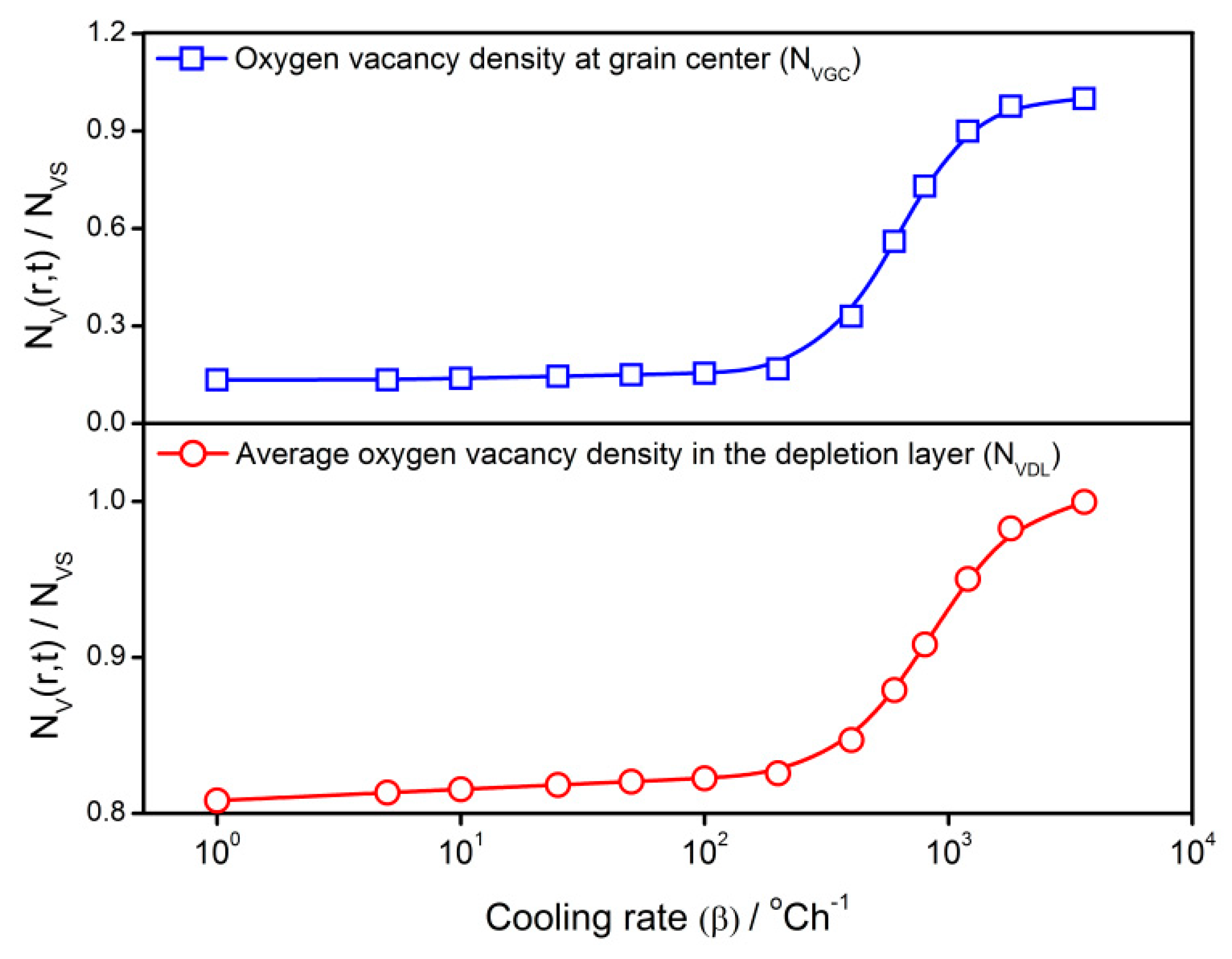
3.1. Oxygen Vacancy Distribution
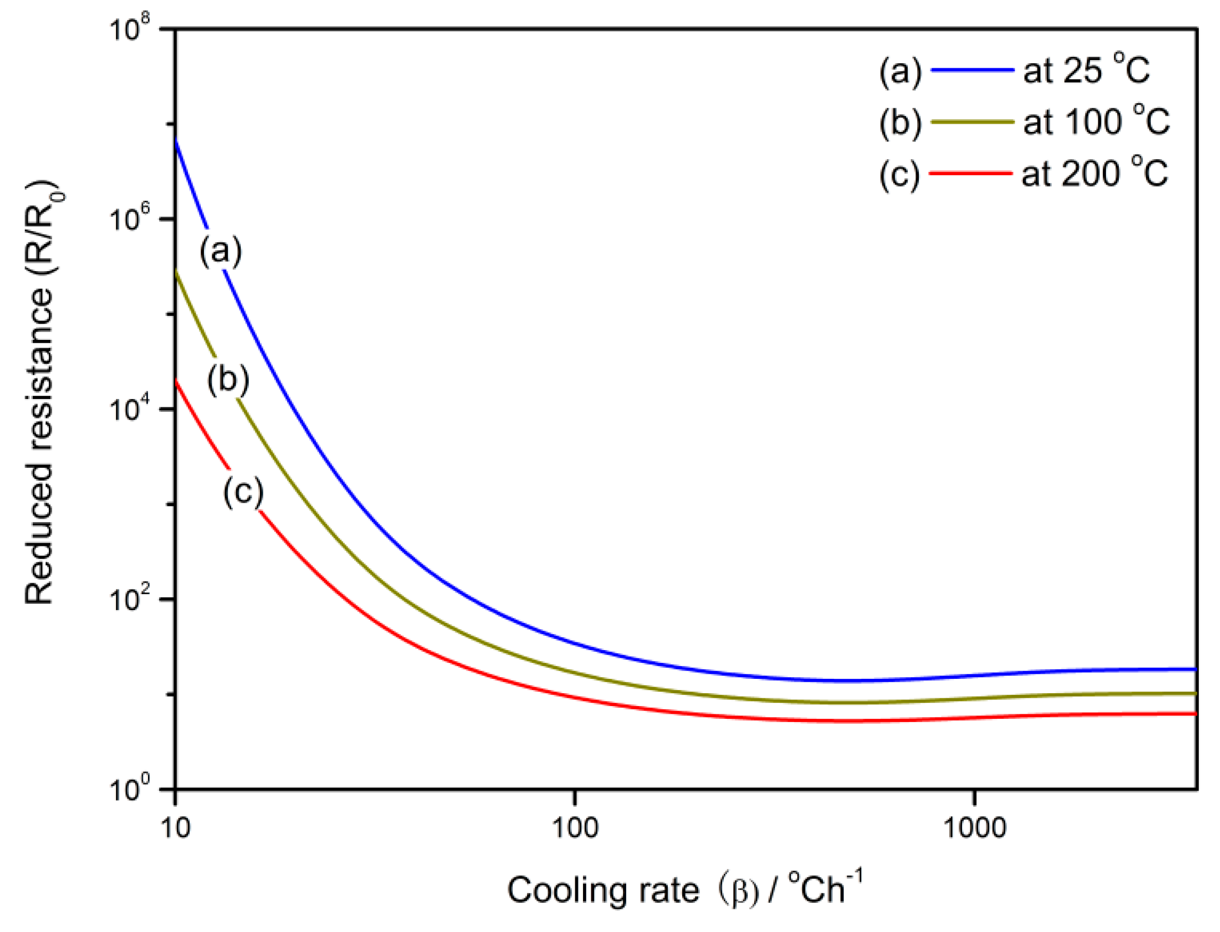
3.2. Gas-Sensing Characteristics
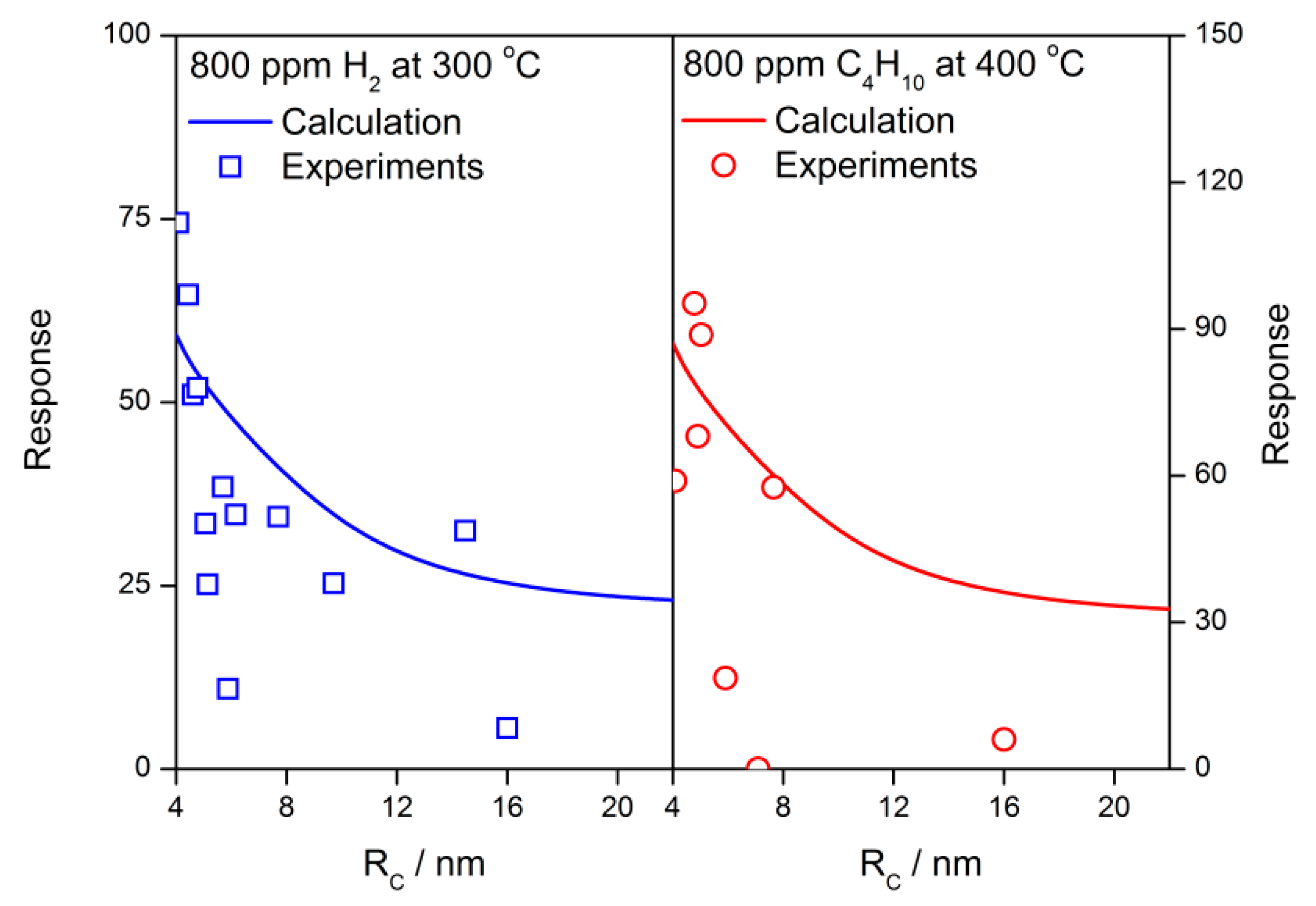
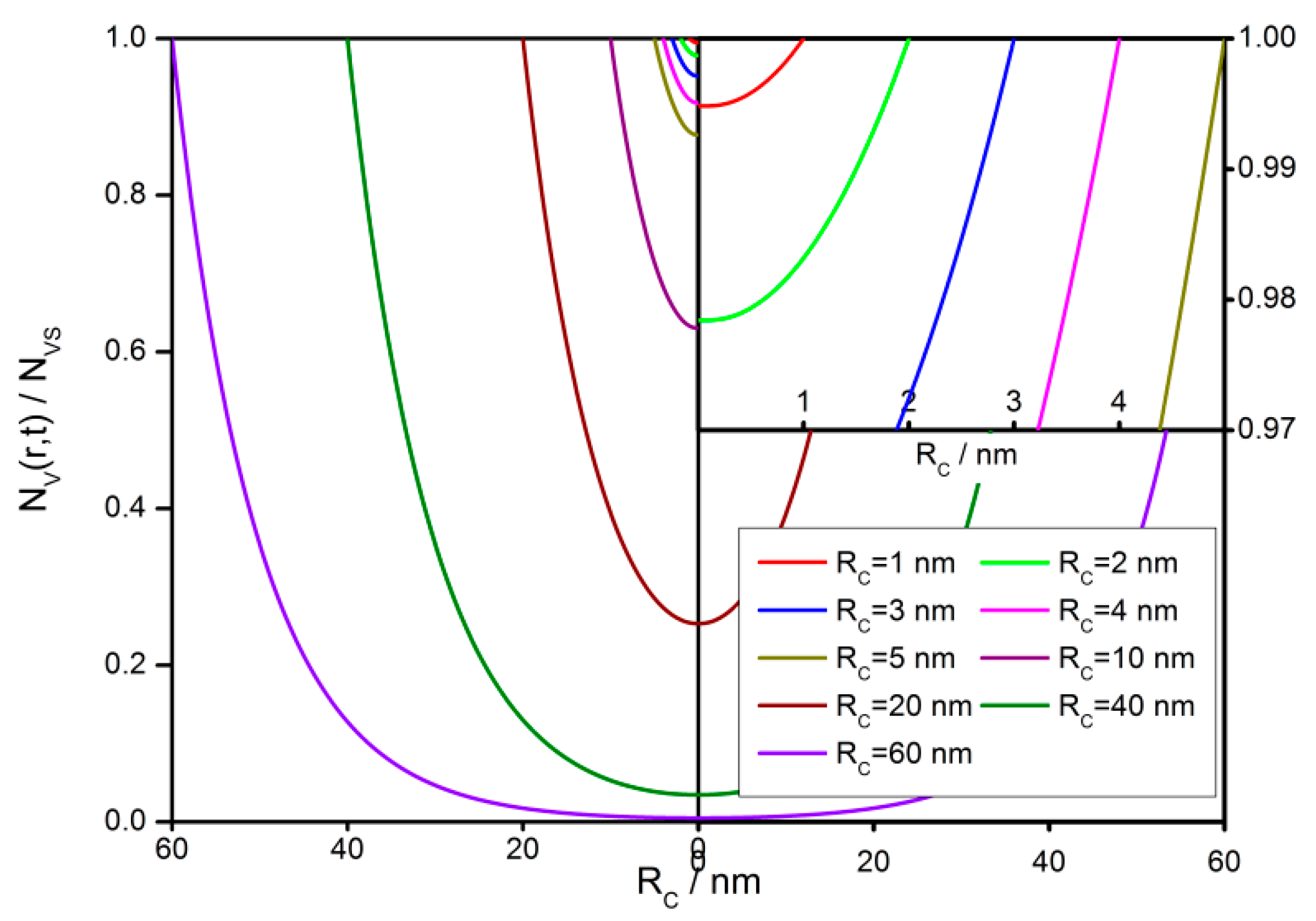
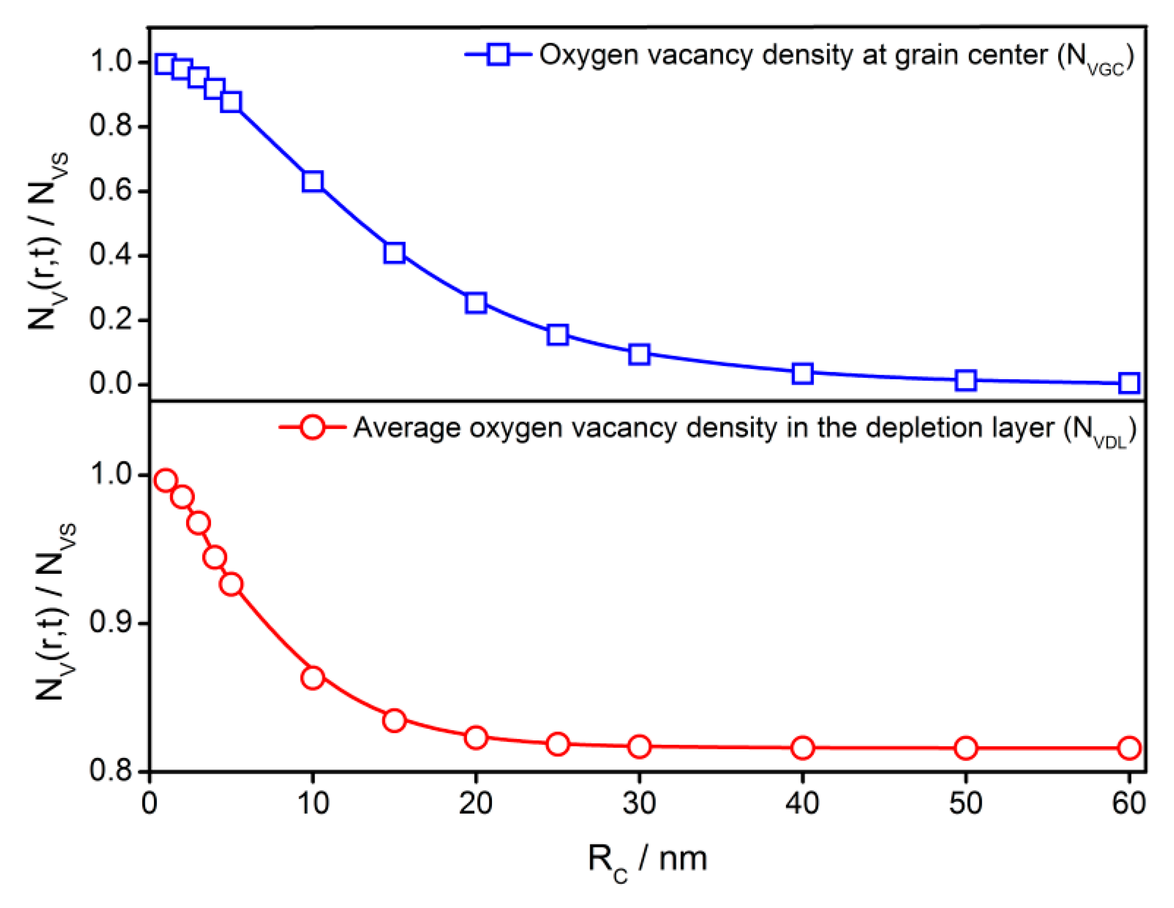
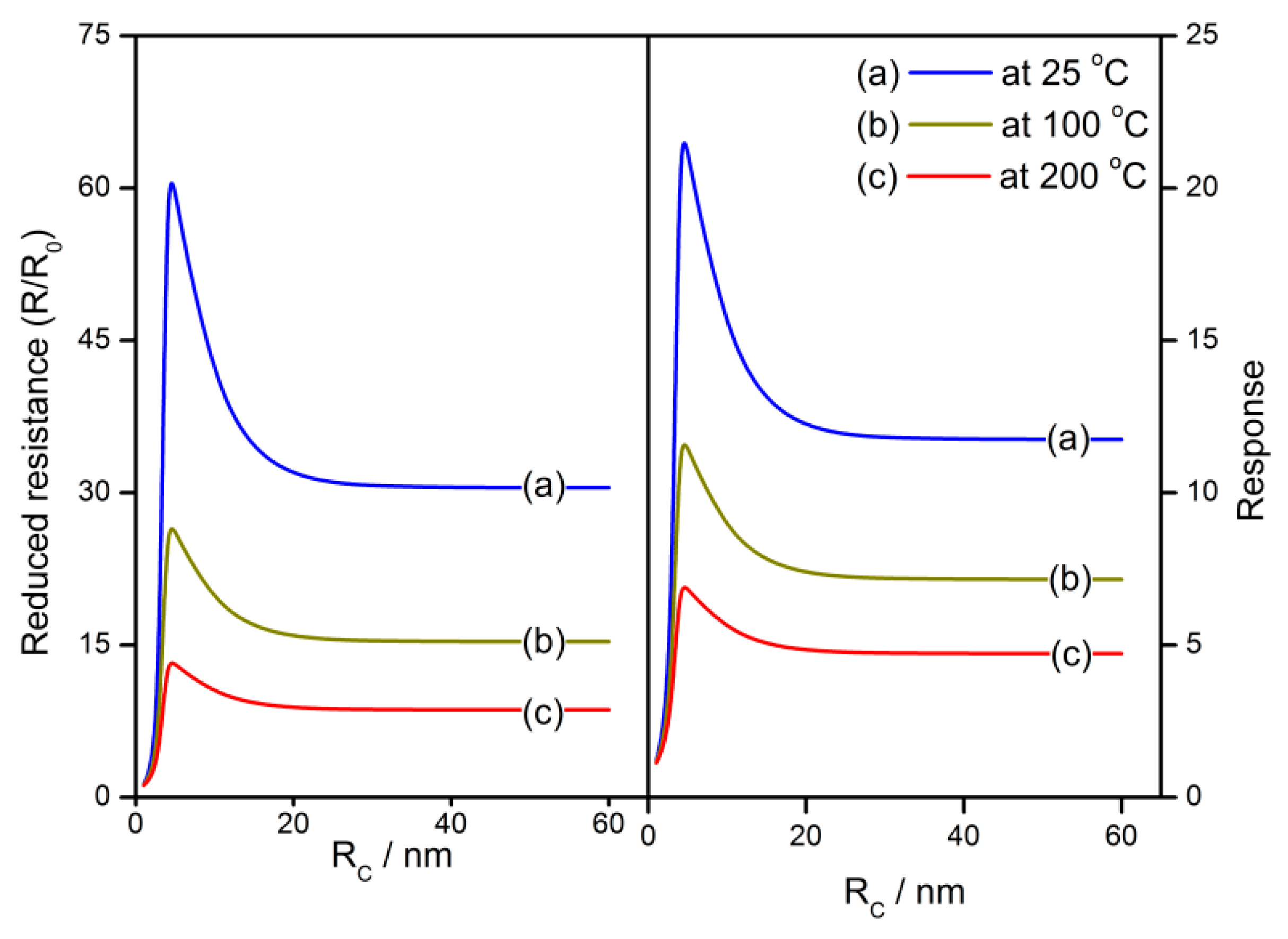
3.3. The Grain Size Effects
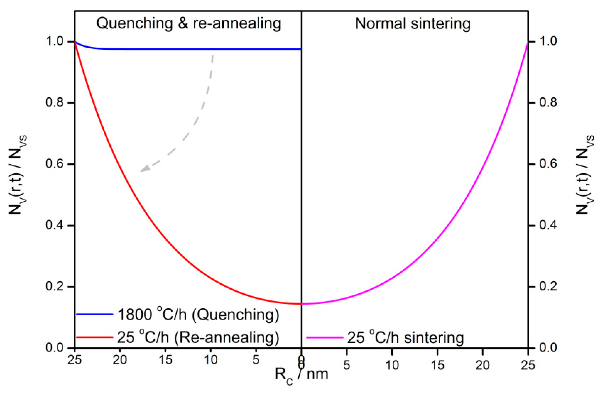
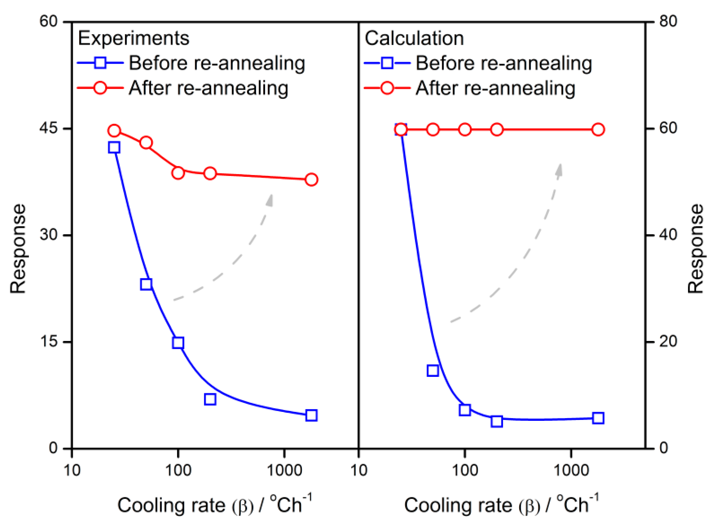
3.4. Re-Annealing Effect
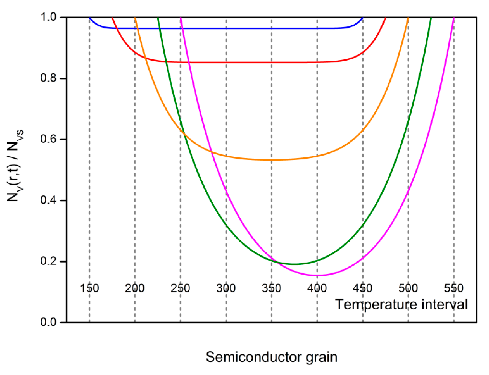
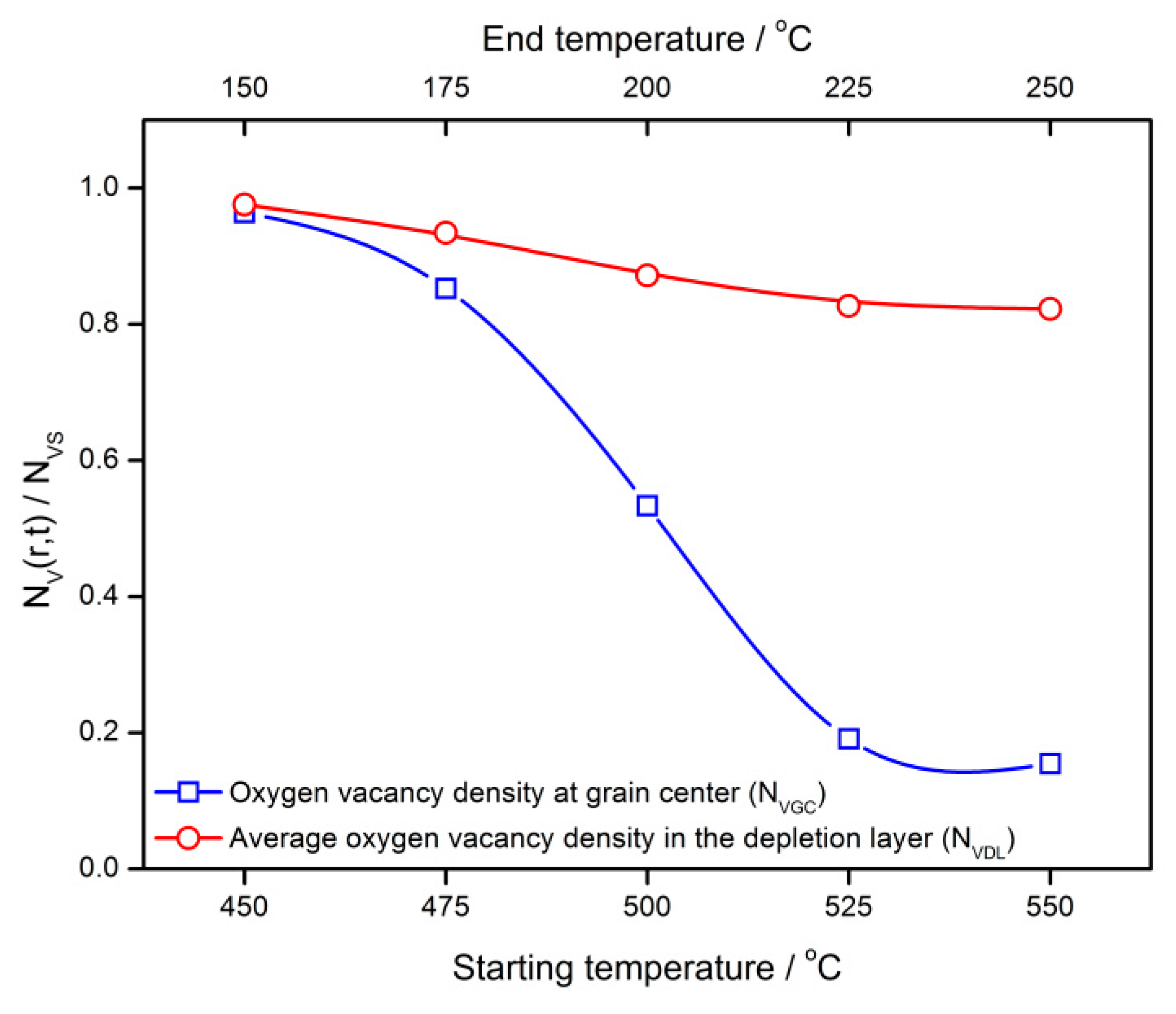
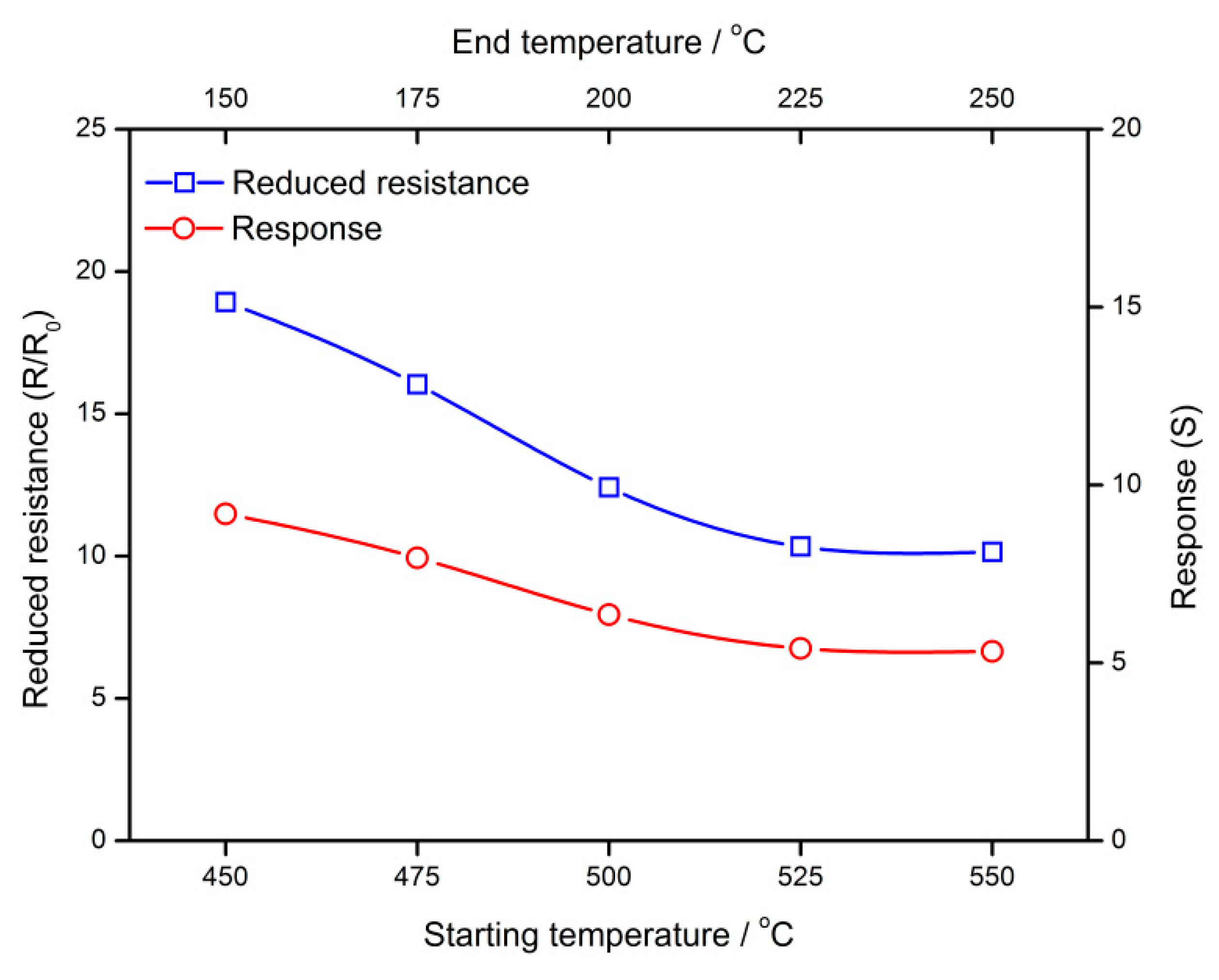
3.5. Controlled Temperature Interval
4. Discussion
5. Conclusions
- (a)
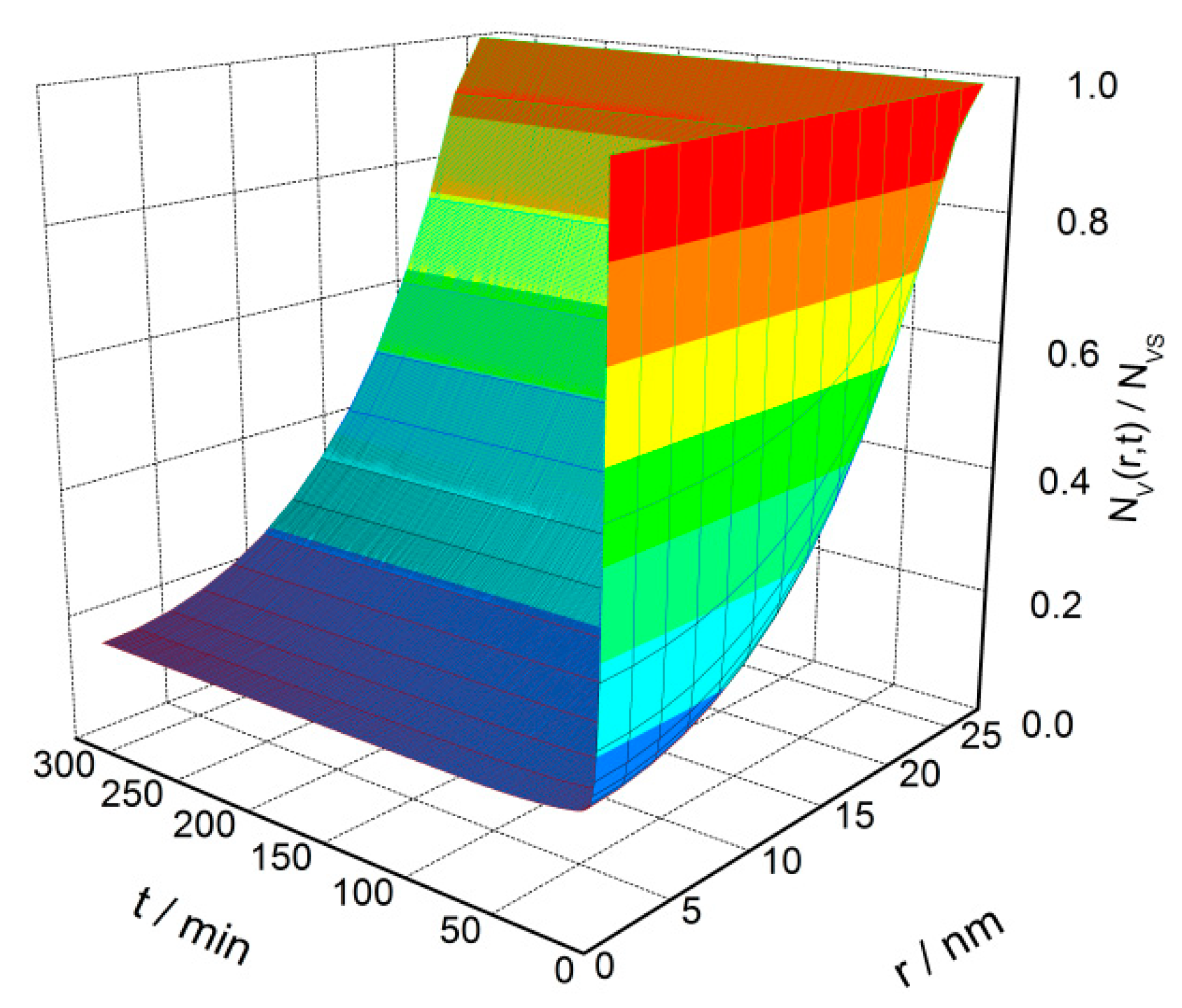
- The VO distribution profile in semiconductor grain is determined by the cooling rate in the cooling process. Quenching or fast cooling can freeze the oxygen defects at the place where they form, which may results in an almost uniform distribution. A sintering or re-annealing with a low cooling rate may lead to a gradient VO distribution. For the VO density at the grain center and average density in the depletion layer, there are two regions where the defects densities have linear correlations with the cooling rate.
- (b)
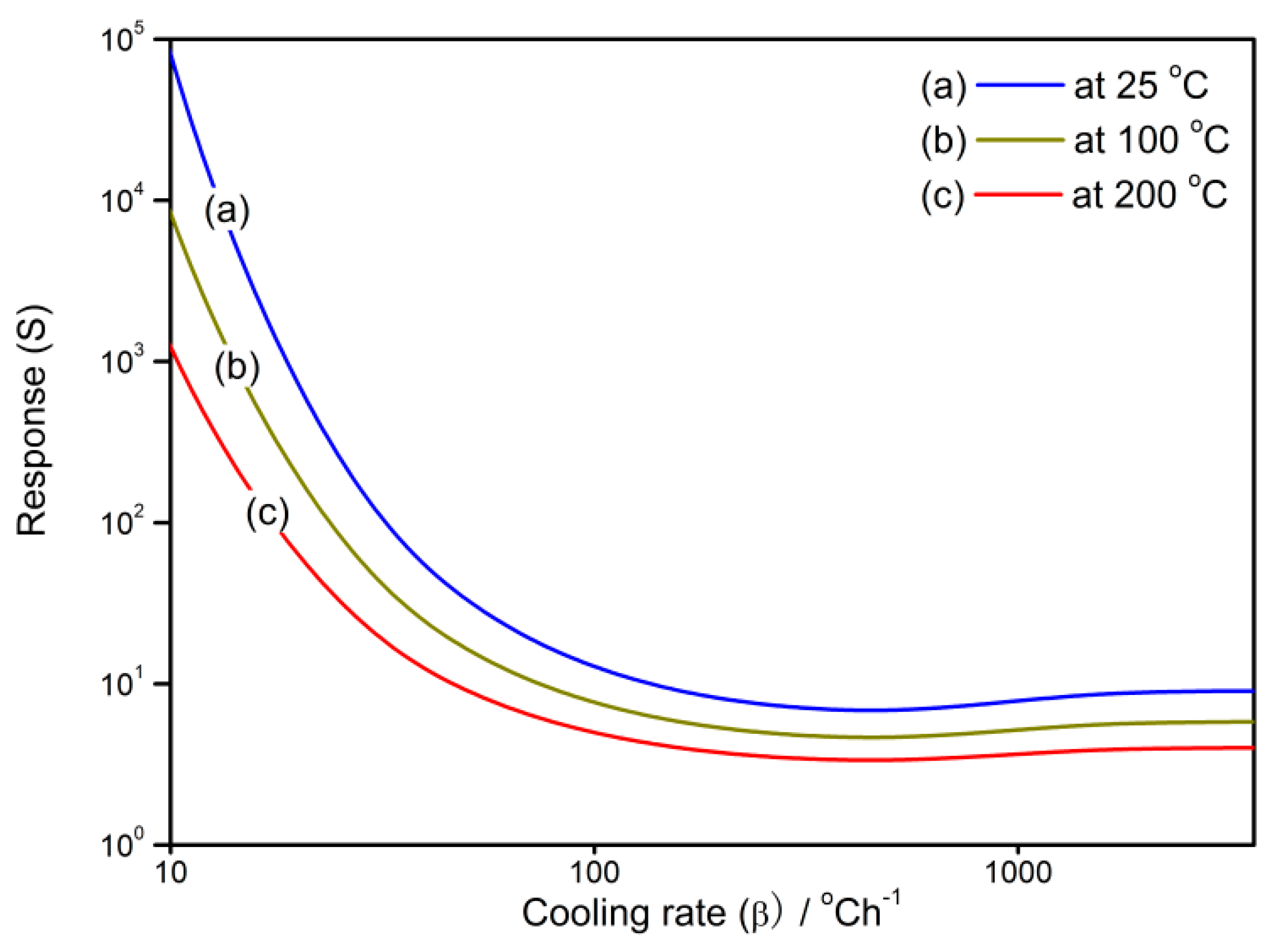
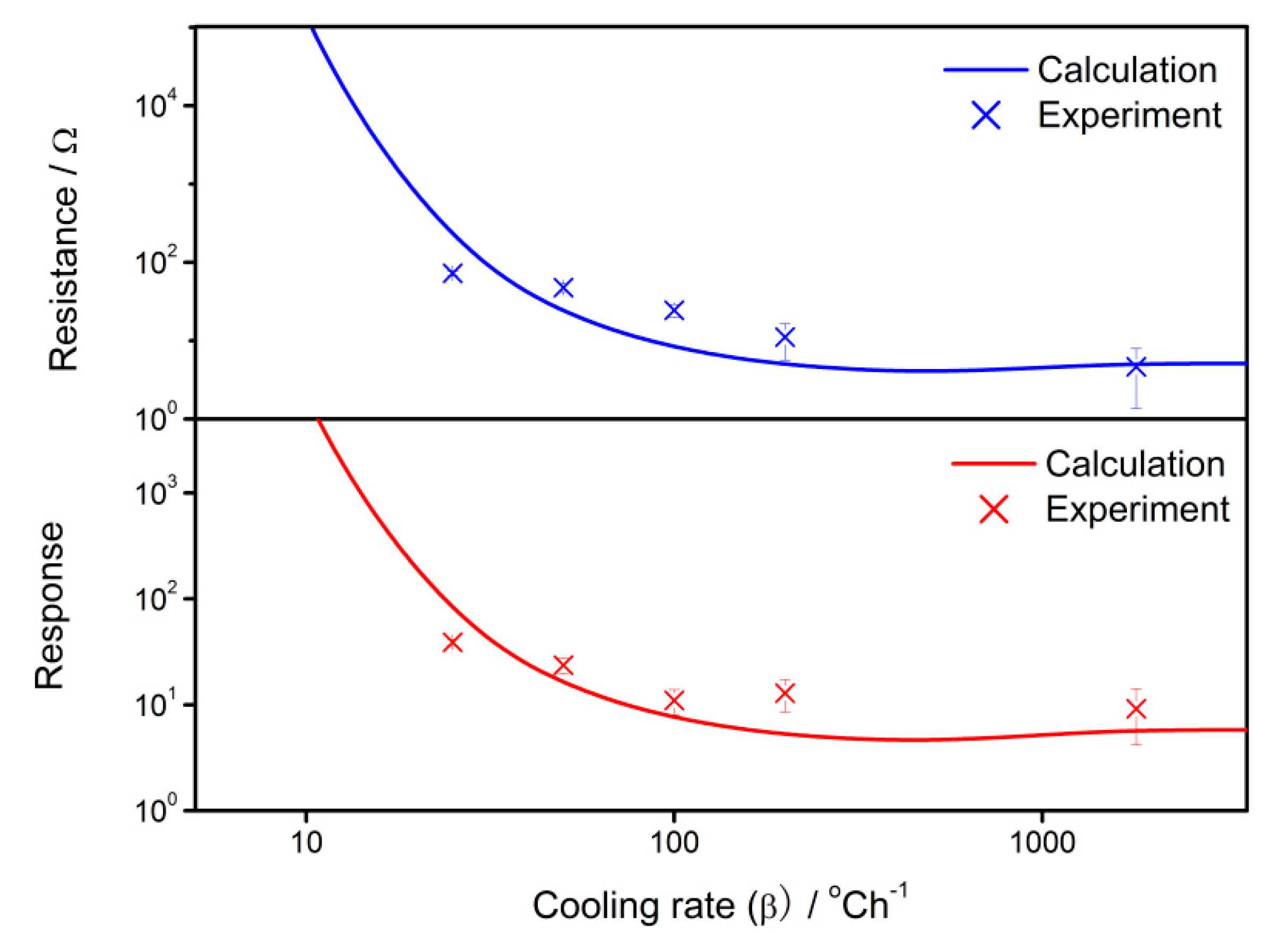
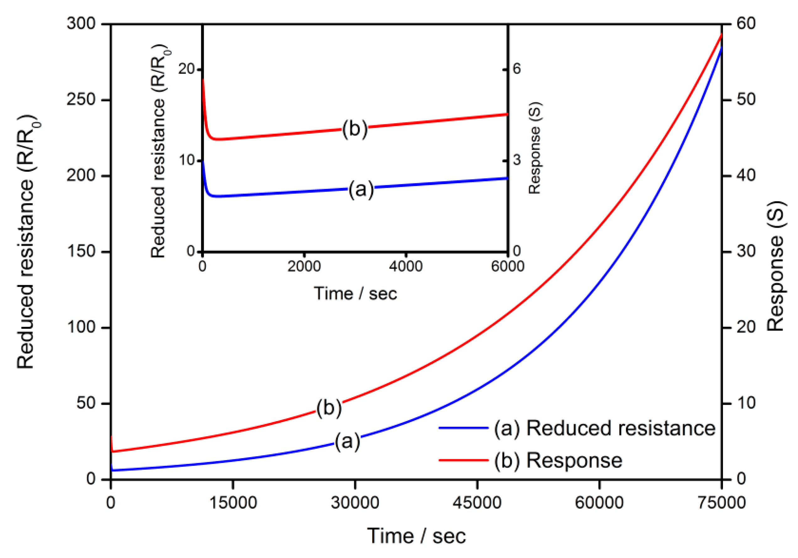
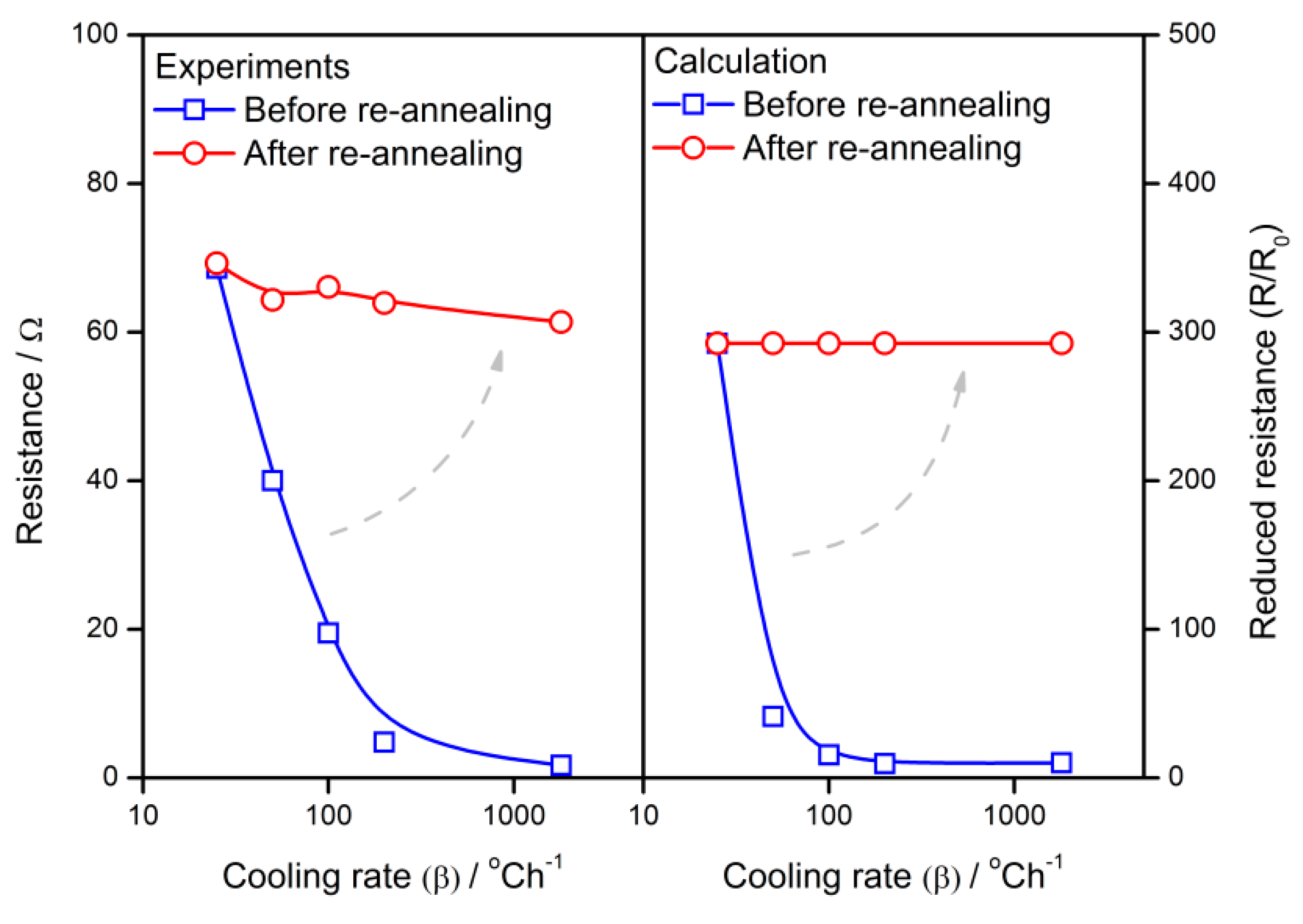
- The gas-sensing characteristics of the semiconductor correlate to the cooling rate. Negative relationships are observed for the reduced resistance and response to reducing gas against the cooling rate below 400 °C/h. The transient states of the gas-sensing properties during the cooling process show that there are sharp declines of reduced resistance and response at the starting of the cooling process. A designed re-annealing process can adjust the properties of semi-conductor gas sensors.
- (c)
- The VO distribution and gas sensor properties appear to have significant grain size effects. Large grains may maintain a great gradient of VO distribution. When the grain radius approaches the depletion layer width, the gas-sensing properties increase until they reach the maximum. After the grain is in volume depletion, the sensor loses its gas-sensing properties rapidly. The optimized gas-sensing performances appear when RC = w.
- (d)
- The cooling process in the fabrication can be designed for controlling the sensor performances, which are dependent on the temperature interval. The sensor resistance and response benefit from the low temperature treatment, which reduces the VO distribution gradient in the semiconductor grain.
Author Contributions
Funding
Conflicts of Interest
References
- Seiyama, T.; Kato, A.; Fujiishi, K.; Nagatani, M. A new detector for gaseous components using semiconductive thin films. Anal. Chem. 1962, 34, 1502–1503. [Google Scholar] [CrossRef]
- Shuping, G.; Jing, X.; Jianqiao, L.; Dongxiang, Z. Highly sensitive SnO2 thin film with low operating temperature prepared by sol-gel technique. Sens. Actuators B 2008, 134, 57–61. [Google Scholar] [CrossRef]
- Gong, S.; Liu, J.; Xia, J.; Quan, L.; Liu, H.; Zhou, D. Gas sensing characteristics of SnO2 thin films and analyses of sensor response by the gas diffusion theory. Mater. Sci. Eng. B 2009, 164, 85–90. [Google Scholar] [CrossRef]
- Zhao, J.; Wu, S.; Liu, J.; Liu, H.; Gong, S.; Zhou, D. Tin oxide thin films prepared by aerosol-assisted chemical vapor deposition and the characteristics on gas detection. Sens. Actuators B 2010, 145, 788–793. [Google Scholar] [CrossRef]
- Yu, L.; Guo, F.; Liu, S.; Yang, B.; Jiang, Y.; Qi, L.; Fan, X. Both oxygen vacancies defects and porosity facilitated NO2 gas sensing response in 2D ZnO nanowalls at room temperature. J. Alloys Compd. 2016, 682, 352–356. [Google Scholar] [CrossRef]
- Li, Z.; Qin, W.; Zhao, W.; Wu, X. Synthesis of flower-like Al doped ZnO microstructures by hydrothermal process and analysis of their gas sensing properties. Funct. Mater. Lett. 2014, 7, 1450037. [Google Scholar] [CrossRef]
- Zeng, J.; Hu, M.; Wang, W.; Chen, H.; Qin, Y. NO2-sensing properties of porous WO3 gas sensor based on anodized sputtered tungsten thin film. Sens. Actuators B 2012, 161, 447–452. [Google Scholar] [CrossRef]
- Barsan, N. Conduction models in gas-sensing SnO2 layers: Grain-size effects and ambient atmosphere influence. Sens. Actuators B 1994, 17, 241–246. [Google Scholar] [CrossRef]
- Liu, H.; Wu, S.; Gong, S.; Zhao, J.; Liu, J.; Zhou, D. Nanocrystalline In2O3-SnO2 thick films for low-temperature hydrogen sulfide detection. Ceram. Int. 2011, 37, 1889–1894. [Google Scholar] [CrossRef]
- Bârsan, N.; Hübner, M.; Weimar, U. Conduction mechanisms in SnO2 based polycrystalline thick film gas sensors exposed to CO and H2 in different oxygen backgrounds. Sens. Actuators B 2011, 157, 510–517. [Google Scholar] [CrossRef]
- Liu, J.; Lu, Y.; Cui, X.; Geng, Y.; Jin, G.; Zhai, Z. Gas-sensing properties and sensitivity promoting mechanism of Cu-added SnO2 thin films deposited by ultrasonic spray pyrolysis. Sens. Actuators B 2017, 248, 862–867. [Google Scholar] [CrossRef]
- Zhao, X.; Shi, W.; Mu, H.; Xie, H.; Liu, F. Templated bicontinuous tin oxide thin film fabrication and the NO2 gas sensing. J. Alloys Compd. 2016, 659, 60–65. [Google Scholar] [CrossRef]
- Lee, Y.; Huang, H.; Tan, O.; Tse, M. Semiconductor gas sensor based on Pd-doped SnO2 nanorod thin films. Sens. Actuators B 2008, 132, 239–242. [Google Scholar] [CrossRef]
- Li, M.; Zhou, D.; Zhao, J.; Zheng, Z.; He, J.; Hu, L.; Xia, Z.; Tang, J.; Liu, H. Resistive gas sensors based on colloidal quantum dot (CQD) solids for hydrogen sulfide detection. Sens. Actuators B 2015, 217, 198–201. [Google Scholar] [CrossRef]
- Yu, H.; Song, Z.; Liu, Q.; Ji, X.; Liu, J.; Xu, S.; Kan, H.; Zhang, B.; Liu, J.; Jiang, J.; et al. Colloidal synthesis of tungsten oxide quantum dots for sensitive and selective H2S gas detection. Sens. Actuator B Chem. 2017, 248, 1029–1036. [Google Scholar] [CrossRef]
- Zhang, B.; Li, M.; Song, Z.; Kan, H.; Yu, H.; Liu, Q.; Zhang, G.; Liu, H. Sensitive H2S gas sensors employing colloidal zinc oxide quantum dots. Sens. Actuators B 2017, 249, 558–563. [Google Scholar] [CrossRef]
- Morrison, S.R. Mechanism of semiconductor gas sensor operation. Sens. Actuators 1987, 11, 283–287. [Google Scholar] [CrossRef]
- Yamazoe, N.; Shimanoe, K. Theory of power laws for semiconductor gas sensors. Sens. Actuators B 2008, 128, 566–573. [Google Scholar] [CrossRef]
- Yamazoe, N.; Shimanoe, K. New perspectives of gas sensor technology. Sens. Actuators B 2009, 138, 100–107. [Google Scholar] [CrossRef]
- Tamaki, J.; Zhang, Z.; Fujimori, K.; Akiyama, M.; Harada, T.; Miura, N.; Yamazoe, N. Grain-size effects in tungsten oxide-based sensor for nitrogen oxides. J. Electrochem. Soc. 1994, 141, 2207–2210. [Google Scholar] [CrossRef]
- Yamazoe, N.; Shimanoe, K. Roles of shape and size of component crystals in semiconductor gas sensors I. Response to oxygen. J. Electrochem. Soc. 2008, 155, J85–J92. [Google Scholar] [CrossRef]
- Yamazoe, N.; Shimanoe, K. Roles of shape and size of component crystals in semiconductor gas sensors II. Response to NO2 and H2. J. Electrochem. Soc. 2008, 155, J93–J98. [Google Scholar] [CrossRef]
- Korotcenkov, G.; Brinzari, V.; Boris, Y.; Ivanov, M.; Schwank, J.; Morante, J. Influence of surface Pd doping on gas sensing characteristics of SnO2 thin films deposited by spray pirolysis. Thin Solid Films 2003, 436, 119–126. [Google Scholar] [CrossRef]
- Gupta, V.; Mozumdar, S.; Chowdhuri, A.; Sreenivas, K. Influence of CuO catalyst in the nanoscale range on SnO2 surface for H2S gas sensing applications. Pramana 2005, 65, 647–652. [Google Scholar] [CrossRef]
- Yamazoe, N.; Fuchigami, J.; Kishikawa, M.; Seiyama, T. Interactions of tin oxide surface with O2, H2O and H2. Surf. Sci. 1979, 86, 335–344. [Google Scholar] [CrossRef]
- Liu, H.; Gong, S.; Hu, Y.; Liu, J.; Zhou, D. Properties and mechanism study of SnO2 nanocrystals for H2S thick-film sensors. Sens. Actuators B 2009, 140, 190–195. [Google Scholar] [CrossRef]
- Wu, J.; Huang, Q.; Zeng, D.; Zhang, S.; Yang, L.; Xia, D.; Xiong, Z.; Xie, C. Al-doping induced formation of oxygen-vacancy for enhancing gas-sensing properties of SnO2 NTs by electrospinning. Sens. Actuators B 2014, 198, 62–69. [Google Scholar] [CrossRef]
- Zou, C.; Liang, F.; Xue, S. Synthesis and oxygen vacancy related NO2 gas sensing properties of ZnO: Co nanorods arrays gown by a hydrothermal method. Appl. Surf. Sci. 2015, 353, 1061–1069. [Google Scholar] [CrossRef]
- Morrison, S.R. Semiconductor gas sensors. Sens. Actuators 1982, 2, 329–341. [Google Scholar] [CrossRef]
- Ge, Y.; Wei, Z.; Li, Y.; Qu, J.; Zu, B.; Dou, X. Highly sensitive and rapid chemiresistive sensor towards trace nitro-explosive vapors based on oxygen vacancy-rich and defective crystallized In-doped ZnO. Sens. Actuators B 2017, 244, 983–991. [Google Scholar] [CrossRef]
- Liu, J.; Gao, Y.; Wu, X.; Jin, G.; Zhai, Z.; Liu, H. Inhomogeneous oxygen vacancy distribution in semiconductor gas sensors: Formation, migration and determination on gas sensing characteristics. Sensors 2017, 17, 1852. [Google Scholar] [CrossRef] [PubMed]
- Zhang, C.; Geng, X.; Li, J.; Luo, Y.; Lu, P. Role of oxygen vacancy in tuning of optical, electrical and NO2 sensing properties of ZnO1-X coatings at room temperature. Sens. Actuators B 2017, 248, 886–893. [Google Scholar] [CrossRef]
- Liu, J.; Gong, S.; Fu, Q.; Wang, Y.; Quan, L.; Deng, Z.; Chen, B.; Zhou, D. Time-dependent oxygen vacancy distribution and gas sensing characteristics of tin oxide gas sensitive thin films. Sens. Actuators B 2010, 150, 330–338. [Google Scholar] [CrossRef]
- Liu, J.; Gong, S.; Quan, L.; Deng, Z.; Liu, H.; Zhou, D. Influences of cooling rate on gas sensitive tin oxide thin films and a model of gradient distributed oxygen vacancies in SnO2 crystallites. Sens. Actuators B 2010, 145, 657–666. [Google Scholar] [CrossRef]
- Shimizu, Y.; Kobayashi, N.; Uedono, A.; Okada, Y. Improvement of crystal quality of GaInNAs films grown by atomic hydrogen-assisted RF-MBE. J. Cryst. Growth 2005, 278, 553–557. [Google Scholar] [CrossRef]
- Zhang, M.; Lin, C.; Weng, H.; Scholz, R.; Gösele, U. Defect distribution and evolution in He+ implanted Si studied by variable-energy positron beam. Thin Solid Films 1998, 333, 245–250. [Google Scholar] [CrossRef]
- Sze, S.M.; Ng, K.K. Physics of Semiconductor Devices, 3rd ed.; John Wiley & Sons, Inc.: Hoboken, NJ, USA, 2006. [Google Scholar]
- Liu, J.; Zhai, Z.; Jin, G.; Li, Y.; Monica, F.F.; Liu, X. Simulation of the grain size effect in gas-sensitive SnO2 thin films using the oxygen vacancy gradient distribution model. Electron. Mater. Lett. 2015, 11, 34–40. [Google Scholar] [CrossRef]
- Maier, J.; Göpel, W. Investigations of the bulk defect chemistry of polycrystalline tin (IV) oxide. J. Solid State Chem. 1988, 72, 293–302. [Google Scholar] [CrossRef]
- Kittel, C. Introduction to Solid State Physics; John Wiley & Sons, Inc.: New York, NY, USA, 2004. [Google Scholar]
- Liu, J.; Liu, X.; Zhai, Z.; Jin, G.; Jiang, Q.; Zhao, Y.; Luo, C.; Quan, L. Evaluation of depletion layer width and gas-sensing properties of antimony-doped tin oxide thin film sensors. Sens. Actuators B 2015, 220, 1354–1360. [Google Scholar] [CrossRef]
- Liu, J.; Jin, G.; Zhai, Z.; Monica, F.F.; Liu, X. Numeral description of grain size effects of tin oxide gas-sensitive elements and evaluation of depletion layer width. Electron. Mater. Lett. 2015, 11, 457–465. [Google Scholar] [CrossRef]
- Xu, C.; Tamaki, J.; Miura, N.; Yamazoe, N. Grain size effects on gas sensitivity of porous SnO2-based elements. Sens. Actuators B 1991, 3, 147–155. [Google Scholar] [CrossRef]
- Liu, J.; Lu, Y.; Cui, X.; Jin, G.; Zhai, Z. Effect of depletion layer width on electrical properties of semiconductive thin film gas sensor: A numerical study based on the gradient-distributed oxygen vacancy model. Appl. Phys. A 2016, 122, 146. [Google Scholar] [CrossRef]


© 2018 by the authors. Licensee MDPI, Basel, Switzerland. This article is an open access article distributed under the terms and conditions of the Creative Commons Attribution (CC BY) license (http://creativecommons.org/licenses/by/4.0/).
Share and Cite
Liu, J.; Wang, W.; Zhai, Z.; Jin, G.; Chen, Y.; Hong, W.; Wu, L.; Gao, F. Influence of Oxygen Vacancy Behaviors in Cooling Process on Semiconductor Gas Sensors: A Numerical Analysis. Sensors 2018, 18, 3929. https://doi.org/10.3390/s18113929
Liu J, Wang W, Zhai Z, Jin G, Chen Y, Hong W, Wu L, Gao F. Influence of Oxygen Vacancy Behaviors in Cooling Process on Semiconductor Gas Sensors: A Numerical Analysis. Sensors. 2018; 18(11):3929. https://doi.org/10.3390/s18113929
Chicago/Turabian StyleLiu, Jianqiao, Wanqiu Wang, Zhaoxia Zhai, Guohua Jin, Yuzhen Chen, Wusong Hong, Liting Wu, and Fengjiao Gao. 2018. "Influence of Oxygen Vacancy Behaviors in Cooling Process on Semiconductor Gas Sensors: A Numerical Analysis" Sensors 18, no. 11: 3929. https://doi.org/10.3390/s18113929
APA StyleLiu, J., Wang, W., Zhai, Z., Jin, G., Chen, Y., Hong, W., Wu, L., & Gao, F. (2018). Influence of Oxygen Vacancy Behaviors in Cooling Process on Semiconductor Gas Sensors: A Numerical Analysis. Sensors, 18(11), 3929. https://doi.org/10.3390/s18113929