Abstract
This paper proposes a novel charge-based Complementary Metal Oxide Semiconductor (CMOS) capacitive sensor for life science applications. Charge-based capacitance measurement (CBCM) has significantly attracted the attention of researchers for the design and implementation of high-precision CMOS capacitive biosensors. A conventional core-CBCM capacitive sensor consists of a capacitance-to-voltage converter (CVC), followed by a voltage-to-digital converter. In spite of their high accuracy and low complexity, their input dynamic range (IDR) limits the advantages of core-CBCM capacitive sensors for most biological applications, including cellular monitoring. In this paper, after a brief review of core-CBCM capacitive sensors, we address this challenge by proposing a new current-mode core-CBCM design. In this design, we combine CBCM and current-controlled oscillator (CCO) structures to improve the IDR of the capacitive readout circuit. Using a 0.18 μm CMOS process, we demonstrate and discuss the Cadence simulation results to demonstrate the high performance of the proposed circuitry. Based on these results, the proposed circuit offers an IDR ranging from 873 aF to 70 fF with a resolution of about 10 aF. This CMOS capacitive sensor with such a wide IDR can be employed for monitoring cellular and molecular activities that are suitable for biological research and clinical purposes.
1. Introduction
Capacitive sensors have been receiving much attention due to their high resolution, low complexity, and low temperature-dependency. Among competing sensing technologies, CMOS, by offering a distinct cost and highly integrated circuits, offers great advantages for the development of capacitive sensors. These advantages include higher sensitivity, rapid detection, and the integration of electrical readout circuits and sensing electrodes on a single chip. In spite of microelectromechanical systems (MEMS)-based capacitive sensors such as accelerometers [1,2], position sensors [3,4], pressure sensors [5,6,7,8], and moisture sensors [9], a growing body of literature has studied capacitive sensors for Laboratory on a Chip (LoC) applications. These applications include DNA hybridization detection [10], protein interactions quantification [11], cellular monitoring [12,13,14], bio-particle detection [15], microRNA detection [16], organic solvent monitoring [17], sensing of droplet parameters [18], and bacteria detection [19,20].
A capacitive sensor consists of sensing electrodes that are connected to an interface readout circuit, as shown in Figure 1a,b for both MEMS-based and LoC applications, respectively. The capacitive electrodes convert the physical [3,4], biological [10,11,12], and/or chemical parameters [21,22] in proximity of the electrodes into electrical signals. As illustrated in Figure 1a, the capacitive electrodes in MEMS-based applications such as accelerometers are used as an off-chip device wire-bonded (or flip-chip bonded) to the CMOS chip. For LoC applications, the sensing electrodes are realized above CMOS chip (see Figure 1b). The capacitive interface circuits are used to convert these signals into voltage, frequency, or other digital data [10,20,23,24]. A readout interface is required to accurately detect and process the sensed signals by electrodes. In CMOS-based lab-on-chip applications, microfluidic structures are implemented above CMOS sensing chips for steering biochemical samples through sensing electrodes. In these structures, various materials such as silicon, glass, and polymers can be formed using photolithography techniques [25,26,27]. Among them, polydimethylsiloxane (PDMS), SU-8, and polymethyl methacrylate are widely used for the development of low-cost disposable microfluidic structures. In addition to conventional high precision lithography, other techniques can also be utilized to fabricate microfluidic structures. These techniques include hot embossing [28], microinjection molding [29], soft lithography [30], photo-ablation [31], LIGA [32], 3D printing [33], and direct-write fabrication process (DWFP) [34]. In the development of hybrid microfluidic-CMOS systems, the biocompatibility and the reliability of the microfluidic packaging will be considered as key challenging issues. These challenges have been addressed by several researchers [30,34,35,36,37,38,39,40,41,42].
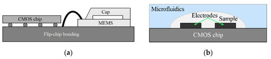
Figure 1.
(a) Conceptual view of wire-bonded electrodes used for microelectromechanical systems (MEMS) applications, (b) conceptual view of on-chip electrodes used for Laboratory on a Chip (LoC) applications.
There is a considerable amount of literature on CMOS capacitive sensors for different LoC applications [12,15,20,23,24,43,44] using various circuitry methods. These methods include charge redistribution method (ChR), capacitance-to-frequency conversion (C2F), lock-in detection, and charge-based capacitance measurement (CBCM).
Charge redistribution methods (ChR): Capacitive sensors may work based on charge redistribution principles using charge sharing (ChS) approaches [13,20], charge sensitive amplifiers (CSA) [45,46], or switched capacitor (SC) circuits [15,24,47]. In the charge sharing method, the voltage of a capacitor with known capacitance is proportional to the sensing capacitor whose charge is redistributed to the known capacitor using proper switches. The charge sharing circuit proposed in [20] occupies a small area, about 0.1 mm2 for a 16 × 16 array of sensor, but it has a limited sensitivity in comparison to the other sensors. In the charge sensitive amplifier-based methods, the readout circuit consists of a sensing and a reference capacitor, and an integrator, including an operational amplifier and an integrating feedback capacitor. A switch is also used to reset the voltage of the feedback capacitor. The output voltage of the amplifier is representative of the difference between the reference and sensing capacitances. A high resolution can be achieved using a charge sensitive amplifier as in [15] (about 21 aF for this example). In contrast to charge-sensitive amplifiers, which are controlled by voltage pulses, switched capacitor circuits use switches for charging and discharging capacitors. These circuits suffer offset, charge injection, and switching problems. Techniques such as double sampling and auto-zeroing can be used to mitigate these effects. The advantage of switched capacitor circuits is that they can be easily adapted to different analog-to-digital converters (ADCs) [24,48,49]. The sensing capacitance can be converted to digital by adding an ADC after switched capacitor-based CVCs, or by using switched capacitors inside the structure of different ADCs.
Capacitance-to-frequency conversion (C2F): This type of capacitive sensors converts sensing capacitances to frequency or period. These sensors utilize the structure of relaxation oscillators (RelO) [50,51] or ring oscillators (RO) [23,44,52,53,54,55]. Parasitic capacitances and temperature and process-dependent parameters of relaxation oscillators can affect the performance of the sensor. Ring oscillators are also sensitive to device sizes, temperature, supply voltage, and process. The advantage of the capacitance-to-frequency converters is that they produce semi-digital outputs. These sensors, like the ones reported in [23] and [44], demonstrate high resolutions in the range of tens of atto-Farad units (aF) (e.g., 21 aF, [14]).
Lock-in detection: Among different techniques, lock-in detection is the highest resolution method that offers sub atto-Farad accuracy at the expense of more complexity and lower input dynamic range (IDR) (e.g., IDR = ~1 fF, [43]). In this method, the sensing signal, along with low frequency noise and offset, are modulated to high frequency. Then, the amplified sensing signal is recaptured by synchronous demodulation [43,56,57].
Charge-based capacitance measurement (CBCM): Another approach is the so-called charge-based capacitance measurement (CBCM) [58,59,60] (see Figure 2). This is a sensitive differential technique whose output current average is proportional to the difference between a sensing and a reference capacitance. Among the various CMOS-based techniques, the CBCM method has shown high accuracy along with the advantage of lower complexity for high throughput LoC applications. Despite these advantages, the previously reported core-CBCM capacitive sensors suffer from limited IDR. For instance, the core-CBCM capacitive sensor reported in [12] has an IDR about 10 fF in 0.35 μm CMOS technology. This problem arises from the intrinsic sharp exponential current of the core-CBCM (see iS(t) and iR (t) in Figure 2).
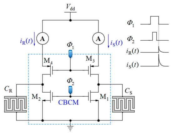
Figure 2.
Core of the charge-based capacitance measurement (CBCM).
To the best of our knowledge, all of the previously reported core-CBCM capacitive sensors integrate the whole exponential output current of the core-CBCM circuit by an integrating capacitor, and then convert the integrating capacitor voltage to digital or frequency. Conversion of the whole exponential current to voltage and working in voltage mode limit the IDR of the capacitive sensor. This IDR problem becomes more serious for CMOS technologies with lower supply voltages, in particular for life science applications.
In this paper, we focus on a new design to enhance the IDR of sensor using a current-mode method. In order to achieve higher than 10 fF IDR for cell analysis, current-mode techniques by using internal CMOS capacitors help to precisely follow the intrinsic sharp variations of the currents of core-CBCM circuits, in order to digitize and integrate them. In contrast to previous works [12,61,62,63,64,65] that average the whole CBCM current in the analog domain, the presented core-CBCM capacitive sensor does the required averaging in two steps, in both the analog and the digital domain. In this technique, a current-controlled oscillator (CCO) is used to frequency modulate the sharp exponential current of the CBCM circuit, and an adapted counter completes the integration in the digital domain. We believe our proposed solution advances previous core-CBCM methods by increasing its IDR. Additionally, in comparison to previous core-CBCM capacitance-to-frequency converters [66,67], digitization of the exponential CBCM current to very small units, and piecewise integration of this current helps to achieve a better resolution, and it is no longer necessary to use very large integrating capacitors to obtain high accuracy. Furthermore, digital outputs of capacitive sensors make reading them much easier, especially if they need to be able to connect to a microcontroller. Since the low-cost microcontrollers do not have internal ADCs, only digital [12,48,49] or semi-digital signals such as frequency modulated ones [23,67] are suitable as their inputs.
The output pulses of the proposed core-CBCM capacitance-to-frequency converter have high frequencies, and they can be destroyed by the capacitance loading effects of the output pads. Thus, a Fibonacci reverse/forward linear feedback shift register (LFSR) is adapted as an on-chip up/down counter and a serial-in–serial-out register to count and register the number of pulses and also calibrate the offset current.
In the remainder of this paper, Section 2 explains the basic principle of the CBCM method and gives a brief overview of related works on CMOS core-CBCM capacitive sensors. A new topology is proposed in Section 3. Additionally, an adapted Fibonacci reverse/forward LFSR is presented in this section. The related controlling clock strategies to meet the requirements of the sensor are described in Section 4. The simulation results will be demonstrated in Section 5, followed by a discussion in Section 6. Our conclusions are drawn in Section 7.
2. Related Works
Core-CBCM capacitive sensors have been widely used for several LoC applications such as cell viability and proliferation monitoring [12,64], bio-particle sensing [68], organic solvent monitoring [17] and DNA detection [69]. As aforementioned, this method, by offering high accuracy and low complexity, has drawn considerable attention for high throughput screening in array structures.
2.1. Principle of Core-CBCM Method
The CBCM method was originally proposed for measurement of the crosstalk capacitances in between the conductors in deep CMOS chip [70,71]. A combination of this method with other circuitries was proposed for the detection of capacitive changes in the proximity of electrodes created on the topmost metal layer [58,59,60]. The basic core of the CBCM method is depicted in Figure 2. It is composed of a sensing (CS) and a reference capacitor (CR) that can be charged or discharged via two pairs of N-Channel CMOS (NMOS) (M1 and M2) and P-Channel CMOS (PMOS) (M3 and M4) switches controlled by clock pulses Φ2 and Φ1. These two clock pulses should be non-overlapped to avoid a short-circuit current.
When Φ1 and Φ2 are both low, the capacitors CS and CR are charged via M3 and M4. When these pulses became high, the capacitors are discharged via M1 and M2. The instantaneous current of each branch, iS(t) and iR(t), can be obtained by:
where vS(t) and vR(t) are the instantaneous voltages across CS and CR, respectively. The average of iS(t) and iR(t) over one period of Φ1 and Φ2 are obtained as follows:
where IS and IR are the average of currents iS(t) and iR(t), respectively. TS denotes the period of Φ1 and Φ2 and VAm identifies the drop voltage over the ammeters. The average currents of two branches of this circuit, IS and IR, are proportional to the related capacitances. Thus, the subtraction of CS and CR (ΔC = CS − CR) can be obtained by the subtraction of these two averaged currents:
In this way, ΔC can be extracted from CS with a high accuracy. As a result, this method is suitable for LoC applications in which the sensing capacitances are very small.
2.2. Single-Ended Core-CBCM Methods
To date, many efforts have been made to leverage the advantages of the CBCM method for life science applications [12,60,62] by proposing efficient circuit topologies. In these topologies, a sharp exponential current generated in the CBCM structure should be converted into digital structure. These topologies are designed to offer fast response, high sensitivity, high linearity, and high signal-to-noise ratios (SNRs) by reducing the external noises and parasitic capacitors. Evans et al. [61] made an attempt to develop the CBCM method by presenting an on-chip readout circuit, as shown in Figure 3. In this circuit, the currents iS and iR are separately averaged by two integrating capacitors, and then the resultant voltages are fed to a differential amplifier where those voltages are amplified and subtracted. In this approach, to achieve a higher sensitivity, high voltages across integrating capacitors are required. However, this situation pushes the differential amplifier to a nonlinear region and thus limits the resolution and the IDR of the sensor. In another effort, Stagni et al. [69] utilized the CBCM method for DNA recognition using off-chip readout circuitry.
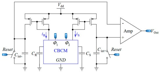
Figure 3.
A core-CBCM capacitance-to-voltage converter (CVC) that integrates the currents iS and iR before subtraction (adapted from [61]).
The first step toward a fully integrated core-CBCM capacitive sensor was taken by Ghafar-Zadeh et al. [58] by proposing a new single-ended CVC circuit that was interconnected to microelectrodes. In this sensor, the microelectrodes were implemented on the topmost layer of a CMOS technology and used as sensing electrodes for LoC applications. To mitigate the IDR problem of the approach used by Evans et al. [61], Ghafar-Zadeh et al. [58] proposed a new circuit to subtract the currents iS and iR before injection to the integrating capacitor, as shown in Figure 4. In the first block of Figure 4, the currents of CBCM block, iS and iR, are mirrored, amplified, and then subtracted by using the current mirrors realized by M5-10. It is straightforward to verify that the instantaneous current iX(t, CS, CR) in Figure 4 is equal to Equation (6):
where K1, K2 and K3 stand for the gain of the first (M5,7), the second (M6,8), and the third (M10,9) current mirrors, respectively. To achieve a symmetric structure, it is better to choose K3 = 1 and K1 = K2. If K1 = K2 = K, the integration of iX during one period of Φ1 and Φ2 can be expressed as follows:
where Vdd is the power supply voltage and Vthp is the PMOS threshold voltage. Sensing and reference capacitors are charged to nearly Vdd-Vthp during the charging interval. Averaging over N cycles of Φ1 and Φ2, we can improve the sensitivity of the sensor. Let us assume that the total integration time is Tint = NTS, and we obtain the integration of iX during this interval as follows:
which is proportional to ΔC. In [58], the current iX is integrated in the analog domain by the second block shown in Figure 4 using an integrating capacitor. As the continuation of that work, a single-ended sigma delta (ΣΔ) modulator was designed for converting the analog voltage to digital data [17]. Contrary to conventional ADCs, the input analog voltage of this ΣΔ modulator is a step signal instead of a ramp. In other efforts, they showed the ability of their proposed circuit to monitor the organic solvent and bacteria growth [62,72]. In [73], the CBCM technique is used in a 256 × 256 array for high impedance spectroscopy and imaging where the CBCM currents are integrated by integrating capacitors, and the output voltages are digitized by eight ADCs.
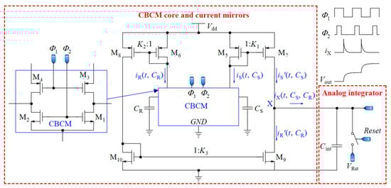
Figure 4.
A core-CBCM CVC that subtracts the currents iS and iR before integration (adapted from [58]).
2.3. Fully Differential Core-CBCM Capacitive Sensor Method
As the continuation of the work discussed in the last Section 2.2, a fully differential core-CBCM CVC was proposed by Prakash et al. in order to double the IDR and to mitigate the effect of common mode noise and the parasitic capacitances of these single-ended core-CBCM capacitive sensors, for cell-sensing applications [60,64] (Figure 5). In [74], cascade current mirrors were used in the same structure to improve the output impedance of current mirrors and to achieve better results for impedance measurement. In another effort, a fully differential core-CBCM capacitance-to-digital converter was reported in [65] by using an adapted fully differential sigma delta (ΣΔ) modulator. This modulator can be used to convert the capacitance to digital in an array of core-CBCM capacitive sensor [12]. Although the integration of the currents iS and iR after subtraction in both single-ended [17,58,62,72] and fully differential architectures [12,60,64,65] shows wider IDRs in comparison to the approach depicted in Figure 3 [61], averaging the whole amplified differential current of the CBCM core by integrating capacitors still limits the IDR.
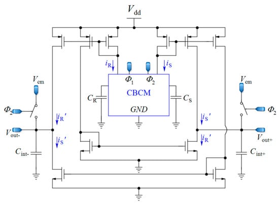
Figure 5.
Fully differential core-CBCM CVC adapted from [60,64].
2.4. Core-CBCM Capacitance-to-Frequency Converter
In [66], a capacitive sensor is proposed, utilizing a combination of CBCM method and capacitance-to-frequency conversion, as illustrated in Figure 6. In this circuit, the sharp exponential currents of each branch of the CBCM block are averaged using a large integrating capacitor (Cint) in the analog domain, and then this voltage is converted to frequency by a comparator. Two similar structures are used for each of the sensing and reference capacitors in order to convert the related capacitance to frequency. The subtraction of the output frequencies of the two branches is proportional to ΔC. In this circuit, the whole integration of the CBCM exponential current is performed in the analog domain, as with the previous circuits and then the resultant voltage is converted to frequency. This circuit requires a very large integrating capacitor to achieve a proper charging time difference, and it works from a femto-Farad to pico-Farad range, which is not suitable for LoC applications. Yamane et al. [67] used a similar approach by an integrator and a Schmitt trigger. However, it also suffers from low resolution.
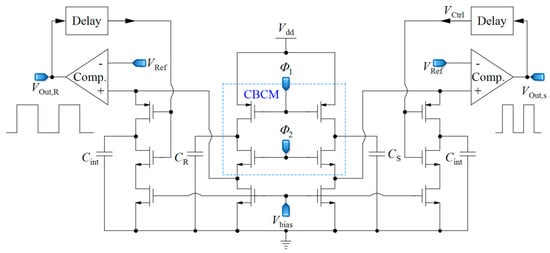
Figure 6.
A core-CBCM capacitance-to-frequency converter that integrates all of the exponential CBCM currents in the analog domain and converts them to two frequencies (adapted from [66]).
In sum, all aforementioned core-CBCM capacitive sensors reported in the literature work in a voltage mode and integrate the whole exponential CBCM current in the analog domain using integrating capacitors that convert the current to voltage. As a result, the IDR of the sensing capacitance is limited by the voltage swing of the integrating capacitor. Current-mode circuits are more suitable for low supply voltage CMOS technologies. Thus, this paper proposes a novel core-CBCM capacitance-to-frequency converter working in current-mode in order to increase IDR. Utilizing the internal capacitors of CMOS transistors makes it possible to follow the sharp variations of CBCM currents and to use both the analog and the digital domains to integrate CBCM currents.
3. Proposed Core-CBCM Capacitive Sensor
In the proposed capacitive sensor shown in Figure 7, the currents of the two branches of the CBCM core are amplified and subtracted using the current mirrors and then fed into a CCO. The CCO should be able to follow the variations of the sharp exponential currents of the CBCM block, so that it modulates them to pulse frequency. Since the average of the differential current is proportional to ΔC, a counter is used to average the output frequency. In other words, unlike previous works, in the presented sensor, the required averaging operation is not done only in the analog domain. More detailed descriptions of the proposed capacitive sensor are presented in the following subsections.
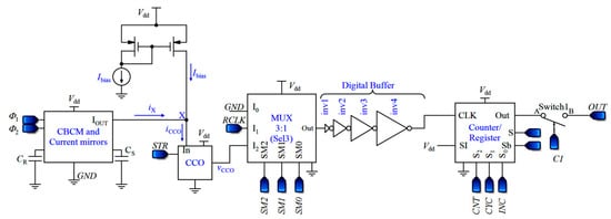
Figure 7.
Block diagram of the proposed capacitive sensor.
3.1. Description of the Sensor Performance
Prior to describing the sensor performance let us calculate the integration of the input current of the CCO block over a specific time. Thereafter, two approaches are put forward to achieve a practical result that is proportional to ΔC.
3.1.1. Core-CBCM Block Performance and the Bias Current
The analog circuit of the first block of Figure 7 is the first block of the circuit illustrated in Figure 4, including the CBCM core and current mirrors (without the analog integrator). A direct current, Ibias, is also added to iX to shift the CCO operating area to its linear region (iCCO = iX + Ibias). Assuming Tint = NTS, we can obtain the integration of iCCO during this interval as follows:
which changes with ΔC linearly.
3.1.2. The First Description of the Sensor Performance
The basic design of a CCO from [75] is illustrated in Figure 8a. In this circuit, the nodes V1 and V2 are alternatively charged by the input current of the CCO (iCCO), and they produce the output voltages V3 and V4. Because of the latch, V3 and V4 are the inversions of each other. The frequency of the output nodes depends on the time that is required for V1 and V2 to reach a toggling voltage (Vtog) in order to change the state of the latch. Thus, the integration of iCCO in the required interval (Tm) for V1 (or V2) to reach Vtog is obtained as follows:
where C1 is the total capacitance seen at nodes V1 or V2 (for a symmetrical CCO circuit). C1 consists of the junction capacitances of the transistors, and is very small. So, a little change in iCCO results in a significant variation in the CCO output frequency. As C1Vtog is almost constant, the larger amplitude of iCCO leads to shorter interval (Tm) and vice versa. Thus, as shown in Figure 8b, the total area under iCCO(t) during a specified time can be divided into very small blocks with an area of C1Vtog for each one (Here we call them unit blocks). For example, J unit blocks with the area of C1Vtog can be obtained during TS (Figure 8b–d shows this concept by exaggeration in the sizes of the unit blocks). After each Tm (m = 1, 2,…, J), the state of the output voltage of the CCO (vCCO) changes from low to high or conversely high to low (Figure 8c). The integration of iCCO during Tint is equal to Equation (11):
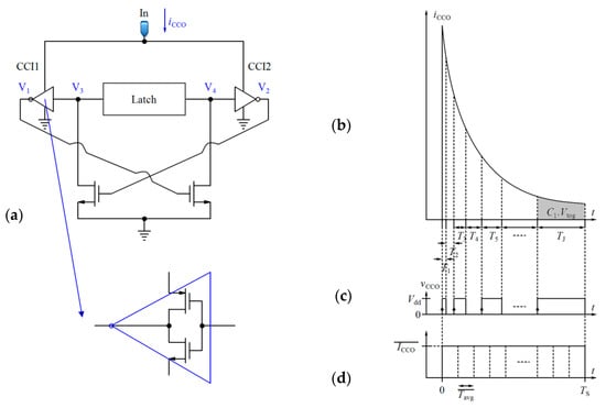
Figure 8.
(a) Basic design of the CCO [75], (b) CCO input current, (c) CCO output voltage, (d) CCO averaged input current based on the mean value theorem.
A counter can be used to count these blocks. In this way, the integration process will be completed in the digital domain. If the counter counts only the rising edges of the pulses, the number counted by the counter (Numb) during Tint will be equal to NJ/2. It is easy to verify that using Equation (12):
where N is an even number. Assuming Vtog is constant, the relation between Numb and ΔC will be linear.
3.1.3. The Second Description of the Sensor Performance
One may argue that the sharp exponential input current of the CCO is a frequency modulated current. Although the CCO does not convert its input current to frequency in every moment of the integration time, its output frequency follows the envelope of the discrete variable frequency of the output pulses (see Figure 9 as an exaggerated illustration). In an ideal case, the output frequency of the CCO is given by Equation (13):
where M denotes the gain of the CCO. Combining Equations (6) and (13) and averaging the result over one period of Φ1 and Φ2, we deduce the following equation:
where FCCO identifies the average of the variable frequencies of the output pulses over TS and Vthp is the threshold voltage of the PMOS transistors. For the total averaging time (Tint), it can be simply shown that:
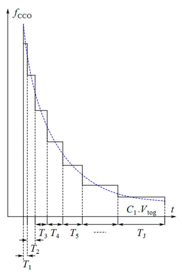
Figure 9.
Frequency of the output pulses of the CCO and its envelope (by exaggeration in the sizes of the unit blocks).
As seen from Figure 8c, a half period of each pulse is produced for each unit block. We can therefore use the mean value theorem to obtain Equation (16):
which is equal to the counter number (Numb). Thus, the sensitivity of the sensor can be obtained by Equation (17):
Equation (17) shows that there are three parameters affecting the sensitivity of the sensor including the gain of the current mirrors used in the first block (K), the sensitivity of the CCO (M), and the number of the cycles of Φ1 and Φ2 (N), with the latter being off-chip controllable. It should be pointed out that the IDR of the CCO and the size of the counter can limit the IDR of the sensor. A trade-off should be considered for the value of K. The more gain that is dedicated to the first block, the less IDR that is achieved for the sensor. However, this results in greater sensitivity. The sensitivity can be increased by two other parameters, N and M. However, rising N brings about a longer measurement time.
In summary, the proposed circuit integrates the current signals in each period in two steps. First, the CCO integrates the current over the time required for each unit block in the analog domain. Then, the counter counts the unit blocks and completes the integration in the digital domain. Each unit block produces an individual frequency at the output of the CCO. Finally, a string of the pulses with discrete frequencies will appear at the output of the CCO that follows the envelope of the instantaneous frequency modulated current response of the core-CBCM circuit (Figure 9). The small junction capacitances of the transistors used as the integrating capacitor of the CCO make it capable of high digitization of the sharp exponential current of the core-CBCM circuit. On the other hand, the current-mode operation of the CCO helps to overcome the IDR limitation that is imposed by the supply voltage.
3.2. Current-Controlled Oscillator (CCO)
3.2.1. Performance of the Used CCO
Since the waveform of the current iCCO(t) is very sharp, the CCO should be able to follow the fast variations in iCCO(t). Here, the CCO proposed in [75] was selected because of its striking features, such as wide IDR and very low sensitivity to power supply voltage variations (Figure 10).
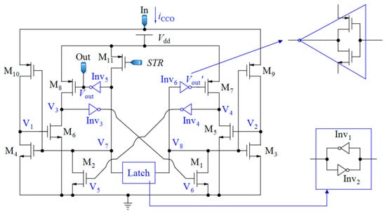
Figure 10.
Complete current-controlled oscillator proposed in [75].
For the performance description of this CCO, we can start from node V7. If the voltage of this node (V7) is high, M10 is turned off; while M4 is turned on, discharges the voltage at node V1 to zero. At the same time, the voltage of V8 is low and M3 is in the cut-off region. Additionally, M9 is in the saturation region and steers the input current iCCO to charge the total capacitance that is seen at node V2. When the rising voltage of V2 reaches the threshold voltage of M5, this transistor is turned on and pulls down the voltage at node V4. When this voltage is about half of the supply voltage (Vdd/2), through Inv4, M2 is turned on and it changes the state of the latch that is composed of the two inverters, Inv1 and Inv2. In the new state, the input current iCCO charges the total capacitance at node V1, and the voltage of V2 becomes zero. An alternative performance of this process brings about the output pulses whose frequencies are proportional to the input current of CCO (iCCO). It can be proven that the relation between the frequency of the output pulses and the input current is obtained by Equation (18) [75]:
where I0 stands for a technology-dependent scaling parameter, VT denotes the thermal voltage, and n identifies the subthreshold gate coupling coefficient. C1 and C3 are the total capacitances that are seen at nodes V1 and V3, respectively. Vthn is the NMOS threshold voltage, W6 denotes the channel width, and L6 is the channel length of M6. Both transistors M5 and M6, have the same sizes because of symmetry, and they operate in the sub-threshold region. According to Equation (18), and knowing that C1 is a very small capacitor; the output frequency is proportional to iCCO. The large sizes of M5 and M6 help to reduce the effects of variations in the process parameters and the mismatches on the capacitor C3, but at the expense of less sensitivity of the CCO. Thus, a trade-off should be considered to achieve a suitable linearity and sensitivity. The transistor M11 is used to start-up the oscillation controlled by signal STR. When STR is low, the voltage at node V7 rises up toward Vdd, and after commencing the oscillation of CCO, M11 is turned off.
3.2.2. Effect of the Nonlinearity of the CCO on the Sensor Response
Since the toggling voltage at nodes V1 or V2 (Vtog) of the circuit shown in Figure 10 is dependent on the input current iCCO, the CCO has a nonlinear behavior. Equation (18) reveals that the logarithmic term in the denominator is the main reason for this nonlinearity. Although this CCO is designed for a direct current in [75], it can be proven that it is also useful for our time-varying current. Based on the mean value theorem, the area under the graphs of the signals shown in Figure 8b,d are the same. In Figure 8d, and . Thus, it is straightforward to verify that:
Since the number of rising edges during Tint is equal to NJ/2, the relation between this number (Numb) and ΔC can be calculated by:
Using the approximations of and for , we can find a straightforward relation, as shown in Equation (21):
If, the values of , , and can be obtained as follows:
where F >> 1 and . Thus, there is second-order nonlinearity in the final response of the capacitive sensor which is reduced by increasing Ibias.
3.3. Counter and Register
The employed counter should be fast enough to follow the pulses with variable frequencies. The Fibonacci linear feedback shift register (LFSR) is chosen due to its high speed, low circuit complexity, and thus its small area. Furthermore, it can be utilized as both a counter and a serial-input serial-output register.
The presence of bio-particles or other remnants in the micro-channels and the non-idealities of the circuit such as parasitic capacitances, mismatches in the current mirrors, the effects of temperature variations cause an offset current for ΔC = 0. Furthermore, the bias current, Ibias, and its non-idealities are added to the offset current. This offset current might saturate the system. Thus, there should be enough of a secure margin between the IDR of the CCO and the maximum mirrored current of the core-CBCM circuit. Here, the circuit is calibrated by designing an LFSR-based up/down counter. When the sensing electrode is not exposed to the biochemical sample (ΔC = 0), the shift register shifts the data reversely. Then, the resultant value is registered as the initial value of LFSR for up-counting. After applying the sample to the sensing electrode, the counter commences forward shifting of the registered initial data. In other words, this approach helps to omit the large term of from Equation (21), and thus, it results in higher measurement accuracy.
The 16-bit counter used in the proposed sensor is a combined and adapted version of the bidirectional LFSR proposed in [76], and the LFSR-based counter used in [77]. The feedback polynomials of LFSR for forward counting are known. In order to find feedback polynomials for reverse counting, the Karnaugh map can be used. Since using a Karnaugh map for 16 bits is overwhelming, we will start with smaller sizes of LFSRs. As seen in Table 1, there is a repetitive relation between the structures of the reverse and forward LFSRs with the same sizes. Thus, it is possible to guess the feedback polynomial for a reverse LFSR, based on the polynomial for forward counting. The feedback polynomial for a 16-bit forward LFSR is x16 + x15 + x13 + x4 + 1, and based on the repetitive trend shown in Table 1, the one for reverse counting will be x16 + x14 + x5 + x1 + 1. The utilized LFSR-based reverse/forward counter/register is depicted in Figure 11.

Table 1.
Forward and reverse linear feedback shift register (LFSR) with three different sizes (the rectangles stand for D flip-flops).
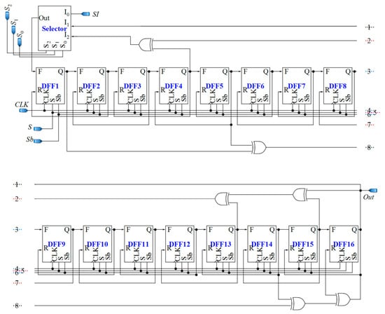
Figure 11.
Proposed 16-bit LFSR-based reverse/forward counter/register.
D flip-flops used in the up/down counter should be fast and static. This is because the output pulses of the CCO have various frequencies, and the D flip-flops should be able to follow the pulses and save their own data until the next pulse comes. Additionally, two different inputs are required for D flip-flops, one for reverse shifting, and the other one for forward shifting. Figure 12a demonstrates the D flip-flop that is used in the counter, which is composed of two blocks, a 2:1 multiplexer and the fast static D flip-flop that is presented in [79]. The controlling signal Sb of the multiplexer is the inverted version of S. By using the multiplexer, the required input is selected and fed to the D flip-flop. F and R inputs are for forward and reverse counting, respectively. Moreover, the XOR gates used in the counter should be fast enough. Figure 12b shows the XOR gate proposed in [78], operating based on a differential cascade voltage switch with a pass-gate (DCVSPG). The multiplexers used in the sensor and their controlling signals make the sensor operate in five different phases, which is described in the next section. Also, a digital buffer is placed between the CCO and the counter to avoid changing the frequencies of the output pulses of the CCO due to the counter-loading effect (Figure 7).
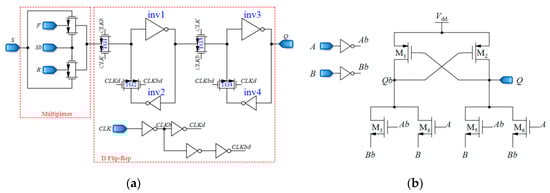
Figure 12.
(a) Fast static D flip-flop, (b) Fast XOR gates based on a differential cascade voltage switch with a pass-gate (DCVSPG) [78].
3.4. Interdigitated Microelectrodes
Sensing and reference capacitors are co-planar interdigitated electrodes that are fabricated by the topmost layer of CMOS technology. The parasitic capacitors of the electrodes are depicted in Figure 13. Each electrode consists of two parts, E1 and E2. CR1, CR2, and C12 are the parasitic capacitances between E1 and the substrate, between E2 and the substrate, and between E1 and E2, respectively. Since one side of the electrode, E2, is grounded, the total capacitance seen at the node of the reference electrode is equal to the parallel combination of CR1 and C12. For the sensing electrode, the corresponding capacitance of the aqueous sample which is applied to the electrode should be added to CR.
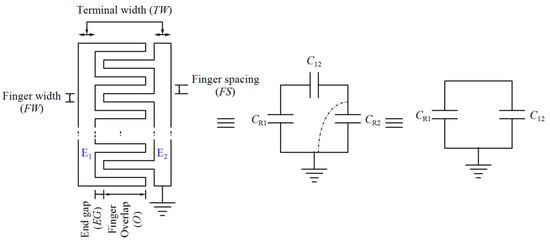
Figure 13.
Model of interdigitated electrodes.
4. Clocking Strategy of the Sensor
The proposed sensor works in five phases. The waveforms of the sensor signals and the controlling signals corresponding to each phase are depicted in Figure 14 and Table 2. These phases are explained as follows.
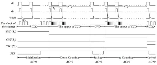
Figure 14.
Different waveforms of the proposed sensor.
Table 2.
Five phases of the sensor and the related situations of the controlling signal.
Initialization: Before employing the biochemical sample to the electrodes, by rising the signal INC, which is connected to the selecting pin S0 of the counter (as shown in Figure 7 and Figure 11), all D flip-flops receive the input SI, which is connected to the supply voltage. In this phase, D flip-flops work with an optional low frequency clock pulse (RCLK) with a period of TC. After 16TC, all D flip-flops are ready to start counting.
Down counting for ΔC = 0: In this phase, the sensing capacitor, CS, is free of biochemical sample. The output of the CCO, which has already started its oscillation, is fed to D flip-flops as their clock pulses. Simultaneously, the counter is set to count reversely. The counter should shift the data in the reverse direction over an interval that is equal to Tint=NTS. In this situation, the signal Sb of D flip-flops is high, and all three signals CYC, INC, and CNT are low. Thus, the D flip-flops receive the data on their R input.
Saving mode (ΔC = 0): In this phase, the sensing capacitor is not yet exposed to the biochemical sample. However, the controlling signal, SM0, is high. Thus, the D flip-flops of the counter receive no pulses and they act as registers.
Up-counting (ΔC ≠ 0): In this phase, the biochemical sample is applied to the sensing capacitor and the counter is adjusted for forward counting of the output pulses of the CCO. The controlling signals INC and CYC are low, and the signal CNT is high for an interval equal to Tint.
Cycling: The number of the counted pulses during Tint goes out serially at a particular frequency (1/TC). Thus, RCLK is fed to D flip-flops again, which has a low frequency equal to fC = 1/TC. The low frequency of RCLK mitigates the capacitance loading effect of the output pin.
5. Results
The proposed sensor is simulated in a 0.18 μm CMOS technology. The post-layout simulation results are shown in this section. The CCO is the core of the sensor that should be capable of following the demonstrated and discussed specifications.
5.1. Linear Region of the CCO
Figure 15a shows the response of the CCO separately, which is examined by applying a DC input current to the CCO, and the measurement of the frequency of its output pulses. The nonlinearity error for lower input currents is higher, as seen in Figure 15b. The added bias current Ibias shifts the operating area of the CCO to the more linear region, and thus, helps to have a CCO with more linear behavior. This is equivalent to decrease in Equation (21) for the whole sensor.
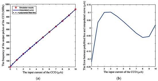
Figure 15.
(a) CCO output frequency vs DC input current, (b) Error between the polynomial fitted line and the simulation results.
5.2. The Response of the Analog Part of the Sensor
Figure 16a–c shows the transient response of the proposed sensor for a specific ΔC (60 fF). The input current, the output frequency (fCCO), and the output voltage of the CCO (vCCO) are illustrated in Figure 16a–c, respectively. Since the frequencies of the output pulses of the CCO are so high, the pulses are so compact that they cannot be distinctly illustrated for just one period of Φ1,2 (TS). Thus, in Figure 16, the bias current is omitted (iCCO = iX) to lower the frequency level of output pulses, and to show the concept of the proposed solution more clearly. Based on the waveforms shown in Figure 16, the CCO has enough speed for following the sharp exponential currents of the core-CBCM circuit. It is worthwhile noting that the jitter of the CCO does not affect the sensor response significantly. This is because the integration time (Tint = NTS) is long enough so that the jitter averages out at zero.
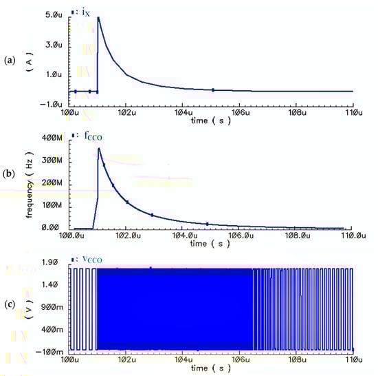
Figure 16.
(a) Variations of the CBCM output current (iX) versus time, (b) Variations of the output frequency of the CCO (fCCO) versus time, (c) Variations of the CCO output voltage pulses (vCCO) for the CBCM output current as the CCO input (iCCO = iX) for ΔC = 60 fF (in order to show the compact high frequency pulses more clearly and to lower their frequencies, Ibias is omitted from the input of the CCO).
The input current of the CCO, considering the required bias current (iCCO = iX + Ibias) and the output frequency of the CCO are depicted for five different ΔCs versus time in Figure 17a,b, respectively.
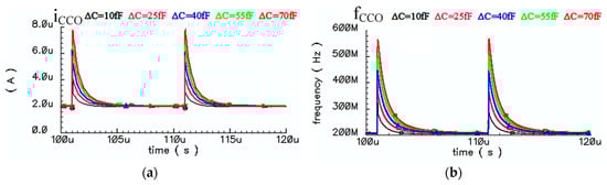
Figure 17.
(a) Input current of the CCO, (b) CCO output frequency versus five different ΔCs.
Figure 18a,b shows the integration of iCCO and fCCO over the total integration time (Tint) versus different ΔCs. Based on Figure 18, the first block, including the CBCM core, and also the bias current mirror, show a linear response with respect to the variations of ΔC. As shown in Figure 16b, and expected from Equation (15), the integration of fCCO over Tint has an almost linear variation versus ΔC. Based on the descriptions explained for the sensor performance, it is also expected to obtain a linear response from the practical circuit, in which the counter completes the integration operation in the digital domain.
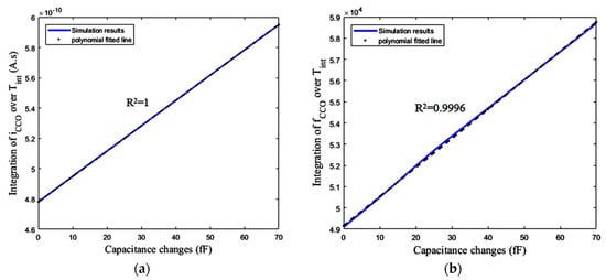
Figure 18.
(a) Integration of iCCO over Tint versus ΔCs, (b) Integration of fCCO over Tint versus ΔCs.
5.3. The Response of the Whole Practical Sensor, Its Nonlinearity, and Its Temperature Dependency
Based on Figure 17b, the maximum output frequency of the CCO for ΔC = 70 fF is less than 600 MHz. The counter is designed for clock pulses with a frequency that is more than this value (about 1 GHz). Using the LFSR structure and the reduced setup time D flip-flop proposed in [79] in the adapted LFSR helps to meet this requirement
Figure 19a demonstrates the number of pulses that are counted by the counter, versus the changes of the sensing capacitance up to 70 fF. Assuming that the temperature is not changed after calibration, this simulation, along with the associated calibration, is repeated at three different temperatures of 15 °C, 27 °C, and 45 °C. The slope of the polynomial fitted line represents the sensitivity of the sensor, which is about 138 pulses/fF at room temperature (27 °C). Ideally, for a completely linear response, this sensitivity should have a resolution of about 7.2 aF. However, the response is not completely linear.
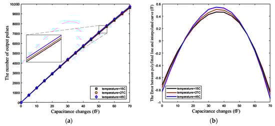
Figure 19.
(a) Number of pulses versus capacitance changes ΔC (fF), (b) Error between the simulation results for 15 different values of ΔC and the polynomial fitted line (at three different temperatures of 15 °C, 27 °C and 45 °C).
One method for the measurement of this nonlinearity is R-squared (R2). It is a statistical measure showing how close our response data are to the fitted straight regression line. Based on this method the linearity of the response shown in Figure 19a is approximately R2 = 0.9996, meaning that 99.96% of the counter number variations can be explained by a linear model for capacitance changes (ΔC) of up to 70 fF. Figure 19b shows the error between the simulated curve obtained from the circuit simulator and the polynomial fitted line (using linear least squares) with this curve for the mentioned range of ΔC. Based on this figure, the maximum absolute error due to the nonlinearity of the circuit is about 873 aF, which limits the resolution of the sensor. This nonlinearity also exists in Figure 18b with the same value of R-squared, while Figure 18a has an R-squared value equal to one. This means that the first block, including CBCM core has a good linearity. Thus, the original source of this nonlinearity is the nonlinearity of the CCO, which is predictable by Equations (20) to (24).
In Figure 19a, a higher temperature results in a slight increase in the slope of the fitted line. As shown in Figure 19a,b, the sensor has a negligible temperature dependency.
By using intentional pre-distortion, it is possible to achieve better resolution. First of all, the number of output pulses is measured for different values of ΔC from zero to 70 fF at 5 fF steps, and a look-up table is formed for these 15 points. This can be done with a capacitor bank. The interpolation of these points gives us an estimation of the trend of the curve for other values of ΔC. Thereafter, the interpolated curve can be utilized for pre-distortion in order to reduce the effect of the nonlinearity. Figure 20a shows the number of output pulses for 15 values of known ΔCs in 5 fF steps. Additionally, the polynomial-fitted line and the interpolated curve are depicted in this figure. For any other measured number of pulses, the nearest point of the interpolated curve to the measured value is selected. Based on the interpolated curve, the corresponding ΔC can be estimated. As illustrated in Figure 20b, if the difference between the interpolated curve and the polynomial fitted line for the related ΔC is subtracted from the measured numbers of pulses, the value of corresponding ΔC is estimated by the pre-distorted point and the fitted line with an error less than 10 aF. In other words, interpolation and pre-distortion techniques provide a resolution of about 10 aF for ΔC.
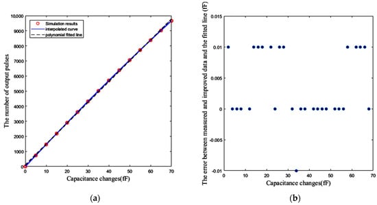
Figure 20.
(a) Fifteen measured number of pulses versus capacitance changes ΔC (fF) at 27 °C, and the interpolated curve and the polynomial fitted line to these 15 points. (b) The error between the measured numbers of pulses related to the other values of ΔC after pre-distortion, and the polynomial fitted line.
5.4. Mismatch Effects
The effects of mismatch errors are depicted in Figure 21. A total of 20% of changes in the width of the transistors M6 and M5 of the CCO (see Figure 10) and M8 and M7 of the current mirrors (see Figure 4) affect the sensitivity of the CCO and the aspect ratio of the current mirrors, respectively, which both change the sensitivity of the sensor. Mismatch errors cause some offsets in the response of the sensor that can be omitted by the down-counting approach. However, the mismatch of M7 of the current mirrors results in a more destructive impact on the response of the sensor, because it changes the aspect ratio K1 in Equation (6), leading to both the slope and offset variations of the response with respect to ΔC. Thus, in spite of the elimination of the offset by the counter, we need a two-point calibration to correct the slope variations, due to mismatch.
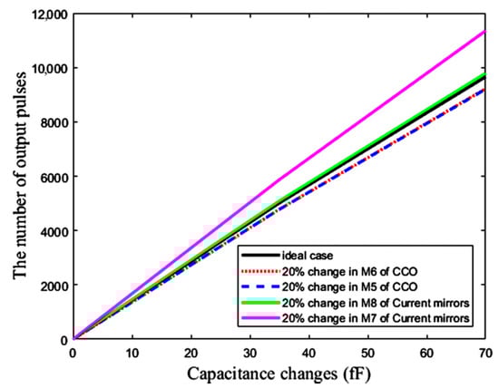
Figure 21.
The effect of mismatch error on the capacitive sensor output after the elimination of offset.
5.5. Other Specifications of the Sensor
Figure 22 shows the layout of the proposed capacitive sensor, along with the reference and sensing interdigitated electrodes. The total area occupied by the interface circuit is 24 μm × 300.98 μm, and the total area of one cell of this capacitive sensor is 214.275 μm × 300.98 μm. The interdigitated electrodes are simulated in Sonnet software to estimate the value of reference capacitor and the effect of the cell confluency percentage on the value of the sensing capacitor (CS). The number of fingers, the spaces between the fingers and the fingers overlaps of the electrodes are 15, 5 μm, and 60 μm, respectively. Thus, the area of one interdigitated electrode is 80 μm × 295 μm, which can be changed based on the application and the accessible chip area. Here, fibroblast cells with an electrical conductivity of 5 S/m and a relative permittivity equal to 1 are used to examine this concept. Figure 23 illustrates the roughly linear upward trend of the value of CS for increasing the cell confluency percentage. The characteristics of the proposed sensor are summarized in Table 3. The powers of the two first blocks, including the CBCM core and the CCO, are dynamic, which are reported for 35 fF and a sampling frequency of 100 kHz, in Table 3.
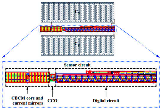
Figure 22.
Layout of the proposed capacitive sensor, along with sensing and reference electrodes.
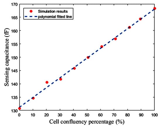
Figure 23.
Sensing capacitance versus fibroblast cell confluency percentage.
Table 3.
Core-CBCM capacitance-to-frequency converter specifications.
6. Further Discussions and Future Works
The characteristics of the simulated circuit are compared with the other core-CBCM capacitive sensors in Table 4. The simulation results of the proposed circuit indicate that it has a considerably wider IDR, in comparison to the previous works. Here, the IDR and the nonlinearity of the CCO and the size of the counter are the limiting factors for the IDR of ΔC. However, working in current-mode assists with having an appropriate IDR. Moreover, the sensitivity of the sensor can be off-chip-controllable, and it tends to vary by the cycles (N) of the integration time (Tint = NTS): the more quantitative the cycles, the greater the achievable sensitivity.
Table 4.
Comparison of CMOS capacitive biosensors.
To sum up, the results suggest that the proposed capacitive sensor can be a candidate form of architecture for LoC applications such as cellular monitoring. Systematically speaking, the platforms used in these applications require microfluidics to manipulate, control, and steer the aquatic sample towards the electrodes of the biosensor. Packaging microfluidics and CMOS biosensors, and their biocompatibilities are some important issues in these applications. The fabrication of this capacitive sensor, along with microfluidics and a suitable packaging, is considered as future works. Further experiments should be conducted for the evaluation of the sensor for different life science applications. Additionally, controlling the environmental temperature can be an effective factor that should be considered. Furthermore, an array of the sensor-like structure that is shown in Figure 24 makes it possible to perform measurements for different samples simultaneously and paves the way for high-throughput screening. Since the proposed capacitor can register the data, different measurements can be done simultaneously. Then, the registered data can be selected and read by a multiplexer.
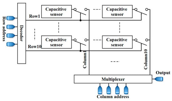
Figure 24.
A 10 × 10 array of the proposed capacitive sensor.
7. Conclusions
Previously reported core-CBCM circuits operate based on a current-to voltage-integrator. This paper presents a new core-CBCM capacitive sensor with a wide input dynamic range using a current-mode method, and internal capacitors of CMOS transistors. This new design consists of a high-speed current-controlled oscillator and a fast counter, in order to convert the output current of the CBCM block to variable pulse frequencies. The simulation results indicate a linear relationship between the capacitance and the sensor’s output, with an input capacitance range of around 70 fF, and an absolute error of less than 873 aF. Based on these results, the proposed core-CBCM circuit with an improved IDR and high resolution is the best candidate for the development of high throughput capacitive sensor arrays that are suitable for life science applications.
Author Contributions
This work, including the design, simulation, and implementation of the CMOS chip, and the preparation of the first draft of paper, was prepared by S.F. under the co-supervisions of E.G.-Z. and R.D.
Funding
This research received no external funding.
Acknowledgments
Authors thanks the technical support of Canadian Microsystem Corporation (CMC).
Conflicts of Interest
The authors declare no conflict of interest.
References
- Kar, S.K.; Chatterjee, P.; Mukherjee, B.; Swamy, K.B.M.M.; Sen, S. A differential output interfacing ASIC for integrated capacitive sensors. IEEE Trans. Instrum. Meas. 2018, 67, 196–203. [Google Scholar] [CrossRef]
- Utz, A.; Walk, C.; Stanitzki, A.; Mokhtari, M.; Kraft, M.; Kokozinski, R. A high precision MEMS based capacitive accelerometer for seismic measurements. In Proceedings of the 2017 IEEE SENSORS, Glasgow, UK, 29 October–1 November 2017. [Google Scholar]
- Walker, G. A review of technologies for sensing contact location on the surface of a display. J. Soc. Inf. Disp. 2012, 20, 413–440. [Google Scholar] [CrossRef]
- Pedrocchi, A.; Hoen, S.; Ferrigno, G.; Pedotti, A. Perspectives on MEMS in bioengineering: A novel capacitive position microsensor [and laser surgery and drug delivery applications]. IEEE Trans. Biomed. Eng. 2000, 47, 8–11. [Google Scholar] [CrossRef] [PubMed]
- Kou, H.; Zhang, L.; Tan, Q.; Liu, G.; Lv, W.; Lu, F.; Dong, H.; Xiong, J. Wireless flexible pressure sensor based on micro-patterned graphene/pdms composite. Sens. Actuators A 2018, 277, 150–156. [Google Scholar] [CrossRef]
- Deng, W.-J.; Wang, L.-F.; Dong, L.; Huang, Q.-A. LC wireless sensitive pressure sensors with microstructured PDMS dielectric layers for wound monitoring. IEEE Sens. J. 2018, 18, 4886–4892. [Google Scholar] [CrossRef]
- Chattopadhyay, M.; Chowdhury, D. A new scheme for reducing breathing trouble through MEMS based capacitive pressure sensor. Microsyst. Technol. 2016, 22, 2731–2736. [Google Scholar] [CrossRef]
- Asano, S.; Muroyama, M.; Bartley, T.; Kojima, T.; Nakayama, T.; Yamaguchi, U.; Yamada, H.; Nonomura, Y.; Hata, Y.; Funabashi, H. Surface-mountable capacitive tactile sensors with flipped CMOS-diaphragm on a flexible and stretchable bus line. Sens. Actuators A 2016, 240, 167–176. [Google Scholar] [CrossRef]
- Pichorim, S.F.; Gomes, N.J.; Batchelor, J.C. Two solutions of soil moisture sensing with RFID for landslide monitoring. Sensors 2018, 18, 452. [Google Scholar] [CrossRef] [PubMed]
- Stagni, C.; Guiducci, C.; Benini, L.; Riccò, B.; Carrara, S.; Samorí, B.; Paulus, C.; Schienle, M.; Augustyniak, M.; Thewes, R. Cmos DNA sensor array with integrated A/D conversion based on label-free capacitance measurement. IEEE J. Solid State Circuits 2006, 41, 2956–2964. [Google Scholar] [CrossRef]
- Mirsky, V.M.; Riepl, M.; Wolfbeis, O.S. Capacitive monitoring of protein immobilization and antigen–antibody reactions on monomolecular alkylthiol films on gold electrodes. Biosens. Bioelectron. 1997, 12, 977–989. [Google Scholar] [CrossRef]
- Nabovati, G.; Ghafar-Zadeh, E.; Letourneau, A.; Sawan, M. Towards high throughput cell growth screening: A new CMOS 8 × 8 biosensor array for life science applications. IEEE Trans. Biomed. Circuits Syst. 2017, 11, 380–391. [Google Scholar] [CrossRef] [PubMed]
- Prakash, S.B.; Abshire, P. On-chip capacitance sensing for cell monitoring applications. IEEE Sens. J. 2007, 7, 440–447. [Google Scholar] [CrossRef]
- Prakash, S.B.; Abshire, P. Tracking cancer cell proliferation on a CMOS capacitance sensor chip. Biosens. Bioelectron. 2008, 23, 1449–1457. [Google Scholar] [CrossRef] [PubMed]
- Romani, A.; Manaresi, N.; Marzocchi, L.; Medoro, G.; Leonardi, A.; Altomare, L.; Tartagni, M.; Guerrieri, R. Capacitive sensor array for localization of bioparticles in CMOS lab-on-a-chip. In Proceedings of the 2004 IEEE International Solid-State Circuits Conference (IEEE Cat. No.04CH37519), San Francisco, CA, USA, 15–19 February 2004. [Google Scholar]
- Jolly, P.; Batistuti, M.R.; Miodek, A.; Zhurauski, P.; Mulato, M.; Lindsay, M.A.; Estrela, P. Highly sensitive dual mode electrochemical platform for microrna detection. Sci. Rep. 2016, 6, 36719. [Google Scholar] [CrossRef] [PubMed]
- Ghafar-Zadeh, E.; Sawan, M. A core-CBCM sigma delta capacitive sensor array dedicated to lab-on-chip applications. Sens. Actuators A 2008, 144, 304–313. [Google Scholar] [CrossRef]
- Jain, V.; Hole, A.; Deshmukh, R.; Patrikar, R. Dynamic capacitive sensing of droplet parameters in a low-cost open EWOD system. Sens. Actuators A 2017, 263, 224–233. [Google Scholar] [CrossRef]
- Guler, M.T.; Bilican, I. Capacitive detection of single bacterium from drinking water with a detailed investigation of electrical flow cytometry. Sens. Actuators A 2018, 269, 454–463. [Google Scholar] [CrossRef]
- Couniot, N.; Francis, L.A.; Flandre, D. A 16 × 16 cmos capacitive biosensor array towards detection of single bacterial cell. IEEE Trans. Biomed. Circuits Syst. 2016, 10, 364–374. [Google Scholar] [CrossRef] [PubMed]
- Hagleitner, C.; Lange, D.; Hierlemann, A.; Brand, O.; Baltes, H. Cmos single-chip gas detection system comprising capacitive, calorimetric and mass-sensitive microsensors. IEEE J. Solid State Circuits 2002, 37, 1867–1878. [Google Scholar] [CrossRef]
- Qin, Y.; Gianchandani, Y.B. A fully electronic microfabricated gas chromatograph with complementary capacitive detectors for indoor pollutants. Microsyst. Nanoeng. 2016, 2, 15049. [Google Scholar] [CrossRef]
- Senevirathna, B.P.; Lu, S.; Dandin, M.P.; Basile, J.; Smela, E.; Abshire, P.A. Real-time measurements of cell proliferation using a lab-on-CMOS capacitance sensor array. IEEE Trans. Biomed. Circuits Syst. 2018, 12, 510–520. [Google Scholar] [CrossRef] [PubMed]
- Alhoshany, A.; Sivashankar, S.; Mashraei, Y.; Omran, H.; Salama, K.N. A biosensor-CMOS platform and integrated readout circuit in 0.18-μm CMOS technology for cancer biomarker detection. Sensors 2017, 17, 1942. [Google Scholar] [CrossRef] [PubMed]
- Challa, P.K.; Kartanas, T.; Charmet, J.; Knowles, T.P. Microfluidic devices fabricated using fast wafer-scale led-lithography patterning. Biomicrofluidics 2017, 11, 014113. [Google Scholar] [CrossRef] [PubMed]
- Qu, B.-Y.; Wu, Z.-Y.; Fang, F.; Bai, Z.-M.; Yang, D.-Z.; Xu, S.-K. A glass microfluidic chip for continuous blood cell sorting by a magnetic gradient without labeling. Anal. Bioanal. Chem. 2008, 392, 1317. [Google Scholar] [CrossRef] [PubMed]
- Pal, P.; Sato, K. Various shapes of silicon freestanding microfluidic channels and microstructures in one-step lithography. J. Micromech. Microeng. 2009, 19, 055003. [Google Scholar] [CrossRef]
- Becker, H.; Heim, U. Hot embossing as a method for the fabrication of polymer high aspect ratio structures. Sens. Actuators A 2000, 83, 130–135. [Google Scholar] [CrossRef]
- Attia, U.M.; Marson, S.; Alcock, J.R. Micro-injection moulding of polymer microfluidic devices. Microfluid. Nanofluid. 2009, 7, 1. [Google Scholar] [CrossRef]
- Zhang, B.; Dong, Q.; Korman, C.E.; Li, Z.; Zaghloul, M.E. Flexible packaging of solid-state integrated circuit chips with elastomeric microfluidics. Sci. Rep. 2013, 3, 1098. [Google Scholar] [CrossRef]
- Rossier, J.; Reymond, F.; Michel, P.E. Polymer microfluidic chips for electrochemical and biochemical analyses. Electrophoresis 2002, 23, 858–867. [Google Scholar] [CrossRef]
- Hruby, J. Overview of LIGA microfabrication. In Proceedings of the AIP Conference, Snowbird, UT, USA, 1–5 October 2001; Volume 55. [Google Scholar] [CrossRef]
- Bhattacharjee, N.; Urrios, A.; Kang, S.; Folch, A. The upcoming 3d-printing revolution in microfluidics. Lab Chip 2016, 16, 1720–1742. [Google Scholar] [CrossRef] [PubMed]
- Ghafar-Zadeh, E.; Sawan, M.; Therriault, D. Novel direct-write cmos-based laboratory-on-chip: Design, assembly and experimental results. Sens. Actuators A 2007, 134, 27–36. [Google Scholar] [CrossRef]
- Datta-Chaudhuri, T.; Smela, E.; Abshire, P.A. System-on-chip considerations for heterogeneous integration of CMOS and fluidic bio-interfaces. IEEE Trans. Biomed. Circuits Syst. 2016, 10, 1129–1142. [Google Scholar] [CrossRef] [PubMed]
- Wang, H.; Mahdavi, A.; Tirrell, D.A.; Hajimiri, A. A magnetic cell-based sensor. Lab Chip 2012, 12, 4465–4471. [Google Scholar] [CrossRef] [PubMed]
- Prodromakis, T.; Michelakis, K.; Zoumpoulidis, T.; Dekker, R.; Toumazou, C. Biocompatible encapsulation of cmos based chemical sensors. In Proceedings of the 2009 IEEE Sensors, Christchurch, New Zealand, 25–28 October 2009. [Google Scholar] [CrossRef]
- Huang, Y.; Mason, A.J. Lab-on-CMOS: Integrating microfluidics and electrochemical sensor on CMOS. In Proceedings of the 6th IEEE International Conference on Nano/Micro Engineered and Molecular Systems, Kaohsiung, Taiwan, 20–23 February 2011. [Google Scholar]
- Wu, A.; Wang, L.; Jensen, E.; Mathies, R.; Boser, B. Modular integration of electronics and microfluidic systems using flexible printed circuit boards. Lab Chip 2010, 10, 519–521. [Google Scholar] [CrossRef] [PubMed]
- Li, L.; Mason, A.J. Post-cmos parylene packaging for on-chip biosensor arrays. In Proceedings of the 2010 IEEE Sensors, Kona, HI, USA, 1–4 November 2010. [Google Scholar] [CrossRef]
- Li, L.; Yin, H.; Mason, A.J. Epoxy chip-in-carrier integration and screen-printed metalization for multichannel microfluidic lab-on-CMOS microsystems. IEEE Trans. Biomed. Circuits Syst. 2018. [Google Scholar] [CrossRef] [PubMed]
- Burdallo, I.; Jimenez-Jorquera, C.; Fernández-Sánchez, C.; Baldi, A. Integration of microelectronic chips in microfluidic systems on printed circuit board. J. Micromech. Microeng. 2012, 22, 105022. [Google Scholar] [CrossRef]
- Ciccarella, P.; Carminati, M.; Sampietro, M.; Ferrari, G. Multichannel 65 zF rms resolution CMOS monolithic capacitive sensor for counting single micrometer-sized airborne particles on chip. IEEE J. Solid State Circuits 2016, 51, 2545–2553. [Google Scholar] [CrossRef]
- Mohammad, K.; Buchanan, D.A.; Thomson, D.J. Integrated 0.35 pm CMOS capacitance sensor with atto-farad sensitivity for single cell analysis. In Proceedings of the Biomedical Circuits and Systems Conference (BioCAS), Shanghai, China, 17–19 October 2016. [Google Scholar]
- De Venuto, D.; Carrara, S.; Riccò, B. Design of an integrated low-noise read-out system for DNA capacitive sensors. Microelectron. J. 2009, 40, 1358–1365. [Google Scholar] [CrossRef]
- Petrellis, N.; Spathis, C.; Georgakopoulou, K.; Birbas, A. Capacitive sensor estimation based on self-configurable reference capacitance. Recent Patents Signal Process. 2013, 3, 12–21. [Google Scholar] [CrossRef]
- Lee, K.-H.; Choi, S.; Lee, J.O.; Yoon, J.-B.; Cho, G.-H. CMOS capacitive biosensor with enhanced sensitivity for label-free DNA detection. In Proceedings of the 2012 IEEE International Solid-State Circuits Conference, San Francisco, CA, USA, 19–23 February 2012. [Google Scholar] [CrossRef]
- Tanaka, K.; Kuramochi, Y.; Kurashina, T.; Okada, K.; Matsuzawa, A. A 0.026 mm 2 capacitance-to-digital converter for biotelemetry applications using a charge redistribution technique. In Proceedings of the 2007 IEEE Asian Solid-State Circuits Conference, Jeju, Korea, 12–14 November 2007. [Google Scholar] [CrossRef]
- Alhoshany, A.; Salama, K.N. A precision, energy-efficient, oversampling, noise-shaping differential SAR capacitance-to-digital converter. IEEE Trans. Instrum. Meas. 2018. [Google Scholar] [CrossRef]
- Lu, M.S.-C.; Chen, Y.-C.; Huang, P.-C. 5×5 CMOS capacitive sensor array for detection of the neurotransmitter dopamine. Biosens. Bioelectron. 2010, 26, 1093–1097. [Google Scholar] [CrossRef] [PubMed]
- Chang, A.-Y.; Lu, M.S.-C. A CMOS magnetic microbead-based capacitive biosensor array with on-chip electromagnetic manipulation. Biosens. Bioelectron. 2013, 45, 6–12. [Google Scholar] [CrossRef] [PubMed]
- Naviasky, E.; Datta-Chaudhuri, T.; Abshire, P. High resolution capacitance sensor array for real-time monitoring of cell viability. In Proceedings of the 2014 IEEE International Symposium on Circuits and Systems (ISCAS), Melbourne, Australia, 1–5 June 2014. [Google Scholar] [CrossRef]
- Gaggatur, J.S.; Banerjee, G. High gain capacitance sensor interface for the monitoring of cell volume growth. In Proceedings of the 2017 30th International Conference on VLSI Design and 2017 16th International Conference on Embedded Systems (VLSID), Hyderabad, India, 7–11 January 2017. [Google Scholar]
- Senevirathna, B.; Castro, A.; Dandin, M.; Smela, E.; Abshire, P. Lab-on-cmos capacitance sensor array for real-time cell viability measurements with I2C readout. In Proceedings of the 2016 IEEE International Symposium on Circuits and Systems (ISCAS), Montreal, QC, Canada, 22–25 May 2016. [Google Scholar]
- Senevirathna, B.; Lu, S.; Abshire, P. Characterization of a high dynamic range lab-on-cmos capacitance sensor array. In Proceedings of the 2017 IEEE International Symposium on Circuits and Systems (ISCAS), Baltimore, MD, USA, 28–31 May 2017. [Google Scholar]
- Ciccarella, P.; Carminati, M.; Sampietro, M.; Ferrari, G. 28.7 CMOS monolithic airborne-particulate-matter detector based on 32 capacitive sensors with a resolution of 65zF rms. In Proceedings of the 2016 IEEE International Solid-State Circuits Conference (ISSCC), San Francisco, CA, USA, 31 January–4 February 2016. [Google Scholar]
- Carminati, M.; Ferrari, G.; Guagliardo, F.; Sampietro, M. Zeptofarad capacitance detection with a miniaturized cmos current front-end for nanoscale sensors. Sens. Actuators A 2011, 172, 117–123. [Google Scholar] [CrossRef]
- Ghafar-Zadeh, E.; Sawan, M.; Therriault, D. A 0.18-μm CMOS capacitive sensor lab-on-chip. Sens. Actuators A 2008, 141, 454–462. [Google Scholar] [CrossRef]
- Nabovati, G.; Ghafar-Zadeh, E.; Sawan, M. A 64 pixel ISFET-based biosensor for extracellular pH gradient monitoring. In Proceedings of the 2015 IEEE International Symposium on Circuits and Systems (ISCAS), Lisbon, Portugal, 24–27 May 2015. [Google Scholar] [CrossRef]
- Prakash, S.B.; Abshire, P. A fully differential rail-to-rail capacitance measurement circuit for integrated cell sensing. In Proceedings of the 2007 IEEE Sensors, Atlanta, GA, USA, 28–31 October 2007. [Google Scholar]
- Evans, I.; York, T. Microelectronic capacitance transducer for particle detection. IEEE Sens. J. 2004, 4, 364–372. [Google Scholar] [CrossRef]
- Ghafar-Zadeh, E.; Sawan, M.; Chodavarapu, V.P.; Hosseini-Nia, T. Bacteria growth monitoring through a differential cmos capacitive sensor. IEEE Trans. Biomed. Circuits Syst. 2010, 4, 232–238. [Google Scholar] [CrossRef] [PubMed]
- Ghafar-Zadeh, E.; Sawan, M. A hybrid microfluidic/cmos capacitive sensor dedicated to lab-on-chip applications. IEEE Trans. Biomed. Circuits Syst. 2007, 1, 270–277. [Google Scholar] [CrossRef] [PubMed]
- Prakash, S.B.; Abshire, P. A fully differential rail-to-rail cmos capacitance sensor with floating-gate trimming for mismatch compensation. IEEE Trans. Circuits Syst. Regul. Pap. 2009, 56, 975–986. [Google Scholar] [CrossRef]
- Nabovati, G.; Ghafar-Zadeh, E.; Mirzaei, M.; Ayala-Charca, G.; Awwad, F.; Sawan, M. A new fully differential cmos capacitance to digital converter for lab-on-chip applications. IEEE Trans. Biomed. Circuits Syst. 2015, 9, 353–361. [Google Scholar] [CrossRef] [PubMed]
- Zhu, D.; Mo, J.; Xu, S.; Shang, Y.; Wang, Z.; Huang, Z.; Yu, F. A new capacitance-to-frequency converter for on-chip capacitance measurement and calibration in CMOS technology. J. Electron. Test. 2016. [Google Scholar] [CrossRef]
- Yamane, R.; Iwasaki, H.; Dei, Y.; Cui, J.; Matsuoka, T. A capacitance detection circuit for on-chip microparticle manipulation. In Proceedings of the 2014 IEEE International Meeting for Future of Electron Devices, Kansai (IMFEDK), Kyoto, Japan, 19–20 June 2014. [Google Scholar]
- Ghafar-Zadeh, E.; Sawan, M. High accuracy differential capacitive circuit for bioparticles sensing applications. In Proceedings of the 48th Midwest Symposium on Circuits and Systems, Covington, KY, USA, 7–10 August 2005. [Google Scholar]
- Stagni, C.; Guiducci, C.; Benini, L.; Riccò, B.; Carrara, S.; Paulus, C.; Schienle, M.; Thewes, R. A fully electronic label-free DNA sensor chip. IEEE Sens. J. 2007, 7, 577–585. [Google Scholar] [CrossRef]
- Sylvester, D.; Chen, J.C.; Hu, C. Investigation of interconnect capacitance characterization using charge-based capacitance measurement (CBCM) technique and three-dimensional simulation. IEEE J. Solid State Circuits 1998, 33, 449–453. [Google Scholar] [CrossRef]
- Chen, J.C.; McGaughy, B.W.; Sylvester, D.; Hu, C. An on-chip, attofarad interconnect charge-based capacitance measurement (CBCM) technique. In Proceedings of the International Electron Devices Meeting. Technical Digest, San Francisco, CA, USA, 8–11 December 1996. [Google Scholar]
- Ghafar-Zadeh, E.; Sawan, M. Charge-based capacitive sensor array for CMOS-based laboratory-on-chip applications. IEEE Sens. J. 2008, 8, 325–332. [Google Scholar] [CrossRef]
- Widdershoven, F.; Cossettini, A.; Laborde, C.; Bandiziol, A.; van Swinderen, P.P.; Lemay, S.G.; Selmi, L. A cmos pixelated nanocapacitor biosensor platform for high-frequency impedance spectroscopy and imaging. IEEE Trans. Biomed. Circuits Syst. 2018. [Google Scholar] [CrossRef]
- Jun-Rui, Z.; Nanolab, I.A.; Mazza, M. Low-energy biomarker detection through charge-based impedance measurements. In Proceedings of the 2016 IEEE Sensors, Orlando, FL, USA, 30 October–3 November 2016. [Google Scholar]
- Hassanli, K.; Sayedi, S.M.; Dehghani, R.; Jalili, A.; Wikner, J.J. A low-power wide tuning-range CMOS current-controlled oscillator. Integr. VLSI J. 2016, 55, 57–66. [Google Scholar] [CrossRef]
- Johnson, D.J.; Dixon, D.J. Bi-Directional Linear Feedback Shift Register. U.S. Patent 5790626A, 4 August 1998. [Google Scholar]
- Hassanli, K.; Sayedi, S.M.; Dehghani, R.; Jalili, A.; Wikner, J.J. A highly sensitive, low-power, and wide dynamic range cmos digital pixel sensor. Sens. Actuators A 2015, 236, 82–91. [Google Scholar] [CrossRef]
- Lai, F.; Hwang, W. Differential cascode voltage switch with the pass-gate (DCVSPG) logic tree for high performance CMOS digital systems. In Proceedings of the 1993 International Symposium on VLSI Technology, Systems, and Applications, Taipei, Taiwan, 12–14 May 1993. [Google Scholar]
- Zhou, J.; Liu, J.; Zhou, D. Reduced setup time static d flip-flop. Electron. Lett. 2001, 37, 279–280. [Google Scholar] [CrossRef]


© 2018 by the authors. Licensee MDPI, Basel, Switzerland. This article is an open access article distributed under the terms and conditions of the Creative Commons Attribution (CC BY) license (http://creativecommons.org/licenses/by/4.0/).