A Time-Domain Analog Spatial Compressed Sensing Encoder for Multi-Channel Neural Recording


Abstract
:1. Introduction
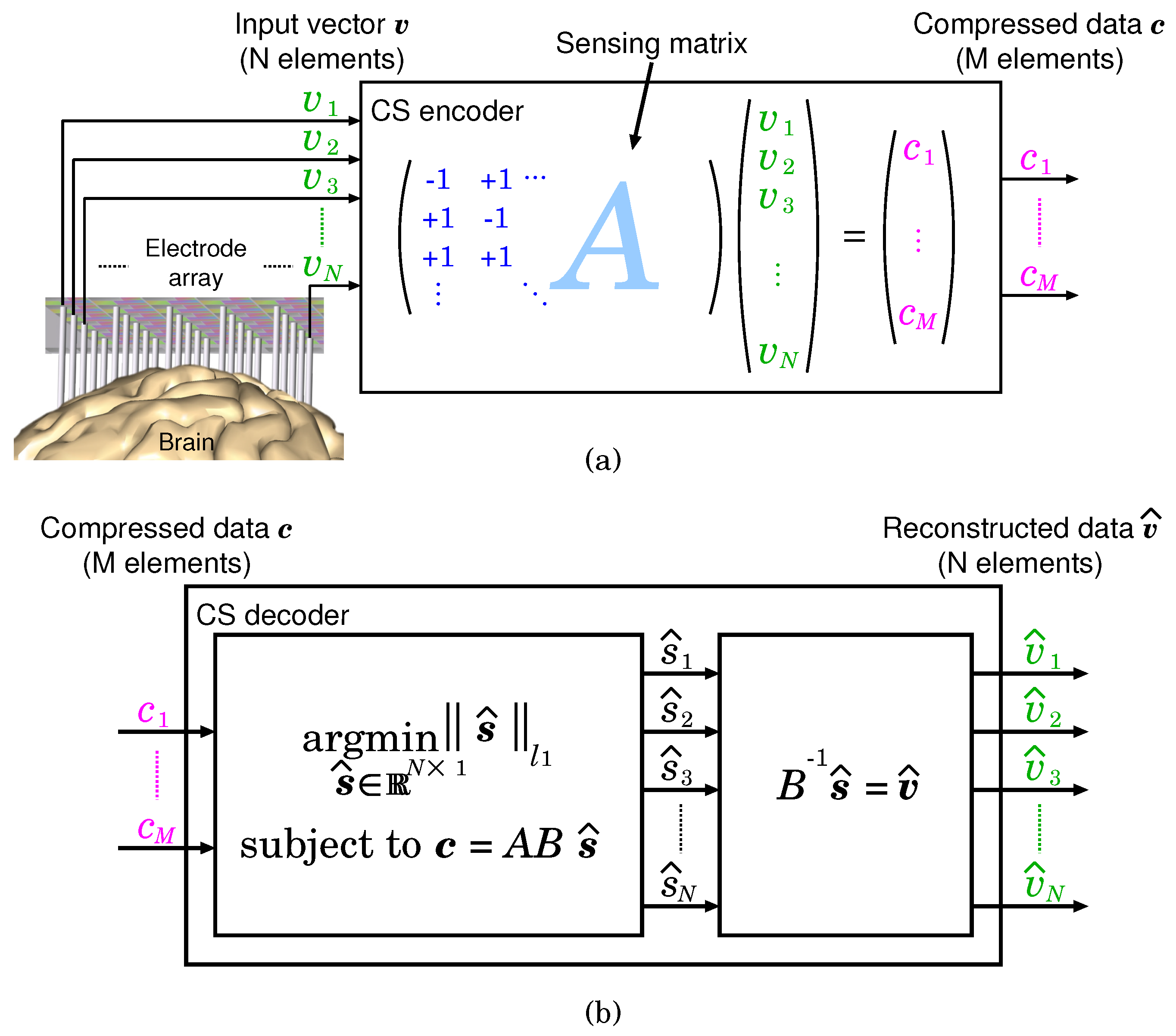
2. Theoretical Background of CS
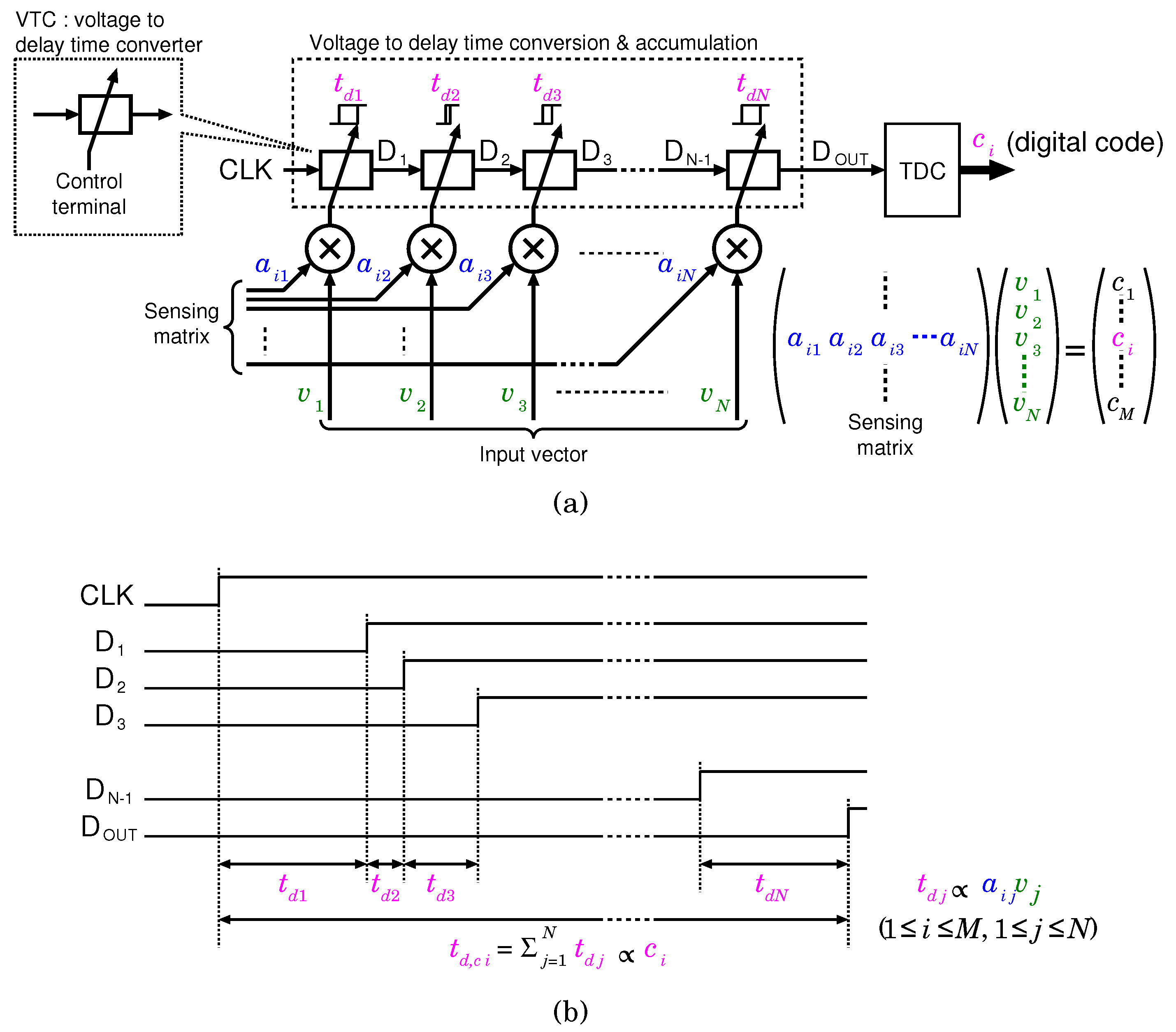
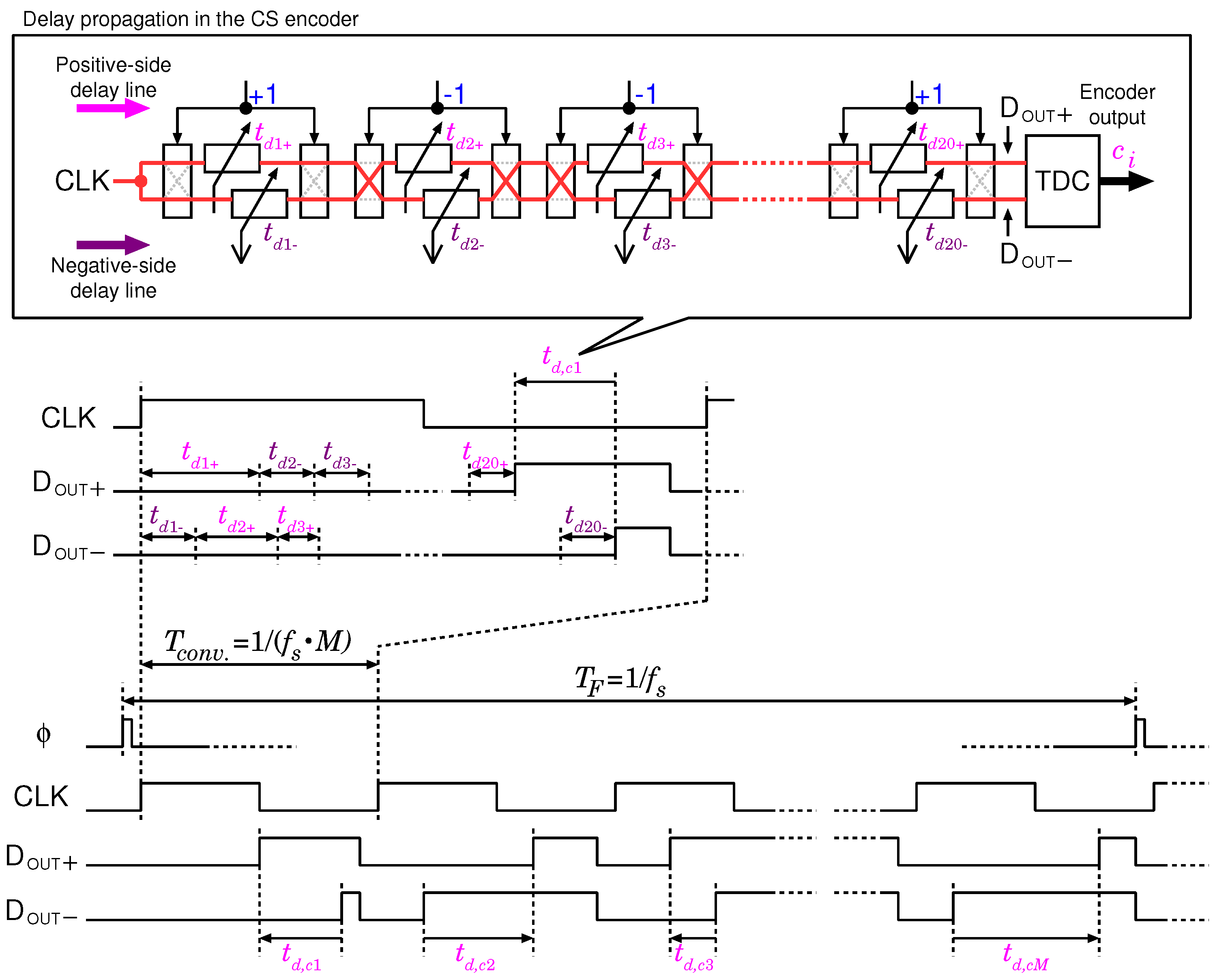
3. Time Domain Analog Signal Processing for CS Encoder
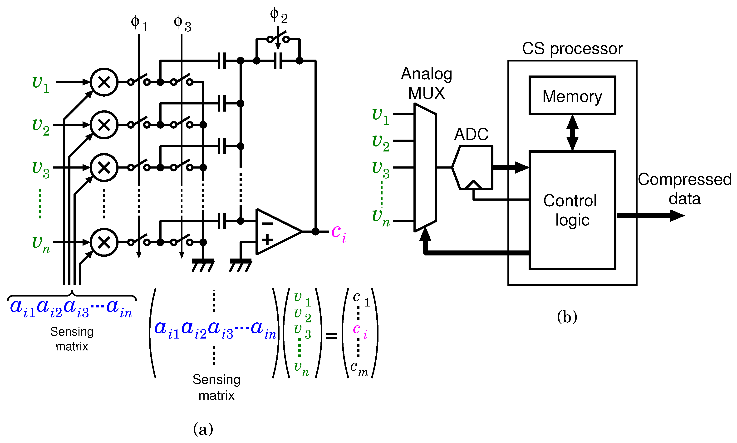
4. Design of the Proposed CS Encoder
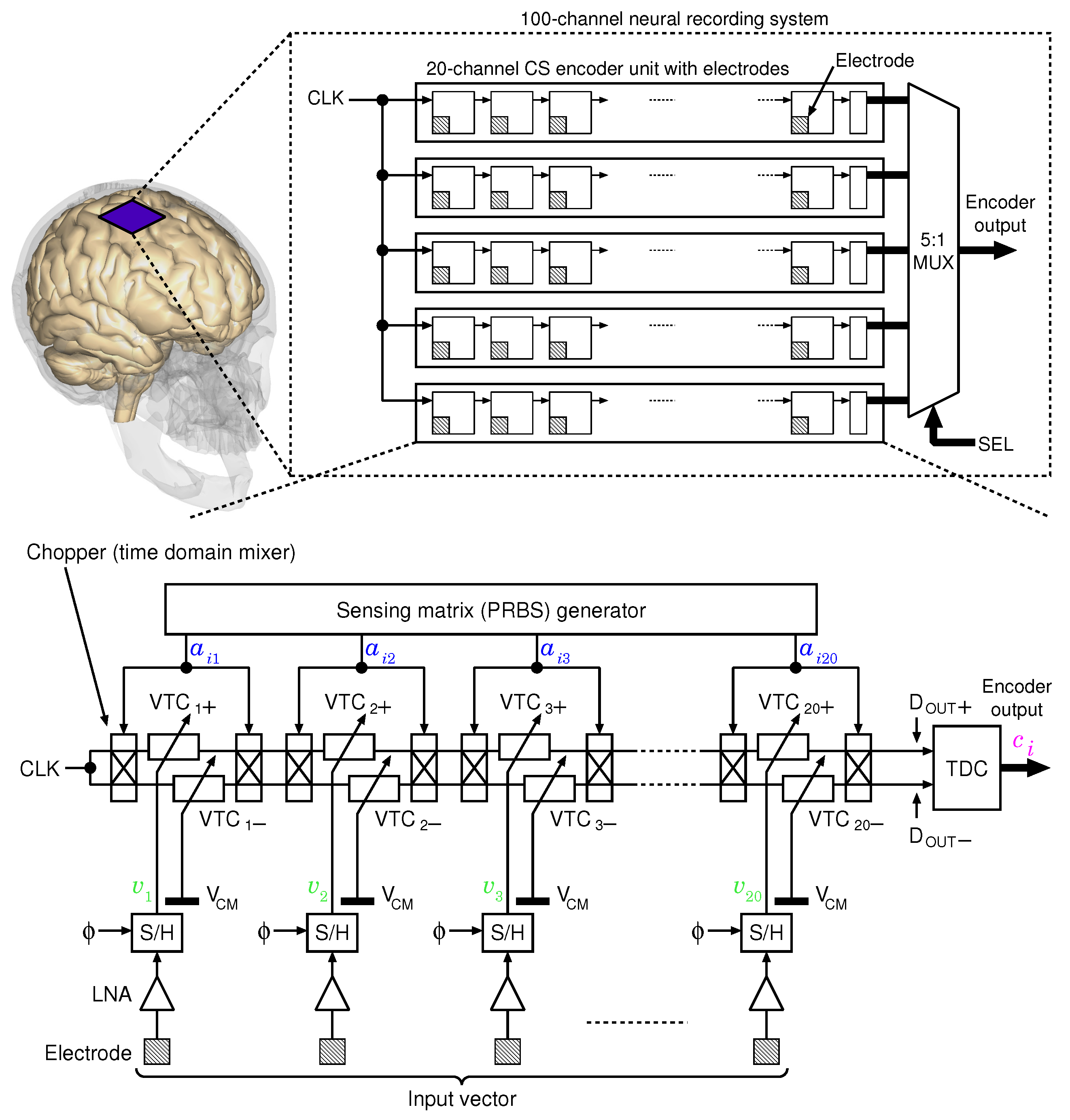
4.1. Overview of the Entire Operation
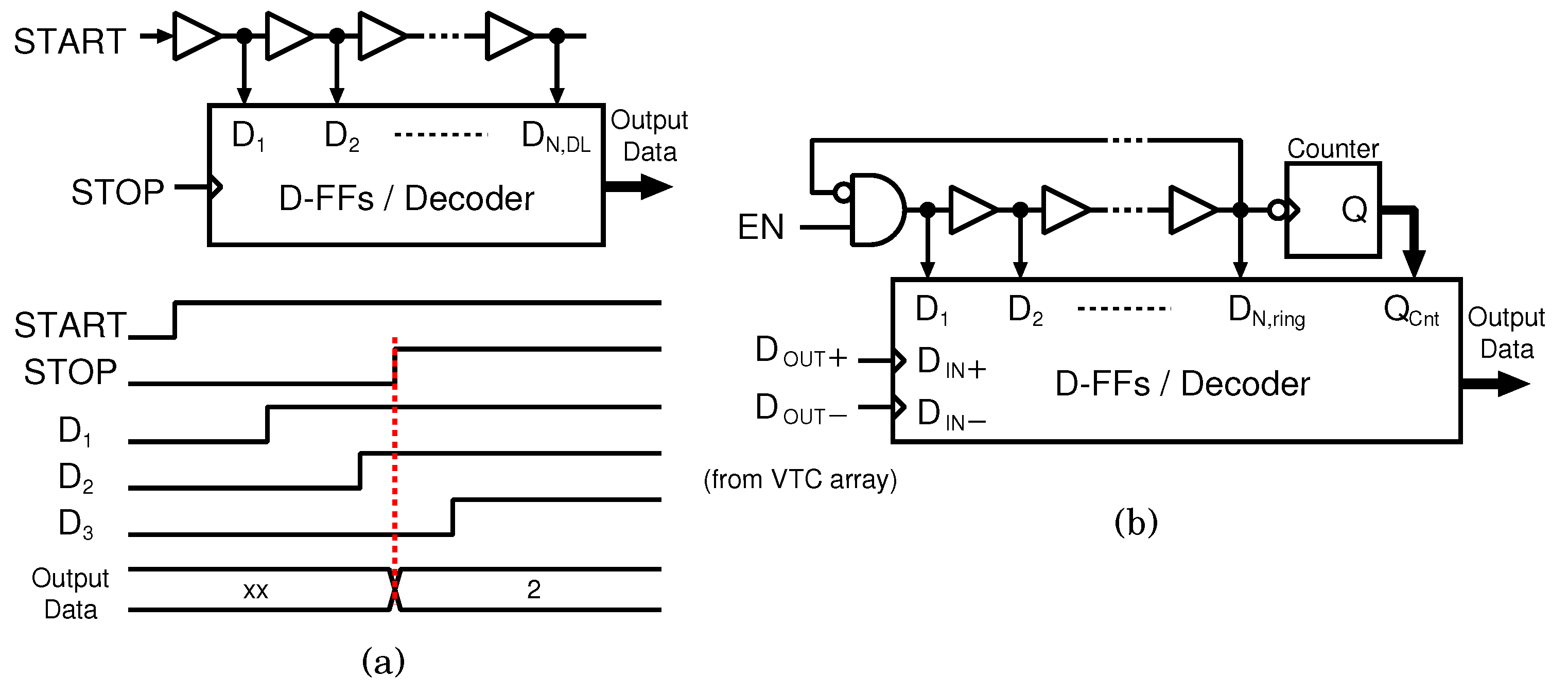
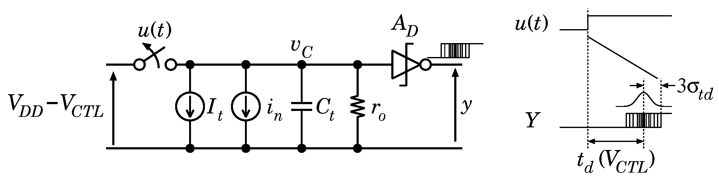
4.2. TDC
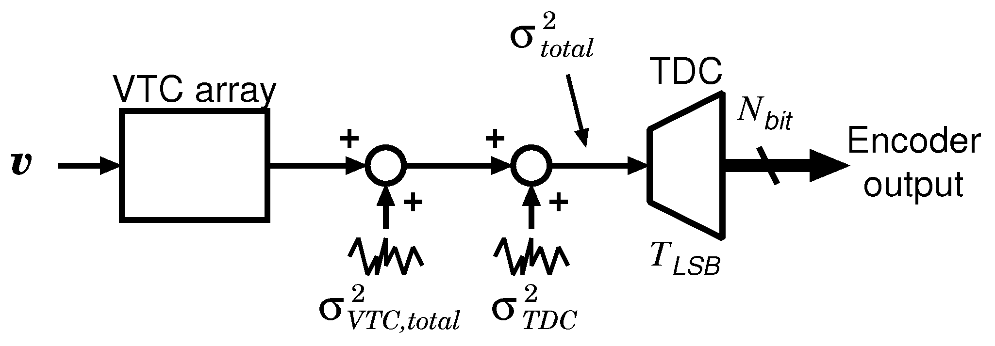
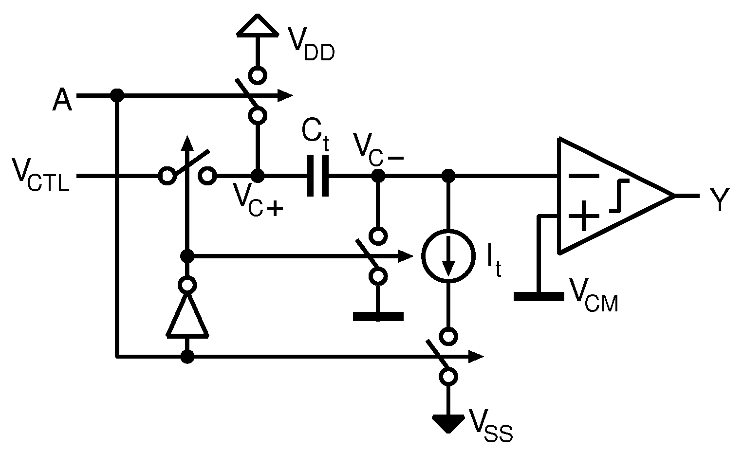
4.3. VTC
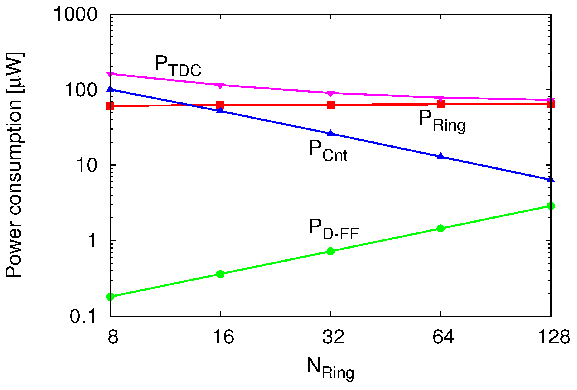
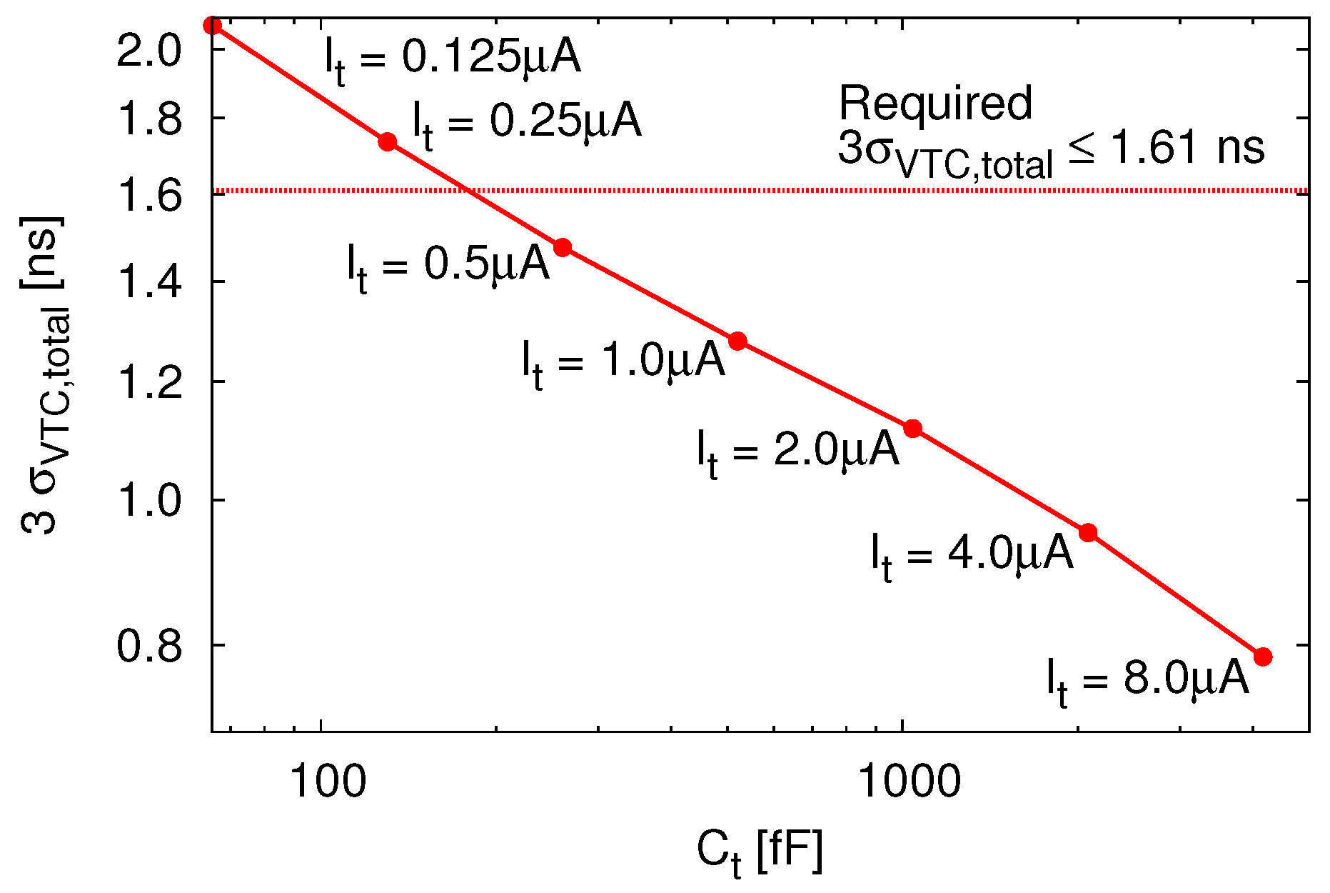
4.4. Design Constraints in Proposed Architecture
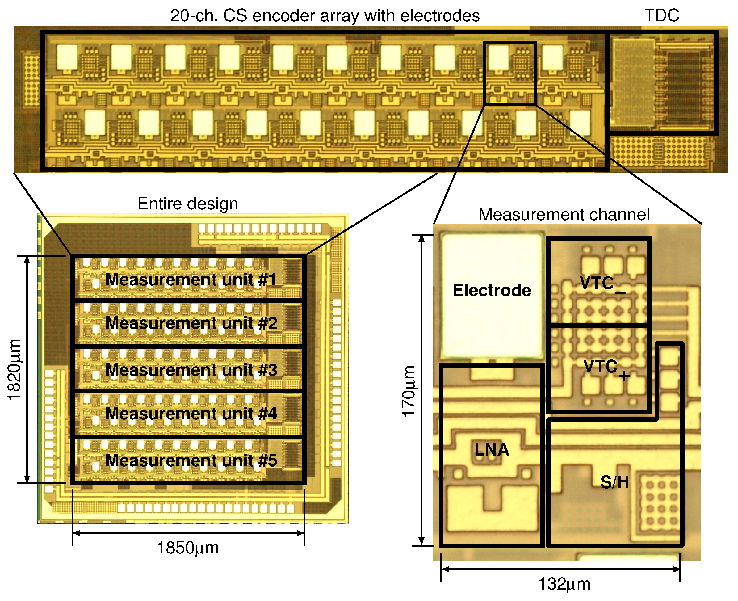
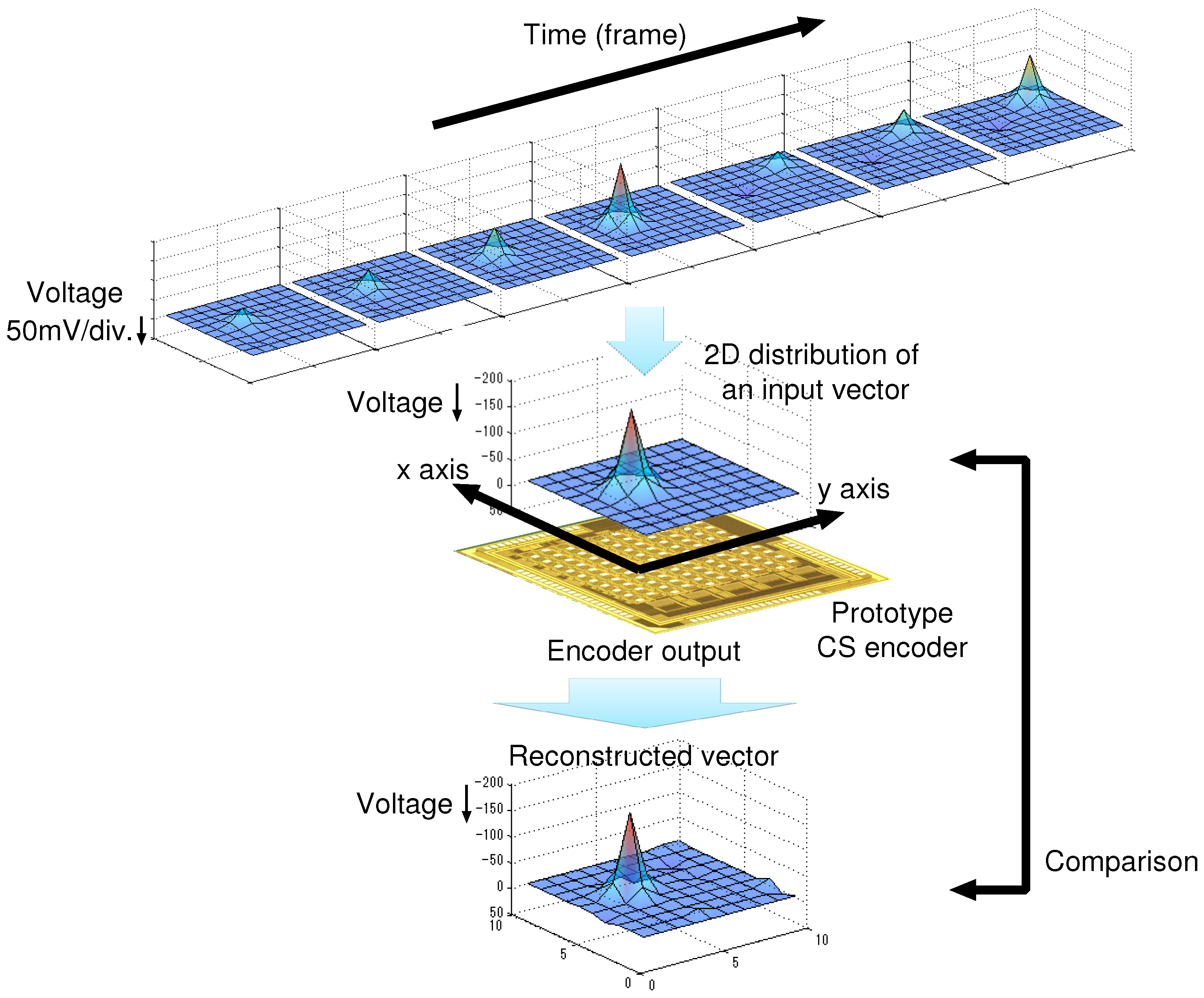
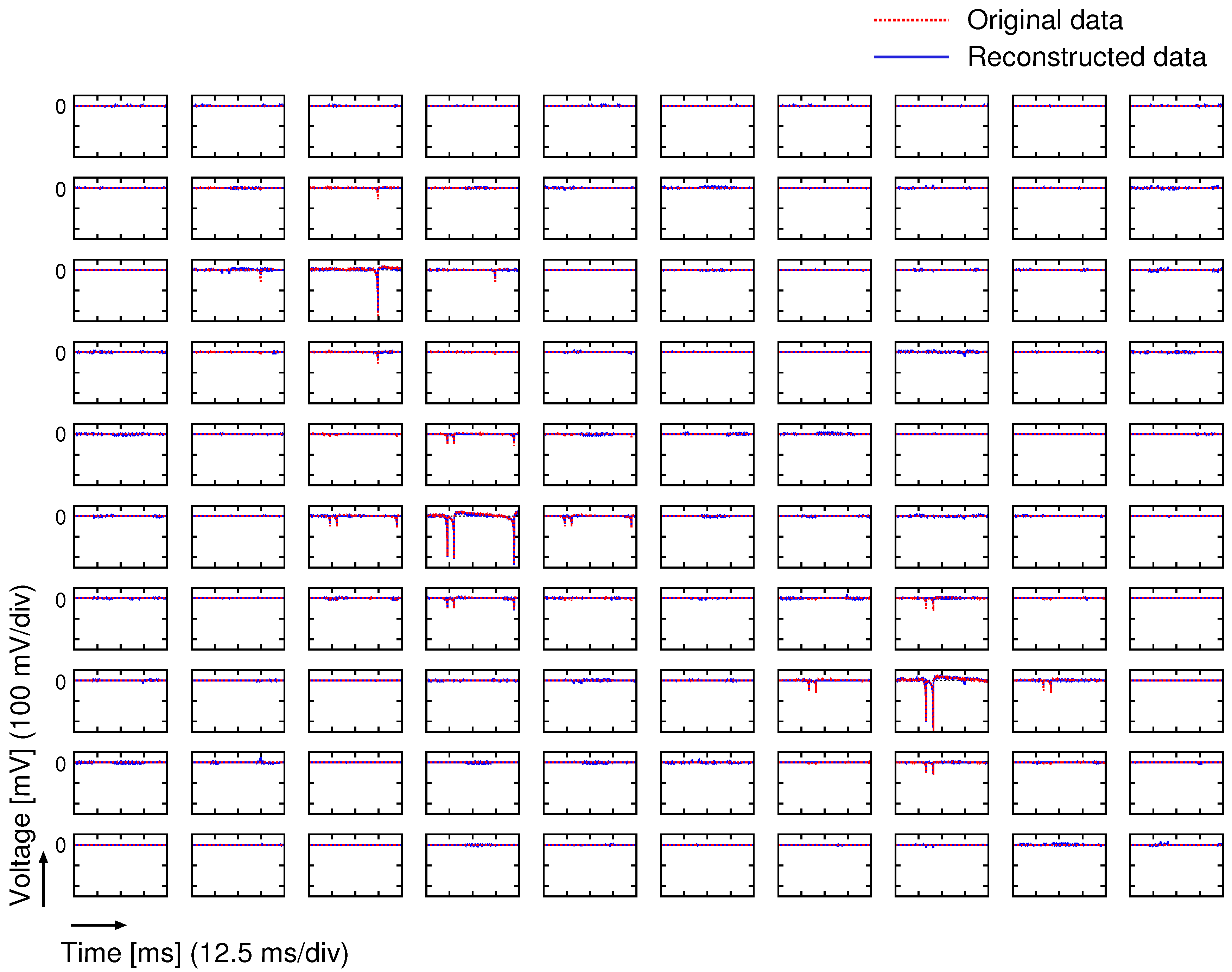
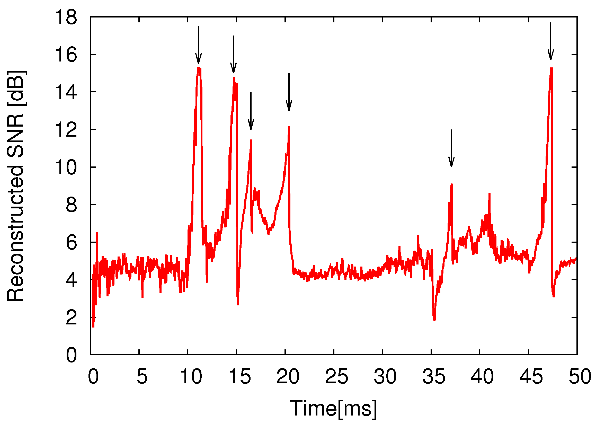
5. Measurement Results and Discussion
6. Conclusions
Acknowledgments
Author Contributions
Conflicts of Interest
Appendix A. Test Signal Generation

References
- HajjHassan, M.; Chodavarapu, V.; Musallam, S. NeuroMEMS: Neural probe microtechnologies. Sensors 2008, 8, 6704–6726. [Google Scholar] [CrossRef] [PubMed]
- Wise, K.D.; Angell, J.B.; Starr, A. An integrated-circuit approach to extracellular microelectrodes. IEEE Trans. Biomed. Eng. 1970, BME-17, 238–247. [Google Scholar] [CrossRef]
- Norlin, P.; Kindlundh, M.; Mouroux, A.; Yoshida, K.; Hofmann, U.G. A 32-site neural recording probe fabricated by DRIE of SOI substrates. J. Micromech. Microeng. 2002, 12, 414–419. [Google Scholar] [CrossRef]
- Kindlundh, M.; Norlin, P.; Hofmann, U.G. A neural probe process enabling variable electrode configurations. Sens. Actuators B Chem. 2004, 102, 51–58. [Google Scholar] [CrossRef]
- Harrison, R.R.; Watkins, P.T.; Kier, R.J.; Lovejoy, R.O.; Black, D.J.; Greger, B.; Solzbacher, F. A low-power integrated circuit for a wireless 100-electrode neural recording system. IEEE J. Solid-State Circuits 2007, 42, 123–133. [Google Scholar] [CrossRef]
- Harrison, R.R.; Kier, R.J.; Chestek, C.A.; Gilja, V.; Nuyujukian, P.; Ryu, S.; Greger, B.; Solzbacher, F.; Shenoy, K.V. Wireless neural recording with single low-power integrated circuit. IEEE Trans. Neural Syst. Rehab. Eng. 2009, 17, 322–329. [Google Scholar] [CrossRef] [PubMed]
- Shahrokhi, F.; Abdelhalim, K.; Serletis, D.; Carlen, P.L.; Genov, R. The 128-channel fully differential digital integrated neural recording and stimulation interface. IEEE Trans. Biomed. Circuits Syst. 2010, 4, 149–161. [Google Scholar] [CrossRef] [PubMed]
- Yin, M.; Borton, D.A.; Aceros, J.; Patterson, W.R.; Nurmikko, A.V. A 100-channel hermetically sealed implantable device for chronic wireless neurosensing applications. IEEE Trans. Biomed. Circuits Syst. 2013, 7, 115–128. [Google Scholar] [CrossRef] [PubMed]
- Schwarz, D.A.; Lebedev, M.A.; Hanson, T.L.; Dimitrov, D.F.; Lehew, G.; Meloy, J.; Rajangam, S.; Subramanian, V.; Ifft, P.J.; Li, Z.; et al. Chronic, wireless recordings of large scale brain activity in freely moving rhesus monkeys. Nat. Methods 2014, 11, 670–676. [Google Scholar] [CrossRef] [PubMed]
- Johnson, B.C.; Gambini, S.; Izyumin, I.; Moin, A.; Zhou, A.; Alexandrov, G.; Santacruz, S.R.; Rabaey, J.M.; Carmena, J.M.; Muller, R. An implantable 700 μW 64-channel neuromodulation IC for simultaneous recording and stimulation with rapid artifact recovery. In Proceedings of the 2017 Symposium on VLSI Circuits, Kyoto, Japan, 5–8 June 2017; pp. C48–C49. [Google Scholar]
- Sodagar, A.M.; Wise, K.D.; Najafi, K. A fully integrated mixed-signal neural processor for implantable multichannel cortical recording. IEEE Trans. Biomed. Eng. 2007, 54, 1075–1088. [Google Scholar] [CrossRef] [PubMed]
- Sodagar, A.M.; Perlin, G.E.; Yao, Y.; Najafi, K.; Wise, K.D. An implantable 64-channel wireless microsystem for single-unit neural recording. IEEE J. Solid-State Circuits 2009, 44, 2591–2604. [Google Scholar] [CrossRef]
- Lee, S.B.; Lee, H.M.; Kiani, M.; Jow, U.M.; Ghovanloo, M. An inductively powered scalable 32-channel wireless neural recording system-on-a-chip for neuroscience applications. IEEE Trans. Biomed. Circuits Syst. 2010, 4, 360–371. [Google Scholar] [CrossRef]
- Du, J.; Blanche, T.J.; Harrison, R.R.; Lester, H.A.; Masmanidis, S.C. Multiplexed, high density electrophysiology with nanofabricated neural probes. PLoS ONE 2011, 6, e26204. [Google Scholar] [CrossRef] [PubMed]
- Bagheri, A.; Gabran, S.R.I.; Salam, M.T.; Velazquez, J.L.P.; Mansour, R.R.; Salama, M.M.A.; Genov, R. Massively-parallel neuromonitoring and neurostimulation rodent headset with nanotextured flexible microelectrodes. IEEE Trans. Biomed. Circuits Syst. 2013, 7, 601–609. [Google Scholar] [CrossRef] [PubMed]
- Lopez, C.M.; Andrei, A.; Mitra, S.; Welkenhuysen, M.; Eberle, W.; Bartic, C.; Puers, R.; Yazicioglu, R.F.; Gielen, G. An implantable 455-active-electrode 52-channel CMOS neural probe. IEEE J. Solid State Circuits 2014, 49, 248–261. [Google Scholar] [CrossRef]
- Zoladz, M.; Kmon, P.; Rauza, J.; Grybos, P.; Blasiak, T. Multichannel neural recording system based on family ASICs processed in submicron technology. Microelectronics J. 2014, 45, 1226–1231. [Google Scholar] [CrossRef]
- Park, S.Y.; Cho, J.; Yoon, E. 3.37 μW/Ch Modular Scalable Neural Recording System with Embedded Lossless Compression for Dynamic Power Reduction. In Proceedings of the 2017 Symposium on VLSI Circuits, Kyoto, Japan, 5–8 June 2017; pp. C168–C169. [Google Scholar]
- Han, D.; Zheng, Y.; Rajkumar, R.; Dawe, G.S.; Je, M. A 0.45 V 100-channel neural-recording IC with sub-μW/channel consumption in 0.18 CMOS. IEEE Trans. Biomed. Circuits Syst. 2013, 7, 735–746. [Google Scholar] [CrossRef] [PubMed]
- Frey, U.; Sedivy, J.; Heer, F.; Pedron, R.; Ballini, M.; Mueller, J.; Bakkum, D.; Hafizovic, S.; Faraci, F.D.; Greve, F.; et al. Switch-matrix-based high-density microelectrode array in CMOS technology. IEEE J. Solid-State Circuits 2010, 45, 467–482. [Google Scholar] [CrossRef]
- Frey, U.; Egert, U.; Heer, F.; Hafizovic, S.; Hierlemann, A. Microelectronic system for high-resolution mapping of extracellular electric fields applied to brain slices. Biosens. Bioelectron. 2009, 24, 2191–2198. [Google Scholar] [CrossRef] [PubMed]
- Chae, M.S.; Yang, Z.; Yuce, M.R.; Hoang, L.; Liu, W. A 128-channel 6 mW wireless neural recording IC with spike feature extraction and UWB transmitter. IEEE Trans. Neural Syst. Rehab. Eng. 2009, 17, 312–321. [Google Scholar] [CrossRef] [PubMed]
- Ando, H.; Takizawa, K.; Yoshida, T.; Matsushita, K.; Hirata, M.; Suzuki, T. Wireless multichannel neural necording with a 128-Mbps UWB transmitter for an implantable brain-machine interfaces. IEEE Trans. Biomed. Circuits Syst. 2016, 10, 1068–1078. [Google Scholar] [CrossRef] [PubMed]
- Stevenson, I.H.; Kording, K.P. How advances in neural recording affect data analysis. Nat. Neurosci. 2011, 14, 139–142. [Google Scholar] [CrossRef] [PubMed]
- Gosselin, B. Recent advances in neural recording microsystems. Sensors 2011, 11, 4572–4597. [Google Scholar] [CrossRef] [PubMed]
- Donoho, D.L. Compressed sensing. IEEE Trans. Info. Theory 2006, 52, 1289–1306. [Google Scholar] [CrossRef]
- Candes, E.J.; Tao, T. Near-optimal signal recovery from random projections: Universal encoding strategies? IEEE Trans. Inf. Theory 2006, 52, 5406–5425. [Google Scholar] [CrossRef]
- Chen, F.; Chandrakasan, A.P.; Stojanović, V.M. Design and analysis of a hardware-efficient compressed sensing architecture for data compression in wireless sensors. IEEE J. Solid State Circ. 2012, 47, 744–756. [Google Scholar] [CrossRef]
- Sun, C.; Li, W.; Chen, W. A compressed sensing based method for reducing the sampling time of a high resolution pressure sensor array system. Sensors 2017, 17, 1848. [Google Scholar] [CrossRef] [PubMed]
- Tseng, Y.; Chen, Y. Adaptive integration of the compressed algorithm of CS and NPC for the ECG signal compressed algorithm in VLSI implementation. Sensors 2017, 17, 2288. [Google Scholar] [CrossRef] [PubMed]
- Liu, X.; Zhu, H.; Zhang, M.; Richardson, A.G.; Lucas, T.H.; Spiegel, J.V. Design of a low-noise, high power efficiency neural recording front-end with an integrated real-time compressed sensing unit. In Proceedings of the 2015 IEEE International Symposium on Circuits and Systems (ISCAS), Lisbon, Portugal, 24–27 May 2015; pp. 2996–2999. [Google Scholar]
- Liu, X.; Zhang, M.; Xiong, T.; Richardson, A.G.; Lucas, T.H.; Chin, P.S.; Etienne-Cummings, R.; Tran, T.D.; Spiegel, J.V. A fully integrated wireless compressed sensing neural signal acquisition system for chronic recording and brain machine interface. IEEE Trans. Biomed. Circuits Syst. 2016, 10, 874–883. [Google Scholar] [CrossRef] [PubMed]
- Shoaran, M.; Kamal, M.H.; Pollo, C.; Vandergheynst, P.; Schmid, A. Compact low-power cortical recording architecture for compressive multichannel data acquisition. IEEE Trans. Biomed. Circuits Syst. 2014, 8, 857–870. [Google Scholar] [CrossRef] [PubMed]
- Shoaran, M.; Lopez, M.M.; Pasupureddi, V.S.R.; Leblebici, Y.; Schmid, A. A low-power area-efficient compressive sensing approach for multi-channel neural recording. In Proceedings of the 2013 IEEE International Symposium on Circuits and Systems, Beijing, China, 19–23 May 2013; pp. 2191–2194. [Google Scholar] [CrossRef]
- Oike, Y.; Gamal, A.E. CMOS image sensor with per-column ΣΔ ADC and programmable compressed sensing. IEEE J. Solid State Circuits 2013, 48, 318–328. [Google Scholar] [CrossRef]
- Wu, L.; Yu, K.; Cao, D.; Hu, Y.; Wang, Z. Efficient sparse signal transmission over a lossy link using compressive sensing. Sensors 2015, 15, 19880–19911. [Google Scholar] [CrossRef] [PubMed]
- Balouchestani, M.; Krishnan, S. Effective low-power wearable wireless surface EMG sensor design based on analog-compressed sensing. Sensors 2014, 14, 24305–24328. [Google Scholar] [CrossRef] [PubMed]
- Pant, J.; Lu, W.; Antoniou, A. new improved algorithms for compressive sensing based on lp Norm. IEEE Trans. Circuits Syst. 2014, 61, 198–202. [Google Scholar] [CrossRef]
- Zhang, Z.; Rao, B.D. Extension of SBL algorithms for the recovery of block sparse signals with intra-block correlation. IEEE Trans. Signal Proc. 2013, 61, 2009–2015. [Google Scholar] [CrossRef]
- Sepke, T.; Holloway, P.; Sodini, C.G.; Lee, H.S. Noise analysis for comparator-based circuits. IEEE Trans. Circuits Syst. I 2009, 56, 541–553. [Google Scholar] [CrossRef]
- Hajimiri, A.; Limotyrakis, S.; Lee, T.H. Jitter and phase noise in ring oscillators. IEEE J. Solid State Circuits 1999, 34, 790–804. [Google Scholar] [CrossRef]
- Grant, M.C.; Boyd, S.P. CVX: Matlab Software for Disciplined Convex Programming. Available online: http://cvxr.com/cvx/ (accessed on 11 October 2017).
- Hosseini-Nejad, H.; Jannesari, A.; Sodagar, A.M.; Rodrigues, J.N. A 128-channel discrete cosine transform-based neural signal processor for implantable neural recording microsystems. Int. J. Circuit Theory Appl. 2015, 43, 489–501. [Google Scholar] [CrossRef]
- Lewicki, M. A review of methods for spike sorting: The detection and classification of neural action potentials. Netw. Comput. Neural Syst. 1998, 9, R53–R78. [Google Scholar] [CrossRef]
- Delgado-Restituto, M.; Rodriguez-Perez, A.; Darie, A.; Soto-Sanchez, C.; Fernandez-Jover, E.; Rodriguez-Vazquez, A. System-level design of a 64-channel low power neural spike recording sensor. IEEE Trans. Biomed. Circuits Syst. 2017, 11, 420–433. [Google Scholar] [CrossRef] [PubMed]
- Aharon, M.; Elad, M.; Bruckstein, A. K-SVD: An algorithm for designing overcomplete dictionaries for sparse representation. IEEE Trans. Signal Process. 2006, 54, 4311–4322. [Google Scholar] [CrossRef]
- Mangia, M.; Pareschi, F.; Cambareri, V.; Rovatti, R.; Setti, G. Rakeness-Based Design of Low-Complexity Compressed Sensing. IEEE Trans. Circuits Syst. I 2017, 64, 1201–1213. [Google Scholar] [CrossRef]
- Izhikevich, E.M. Simple model of spiking neurons. IEEE Trans. Neural Netw. 2003, 14, 1569–1572. [Google Scholar] [CrossRef] [PubMed]
- Hodgkin, A.L.; Huxley, A.F. A quantitative description of membrane current and its application to conduction and excitation in nerve. Bull. Math. Biol. 1990, 52, 25–71. [Google Scholar] [CrossRef] [PubMed]
- Nunez, P.L.; Srinivasan, R. Electric Fields of the Brain: The neurophysics of EEG, 2nd ed.; Oxford University Press: New York, NY, USA, 2006; ISBN 9780195050387. [Google Scholar]


| Parameter | [28] | [31] | [32] | [33] | [34] | This Work |
|---|---|---|---|---|---|---|
| (Simulated) | ||||||
| Technology [nm] | 90 | 180 | 180 | 180 | 180 | 180 |
| Number of channels | 1 | 12 | 16 | 16 | 16 | 100 |
| Target signal type | EEG | Neural signal | LFP / AP | EEG | AP | AP |
| Input signal BW [kHz] | 10 | 7 | 10 | 2 | 10 | 10 |
| Resolution [bit] | 8 | 12 | 10 | 10 | - | 10 |
| Implementation method | Digital CS | Digital CS | Digital CS | Analog CS | Analog CS | Time-domain analog CS |
| Input vector type | Temporal | Temporal | Temporal | Spatial | Spatial | Spatial |
| Compression ratio (CR) | 20 | 8–16 | 2.3 | 1–20 | ||
| Reconstructed SNR [dB] | 10 (CR = 20) | - | 9.78 (CR = 8) | 10.9 (CR = 4) | 6.47 (CR = 2.3) | 15.3 (CR = 4) |
| Total area [] | 0.104 (w/o LNA) | 0.563 | 0.0489 | 0.0464 | - | 0.0331 |
| CS encoder area (w/o AFE) [] | 0.09 | - | 0.0117 | 0.008 | 0.0023 | 0.0065 |
| Total power efficiency [] | - | - | 475 (CR = 8) | 238 (CR = 4) | 343.5 (CR = 2.3) | 92.6 (CR = 4) |
| CS encoder power efficiency (w/o AFE) [] | - | - | 241 (CR = 8) | 131 (CR = 4) | 53.5 (CR = 2.3) | 25.0 (CR = 4) |
© 2018 by the authors. Licensee MDPI, Basel, Switzerland. This article is an open access article distributed under the terms and conditions of the Creative Commons Attribution (CC BY) license (http://creativecommons.org/licenses/by/4.0/).
Share and Cite
Okazawa, T.; Akita, I. A Time-Domain Analog Spatial Compressed Sensing Encoder for Multi-Channel Neural Recording. Sensors 2018, 18, 184. https://doi.org/10.3390/s18010184
Okazawa T, Akita I. A Time-Domain Analog Spatial Compressed Sensing Encoder for Multi-Channel Neural Recording. Sensors. 2018; 18(1):184. https://doi.org/10.3390/s18010184
Chicago/Turabian StyleOkazawa, Takayuki, and Ippei Akita. 2018. "A Time-Domain Analog Spatial Compressed Sensing Encoder for Multi-Channel Neural Recording" Sensors 18, no. 1: 184. https://doi.org/10.3390/s18010184
APA StyleOkazawa, T., & Akita, I. (2018). A Time-Domain Analog Spatial Compressed Sensing Encoder for Multi-Channel Neural Recording. Sensors, 18(1), 184. https://doi.org/10.3390/s18010184