Abstract
In this work, a low cost Bluetooth Low Energy (BLE) transceiver for wireless sensor network (WSN) applications, with a receiver (RX) matching network reusing power amplifier (PA) load inductor, is presented. In order to decrease the die area, only two inductors were used in this work. Besides the one used in the voltage control oscillator (VCO), the PA load inductor was reused as the RX impedance matching component in the front-end. Proper controls have been applied to achieve high transmitter (TX) input impedance when the transceiver is in the receiving mode, and vice versa. This allows the TRX-switch/matching network integration without significant performance degradation. The RX adopted a low-IF structure and integrated a single-ended low noise amplifier (LNA), a current bleeding mixer, a 4th complex filter and a delta-sigma continuous time (CT) analog-to-digital converter (ADC). The TX employed a two-point PLL-based architecture with a non-linear PA. The RX achieved a sensitivity of −93 dBm and consumes 9.7 mW, while the TX achieved a 2.97% error vector magnitude (EVM) with 9.4 mW at 0 dBm output power. This design was fabricated in a 0.11 μm complementary metal oxide semiconductor (CMOS) technology and the front-end circuit only occupies 0.24 mm2. The measurement results verify the effectiveness and applicability of the proposed BLE transceiver for WSN applications.
1. Introduction
There has been an explosive growth recently in wireless sensor networks (WSN) [1], whose applications have been extended to autonomous health monitoring, remote or hazardous area monitoring, and emergency management. The sensor nodes in these networks are typically connected to multiple types of devices, including smartphones, wearables and PCs [2]. For the sake of flexibility, low cost and seamlessness, the communication among these nodes requires the use of a commonly or easily available wireless technique. Therefore, Bluetooth Low Energy (BLE) is a competitive candidate [3,4] because of its already massive establishment in the mobile market.
Due to the limited energy source (e.g., battery or harvested energy) of the sensor nodes, an ultra-low power (ULP) transceiver design for WSN applications is highly desirable. In addition, because of the stringent market requirements, there has been a strong drive in recent years to decrease the cost and module area of wireless sensor nodes [5]. This can be achieved through shrinking the silicon area and reducing the external components. Therefore, the investigation on low power and low cost BLE transceivers is indispensable.
For a conventional radio frequency (RF) front-end configuration [6] as shown in Figure 1, there are several external components: (1) the impedance matching network for the low noise amplifier (LNA); (2) the TRX-antenna switch; and (3) impedance matching network for the power amplifier (PA). This leads to an increase in the printed circuit board (PCB) area and cost. For a low cost BLE module, these external TRX-switches and matching networks [6,7] are clearly not favorable. To achieve higher integration, an on-chip CMOS TRX-switch technique has been reported in [8], yet the non-linearity and insertion loss introduced by CMOS transistors will deteriorate the performance of the transceiver. In [9,10,11], an on-chip balun shared by the transmitter (TX) and receiver (RX) was used to convert the single-ended signal to a differential one, and eliminated the need of a separated TRX-switch through the principle of impedance conversion. However, the differential architectures for both LNA and PA is power-consuming for an ultra-low power transceiver. Meanwhile, the insertion loss of the on-chip balun will degrade RX noise figure (NF). In [12,13], a TRX-switch and matching network were integrated using multiple inductors, which is area-consuming and thus not favorable in low cost design.
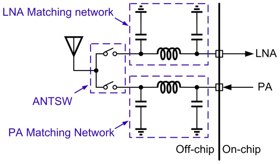
Figure 1.
The conventional RF front-end configuration.
To address the aforementioned issues, a low power and low cost transceiver for 2.4 GHz ISM band was presented in this work. Seeking a low-power implementation, a single-ended LNA and PA were employed in the transceiver. In order to further reduce the chip cost and module area, a front-end with a RX matching network reusing PA load inductor was proposed.
2. Proposed Front-End with RX Matching Network Reusing PA Load Inductor
An integrated TRX-switch/matching network presents some design challenges. Firstly, reliability issues will be introduced by the large PA output power through stressing the low noise amplifier (LNA) input transistors. This requires an input voltage swing reduction of LNA at TX mode, and thus a large RX off-state impedance (ZRX-off). Secondly, the TX performance features, such as output power, error vector magnitude (EVM) should not be degraded by the ZRX-off. Similarly and finally, the off-state TX impedance (ZTX-off) should not deteriorate RX performance such as NF and linearity.
BLE specification asks for only −70 dBm sensitivity (1-MHz channel bandwidth) at GFSK modulation with a required SNR of 14 dB [4]. The NF can thus be obtained by:
where BW and SNRout represent channel bandwidth and required demodulator signal-to-noise ratio (SNR), respectively. The maximum allowable NF obtained using (1) is 30 dB. However, in order to increase the link budget, a NF below 7 dB was targeted in this work. This allows a reasonable matching network design trade-off between RX noise and power delivery.
NF = −(−174 dBm/Hz) − 10 × Log(BW) − SNRout + Sensitivity,
Figure 2a shows the simplified schematic of the proposed front-end with RX matching network reusing PA load inductor. The front-end integrated the TRX-switch and matching network. The PA load inductor L1 is reused as the impedance matching component for RX. Capacitors C1 and C2 are employed to match the impedance in both RX and TX paths. Switches S1–S9 are adopted to determine the mode of the front-end circuit.
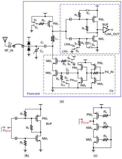
Figure 2.
(a) Proposed front-end with RX matching network reusing PA load inductor; (b) Simplified LNA circuit in TX mode; (c) Simplified PA circuit in RX mode.
In TX mode, S1, S4, S7, S5 and S9 are turned off while S2, S3, S5, S8 and S9 are turned on. The inductor L1 acts as the load of the PA which is typically supplied by DC-DC convertor through the PM2. For PM2 size, it is determined by the following three factors: (1) The on-resistance. Large on-resistance causes a large voltage drop, and thus reduces the efficiency of PA. (2) The parasitic resistance and capacitance when PM2 is turned off. RX NF might thus be degraded. (3) The current density. The size of PM2 should be large to accommodate large PA current. Therefore, the size of PM2 is chosen to be 0.11 μm/200 μm, where the width is 5 μm and the finger number is 40. For LNA, the input transistors NM1 and PM1 are turned off and the simplified circuit is shown in Figure 2b. Consequently, the PA sees the impedance of the LNA path (ZRX-off) as a small capacitor shunted with a large resistor given as RRL‖1/jωCRL. Around 2.45 GHz, simulation shows the real and imaginary parts of ZRX-off are 2.6 kΩ and 95 fF, respectively. Simulation shows about 4% PA efficiency loss due to ZRX-off and PM2.
In RX mode, S1, S4, S7, S5 and S9 are turned on and S2, S3, S5, S8 and S9 are turned off. For PA, the transistors (NM2, NM3 and PM2) are turned off and the simplified circuit is shown in Figure 2c. Similarly, LNA sees PA path as a large impedance (ZTX-off), consisting of a small capacitor shunted with a large resistor and can be given as ZTX-off = RTL‖1/jωCTL. Around 2.45 GHz, the simulated real and imaginary parts of ZTX-off are 16 kΩ and 66 fF, respectively. This large impedance ZTX-off results in a 0.4 dB insertion loss, which is acceptable for the NF requirement of BLE.
2.1. PA and PA Matching Network
In the TX, a switching-type single-ended PA operating in non-linear region is employed for the constant envelope modulation required by BLE, as shown in Figure 2a. The PA is typically powered by a DC-DC convertor with reduced output noise [14,15] for better PA linearity. This PA composes of three stages of amplification, with two inverters as pre-amplifiers for the gate voltage of NM2. For the first one, it is placed in proximity to VCO to drive the long signal path between VCO and PA. For the second one, it does not generate a rail-to-rail output signal. The final stage is a cascode-type amplifier, where NM2 adopts thin gate oxide to obtain input/output isolation. The cascode stage NM3 increases the output impedance of the PA and employs thick gate oxide to withstand peak drain voltage beyond power supply due to the inductive load [16]. The size of the second inverter, together with NM2 size and NM2 gate bias, are carefully chosen to obtain the input signal of NM2 with appropriate amplitude and operation point, which reduce 2nd harmonic component while maintain the required output power. Simultaneously, 2nd harmonic component is further attenuated by 15 dB with the matching network.
In TX mode, the simplified small signal equivalent circuit diagram of ZTX is shown in Figure 3, and the output impedance can be written as:
where RD represents the output impedance of the cascode NM2 and NM3, RI represents the shunt resistance of the inductor, Ccr represents the sum of various parasitic capacitances seen from the output. The value of L should be large to increase output power and make ZTX in inductive region in Smith chart, as shown in Figure 4a. Therefore, ZTX can be simplified as a resistor Rt shunted with an inductor Lt, and the admittance YTX can be written as:
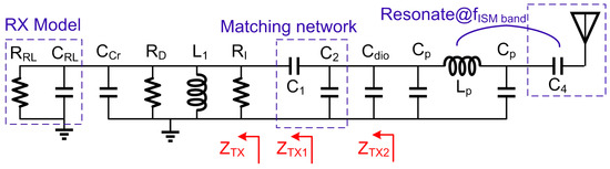
Figure 3.
TX matching network analysis.
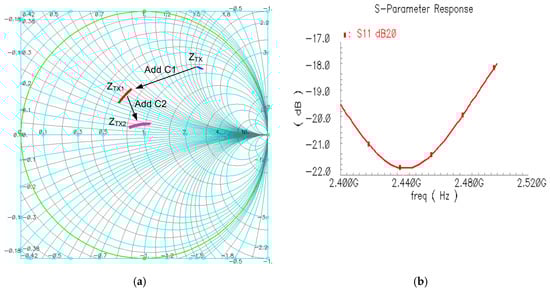
Figure 4.
TX impedance analysis. (a) TX impedance movement in Smith chart; (b) The final S11 of TX impedance from 2.4 GHz to 2.5 GHz.
Two additional matching components help to match ZTX to 50 Ω. Taking the compatibility with the RX matching network (mentioned below) into account, the matching network of a series capacitor C1 and a shunt capacitor C2 is selected. ZTX1 is the series impedance of ZTX and C1, and YTX2 is the shunt admittance of ZTX1 and C2, which are written as:
where Cdio represents the capacitance introduced by ESD diode. From (5) and (6), the value of C1 and C2 can be obtained if the output impedance is matched to 50 Ω, and Figure 4a shows the trajectory of the ZTX when applying C1 and C2. Another factor needs to be considered is bonding wire which can be simply modeled as two capacitors shunted with an inductor. The inductance of the bonding wire can be cancelled by its resonating with the output decoupling cap C4 at 2.45 GHz. As shown in Figure 4b, the overall simulated TX impedance S11 is smaller than −18 dB within in ISM band.
2.2. LNA and LNA Matching Network
To allow the RX a good coexistence performance with an in-band blocker [9], the LNA and mixer should be designed to be linear to prevent these blockers from degrading the performance. As shown in Figure 2, the LNA adopts a push-pull common-source inductorless topology [17], which inherently achieves higher linearity and power-efficiency when compared with a conventional NMOS-only LNA [18].
In RX mode, the simplified small signal equivalent circuit diagram of ZRX is shown in Figure 5, and the output impedance can be written as:
where Cct represents the sum of all of parasitic capacitances seen from the LNA input, Zin represents the LNA input impedance and can be expressed as [17]:
where Cgsn1 and Cgsp1 represent the capacitance between the gate and the source of NM1 and PM1, respectively. GV represents the LNA voltage gain and can be written as:
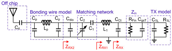
Figure 5.
RX matching network analysis.
Here gmn1 and gmp1 represent the transconductance of NM1 and NM2 respectively, and Rs is 50 Ω. Thus, ZRX can be simplified as a resistor Rr shunted with an inductor Cr, and the admittance YRX can be expressed as:
Considering there is no inductive device in the LNA circuit, ZRX is in the capacitive region in Smith chart. Therefore, the PA load inductor L1 is reused in RX matching network. As described above, L1 moves ZRX to the inductive region in Smith chart. ZRX1 represents the series impedance of ZRX and L1, which can be written as:
Then ZRX1 can be moved to near the center point via the capacitor C1 and trimming the capacitor C2. Figure 6 shows the trajectory of the ZRX when applying L1, C1 and C2. ZRX2 represents the impedance after adding C1 and C2, and can be expressed as:
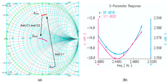
Figure 6.
(a) RX impedance movement in smith chart; (b) The final NF and S11 of RX impedance from 2.4 GHz to 2.5 GHz.
As shown in Figure 6b, the simulated LNA NF is around 2.57 dB and the maximum S11 is about −15 dB.
2.3. The Summarized Merits of this Proposed Frond-End
There are some merits of the proposed front-end with RX matching network reusing PA load inductor: (1) Only one inductor is employed in this front end. It is used for PA load in TX mode, and reused as a matching component in RX mode. Thus, the chip area has been reduced significantly; (2) The front-end has integrated the TRX-switch and matching network, and reduced the number of external components and thus reduced the cost of WSNs nodes; (3) RX and TX performance have not been deteriorated: for one, the impedance of LNA and PA can be optimized respectively using the proposed scheme; for the other thing, nonlinear components, such as CMOS switch, have not been adopted in the signal path of matching network; (4) It is free of TX reliability issues, because the PA sees the RX path as a high impedance compared with 50 Ω and the input voltage swing of the LNA is very small.
3. Transceiver Circuit Implementation
3.1. Transceiver Architecture
Recent designs for the 2.4 GHz ISM band receiver employed either the sliding-IF [19,20,21], direct conversion [22,23] or low-IF architecture [9], which have been demonstrated to be the most feasible to meet BLE performance requirements under severe power and chip area constraints. The sliding-IF architecture shifts the RF signal into the analog baseband (ABB) signal with twice frequency conversions [24,25]. This architecture facilitates LO generation and distribution at a favorably lower frequency, but causes a systematic, difficult-to-avoid susceptibility to out-of-band (around 1.45 GHz) image interference. Furthermore, GFSK modulation used in BLE contains significant energy at very low frequencies close to DC. Considering direct conversion architecture is susceptible to DC offset and flicker noise, low-IF architecture is adopted in this work.
Figure 7 shows the simplified block diagram of the proposed BLE transceiver. It includes the aforementioned TRX-switch and matching network integrated front-end, a low IF RX, a two-point modulation based TX, a fractional-N synthesizer, digital modulator and demodulator, and several digital signal processing.
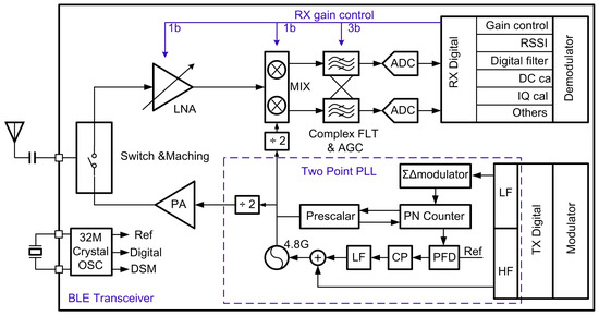
Figure 7.
The proposed BLE TRX architecture.
The RF signal passes first through the integrated TRX-switch and matching network, in which the inductor is shared between RX and TX. The on-chip switch drives the single-end variable-gain LNA, which amplifies the RX signal before it is fed to a current bleeding quadrature down conversion mixer. A 4th order complex band pass filter (BPF) follows the mixer, which performs channel selection, image rejection and anti-aliasing filtering, and also serves as a programmable gain amplifier. The IF signal is then digitized by a 3rd order delta-sigma continuous time (CT) ADC [26]. After that, the signals are further processed in the digital sections, such as additional channel select digital filtering, RSSI estimation, dc offset cancellation, automatic gain control (AGC), IQ imbalance calibration, and demodulation [27].
For BLE intermodulation characteristics, the required signal shall be measured at a power level of 6 dB over the reference sensitivity level [4]. The minimum BLE requirements for the input 3rd intermodulation point (IIP3) and input 2nd intermodulation point (IIP2) can be calculated as follows [28]. IIP3 (min) = Pin + 1/2 × (P1 − P3). Where Pin = −50 dBm, P3 = −70 (sensitivity) + 6 (dB) −14 (SNR) = −78 dBm and P1 = −50 dBm. Thus, IIP3 (min) = −36 dBm. A −22 dBm IIP2 (min) is calculated in a similar way. However, in order to increase the link margin, IIP3 above −20 dBm and IIP2 above 0 dBm was targeted in this work.
BLE TXs usually adopt two architectures: conventionally mixer-based [29], and two-point PLL-based TX [22]. The mixer-based TXs can support universal modulations, but at the expense of high circuit complexity and power consumption. Additionally, the severe PA-to-VCO coupling in mixer-based TXs [30] gives rise to frequency pulling effect, which degrades the TX modulation accuracy and increases output spectral regrowth [31,32]. In this work, the TX employed a two-point PLL-based architecture with a non-linear PA to eliminate the power-hungry RF mixers and quadrature local oscillator (LO) generators, as shown in Figure 7. High frequency (HF) and low frequency (LF) data paths are produced from digital domain to directly modulate a fractional-N synthesizer working at two times carrier frequency. LF acted as the first point modulation which can be modulated by a slowly-varying frequency modulation (FM) signal. On the other hand, HF extended the FM bandwidth to beyond the PLL bandwidth, which is the second point modulation. After dividing by 2, the modulated signal is directly fed to a nonlinear PA. Although the specified minimum output power of BLE standard is −20 dBm [4], the 0 dBm transmit power is targeted in this work.
The PLL phase noise not only affects the EVM of RX and TX, but also affects the interference and intermodulation performance. For the BLE specification [4], the interference performance shall be measured with a wanted signal 3 dB over the reference sensitivity level. The minimum BLE requirements for phase noise at offset 3 MHz can be calculated as:
where P(blocker) is the adjacent (3 MHz) interference which is 27 dB higher than the wanted signal, and 10 × log(1M) is the logarithm of 1 M transmitted bandwidth. However, in order to increase the link budget, the phase noise at offset 3 MHz was designed to below −110 dBc/Hz in this work.
PN(max)@3M = −70 dBm + 3 − 14 (SNR) − P(blocker) − 10 × log(1M) = −106 dBc/Hz
3.2. Down Conversion
Figure 8 illustrates one path of the quadrature mixer. Although the popular passive mixer [9] can save current in mixer stage, it needs large current to drive LO to full swing, and thus it is not considered in this work. Acting as a Gilbert type, this mixer employed PMOS as input and switch transistors for smaller flick noise. The dummy mixer renders the mixer symmetric from the LO standpoint and enhances IIP2. The square root currents of the input PFETs PM11 and PM12 are proportional to the mixer linearity, while the larger current, the larger LO swing is required for the switching transistors. Meanwhile, increasing the switching current will increase the switching stage noise. In order to solve the trade-offs among noise, linearity and power consumption, the current-bleeding prototype was employed in this work. To minimize the differences in the two halves caused by the single-end output of LNA, the gate of PM12 in dummy mixer is connected to a resistor R13 and capacitor C12, which matches the output impedance of the single LNA at the desired RF frequency. The resistors R11 and R12 not only act as the mixer load, but also serve as roofing filter together with capacitance C11. This filter implements the first channel filtering pole in the RX path.
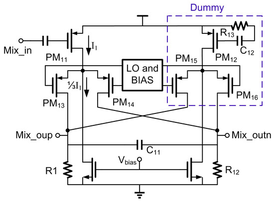
Figure 8.
Simplified schematic of down conversion.
3.3. LPF and ADC
Following the mixer, out-of-band blockers and image interferences are filtered out sufficiently by the analog baseband 4th Butterworth active-RC complex filters. This 4th order complex filter is achieved with two 2nd order filters cascaded, and the simplified schematic of the 2nd order complex filter is given in Figure 9.
Figure 9.
The simplified schematic of a 2nd order complex filter.
Compared with the real BPF, complex filter provides rejection at the image channel. In addition, the complex filters act as programmable gain amplifiers, with gain range from 2 to 20 dB controlled by the digital module. This relatively low voltage gain prevents the DC-offset saturating the coming stages even without the DC-offset cancellation circuits. Though an active-RC circuit is commonly used as the complex filter, its frequency characteristics vary with the RC time constants, which are likely to change due to power, voltage and temperature (PVT) variations. To handle this issue, RC constant time calibration circuits [33] is added in this work.
The complex filters also provide anti-alias filtering for the 3rd order delta-sigma CT ADC, which is sampled with a 128 MHz clock. The simulated magnitude-frequency response of the 4th order complex filter is shown in Figure 10, that more than 150 dB attenuation at 128 MHz is obtained, which avoid aliasing issue. The CT-ADC loop coefficients employ active-RC networks and can be digitally tuned using the same code generated by the RC constant time calibration circuits in complex filter.
Figure 10.
The simulated magnitude-frequency response of the 4th order complex filter.
3.4. Synthesizer
As shown in Figure 7, the LO is generated by a 4.8 GHz fractional-N synthesizer [34], consisting of a phase-frequency detector (PFD), a charge pump (CP) current source, a loop filter, a third order multi-stage noise shaping (MASH) delta-sigma modulator (DSM), a dual-modulus prescaler, programmable dividers, and a voltage-controlled oscillator (VCO). Considering the phase noise and respond time, the PLL loop bandwidth of 120 kHz was adopted in this work. However, this loop bandwidth is significantly smaller than the BLE specified 1 Mb/s rate with GFSK modulation. To extend the modulation bandwidth, a two-point modulation scheme is applied to reuse the synthesizer. This simultaneously guarantees reduced noise performance in both TX and RX modes.
Figure 11 shows the simplified VCO schematic. The NMOS only cross-coupled topology is employed due to its better phase noise performance [35] in low power design. The charge pump output is applied to MOS-varactors C22 and C23 for fine frequency and phase-locking after the 3-order loop filter. To improve the linearity of the VCO gain (Kvco), both C22 and C23 were designed to have two combined varactors biased to ground. An 8 bit DAC is added as HF (the second point) to extend the frequency modulation bandwidth beyond the PLL bandwidth. The designed frequency resolution is about 2 kHz. A symmetric and differential customized inductor is adopted to increase the Q-value and reduce current consumption. Current biasing is achieved by a variable poly resistor R21, which suffers lower noise as comparing to a tail current source. The output impedance of NM21 and NM22 are increased through NM23 and NM24 by using negative feedback, which makes the node (VF) voltage be less sensitive to external interference and provide steadier current for resonance device. Therefore, the phase noise of the VCO is much less sensitive to bias noise in low frequencies [23].
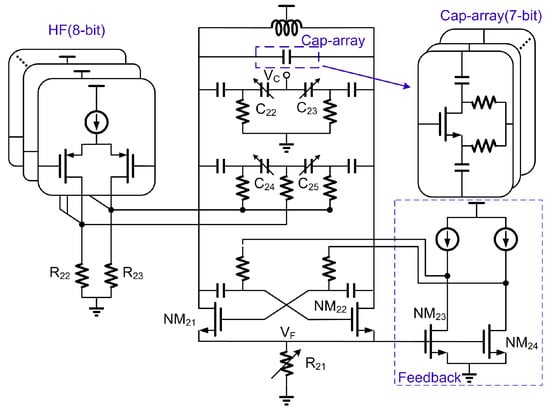
Figure 11.
Simplified schematic of VCO.
To cover frequency range from 4.8 GHz to 4.967 GHz (two times of ISM band frequency), a 7-bit capacitor array was used as shown in Figure 11. In order to speed up the lock time, initial coarse frequency algorithm is implemented in digital domain during startup period. The control word of the capacitor array is scanned and the corresponding frequency is calculated and stored. When channel switching, the required control word will be automatically picked up to achieve a fast lock. After the PLL has settled to the channel frequency, the HF data is then applied to other MOS varactors consisting of C24 and C25 in TX mode.
4. Measurement Results and Discussion
The BLE transceiver is implemented in a standard 110 nm CMOS technology using a single-poly and six-metal layers (one thick copper and one thick aluminum layer). The chip microphotograph is shown in Figure 12. Only two inductors, one for front-end and one for VCO, were implemented. The die area is 3.6 mm2, in which the front-end circuits only occupies 0.24 mm2 , while the rest is PLL, analog baseband, digital modular, demodulator and digital signal processing. Without using off-chip TRX-switch and Balun, this transceiver achieves small area and high-level integration.
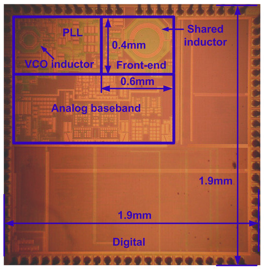
Figure 12.
Chip micrograph of the proposed BLE transceiver.
Figure 13 shows the S11 of the RX and TX. Both TX and RX achieve S11 less than 10 dB over the entire operating band. This verifies the effectiveness of the proposed TRX-switch and matching network combination scheme. The discrepancy between the measured S11 and simulated S11 (shown in Figure 4 and Figure 6) might result from the inaccurate modeling from both inductor and the parasitic components of PCB and bonding wire.
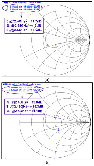
Figure 13.
(a) Measured TX impedance in SMITH chart; (b) Measured RX impedance in SMITH chart from 2.4 GHz to 2.5 GHz.
The noise performance of the RX has been evaluated from the antenna port to the ADC outputs. Figure 14 shows the measured RX performance. The NF of the RX shown in Figure 14a achieves 6–7 dB within the ISM band. Therefore, the sensitivity for the BLE Standard calculated from (1) is about −93 dBm, which is much higher than the BLE specification requirements (−70 dBm). The total current consumption of RX is 9.7 mW, and the power loss breakdown of RX is shown in Figure 14b. Among the RX power losses, the ADC and complex filter consume 2.4 and 1.4 mW, respectively, which are mainly from their operational amplifiers. LNA consumes 1 mW, 70% of which is from the first stage, while the buffer contributes the remaining 30%. The mixer consumes less than 0.5 mW which is mainly from the core circuits. 1 mW is consumed by BBPLL, 40% of which is from the ring oscillator, 20% from PFD, 20% from CP, the rest from divider. RFPLL consume about 2.1 mW of power, with its VCO, PFD, CP and prescalar consuming 1 mW, 0.2 mW, 0.2 mW and 0.6 mW, respectively.
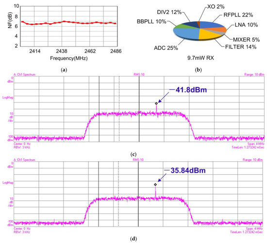
Figure 14.
(a) Measured NF in ISM band; (b) RX power loss breakdown; (c) Measured the third-order intermodulation product; (d) Measured the two-order intermodulation product.
For the linearity performance, the measured 1 dB compression point (P1dB) of the receiver is about −29 dBm. Additionally, Figure 14c,d show the 3rd and 2nd intermodulation products. Two interfering sine wave signals (listed in Table 1) are input to the receiver with a channel gain GC = 74 dB, and IIP3 = Pin + (Pin + GC − PO3)/2, while IIP2 = 2Pin − PO2 + GC. The measured IIP3 and IIP2 are thus −17.1 dBm and 9.8 dBm. The IIP2 performance might result from the following factors: (1) The single-ended LNA used in this work does not suppress the even-order harmonic distortion; (2) The input of down-mixer is not exactly symmetrical, as shown in Figure 8, which causes the even-order harmonic rejection not as good as a fully differential topology. But the IIP2 performance of this work still meets the intermodulation requirement in BLE standard [4]. For the more severe cases not defined in [4], such as that with a large modulated out-of-band interference, a SAW filter might be needed for this work.

Table 1.
IIP3 and IIP2 measurement conditions and results.
Figure 15a shows that the TX output power variations are less than 1 dB within the 2.4 GHz ISM band. The TX current consumption for various output powers is plotted in Figure 15b. It consumes 9.4, 8.4 and 7.9 mW at output powers of 0, −3 and −10 dBm, respectively. Figure 16a shows the measured eye diagram and spectrum of BLE modulation (BT = 0.5), and Figure 16b gives the in-band spurious emission performance, which is far less than the requirement in the dashed lines. The measured FSK error of BLE is 2.97% as shown in Figure 16c. All the measured modulations meet the accuracy specifications with decent margins. The power loss breakdown of TX with 0 dBm output is shown in Figure 16d. Most of the power loss is from PA, which is 5.8 mW. The last stage of the PA contributes more than 80% of this power consumption. On the other hand, the power loss on the PLL, XO and divider-by-2 circuit are similar to those in the receiver. The PA efficiency is not as high as the state-of-art works due to the following two reasons: (1) The cascode stage of PA (NM3) employs thick gate oxide to ensure the reliability of PA. However, the on-resistance and parasitic capacitance of thick gate oxide FET are larger than the thin gate oxide FET. Therefore, more power is consumed, comparing to the scheme using thin gate oxide FET; (2) This work employed an 110 nm CMOS process. With much larger parasitic capacitance, the switching loss is larger for this design.
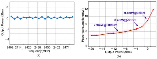
Figure 15.
(a) Measured Pout variation VS ISM band frequency; (b) Measured power consumption vs. output power.
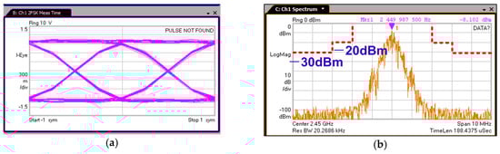
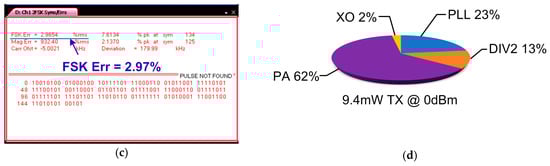
Figure 16.
Measured TX performance. (a) Measured eye diagram of BLE (BT = 0.5); (b) Measured spectrum of BLE; (c) Measured FSK Error; (d) Power consumption summary at 0 dBm output power.
The measured output spectrum is presented in Figure 17, with 0 dBm required signal and −34.82 dBm 2nd harmonic emission, which meets the specification of the European standard [36] Considering the out-of-band spurious emission requirements are different in the intended countries of sales [4], more severe requirements in other standards might be employed for some specific applications. In this scenario, this design should further reject the 2nd harmonic by using a SAW filter, or reducing the output power.
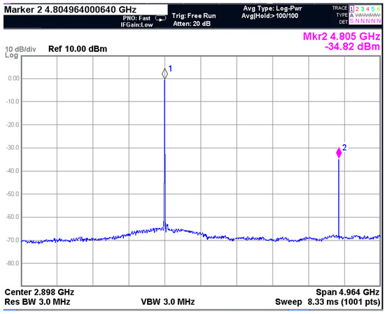
Figure 17.
The measured output spectrum with 0 dBm required signal and −34.82 dBm 2nd harmonic spurious emission.
The PLL phase noise is measured at the VCO output and the result is ploted in Figure 18a. At 4.8 GHz, the phase noises at 10 kHz, 1 MHz and 3 MHz offsets are −83 dBc/Hz, −108 dBc/Hz and −114 dBc/Hz, respectively. When applied to the LO port, the phase noise will be reduced by 6 dB due to the VCO frequency divided by 2. Therefore, the phase noise in this work is far lower than the BLE system requirements. As shown in Figure 18b, the measured PLL lock time is faster than 33 μs.
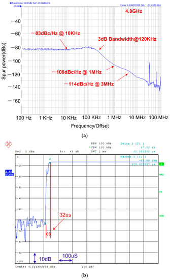
Figure 18.
(a) Measured PLL phase noise at 4.8 GHz; (b) Measured PLL lock time.
The performance of the proposed transceiver is summarized and compared with some state-of-the-art designs in Table 2. Due to the proposed front-end, only two inductors were employed in this work, and a minimum front-end silicon area is achieved. Furthermore, the TRX-switch and matching network are integrated in this work. By optimizing the impedance and matching network, and choosing a single-ended architecture for both LNA and PA, comparable S11, NF, output power and linearity are achieved with this proposed design. These verify the effectiveness and applicability of the proposed BLE transceiver for WSNs applications.
Table 2.
Comparison to the state-of-art works.
5. Conclusions
A 2.4 GHz ISM band, low cost BLE transceiver for WSNs application with RX matching network reusing PA load inductor in front-end is fabricated in a 0.11 μm CMOS technology. RX achieves a sensitivity of −93 dBm for BLE and consumes 9.7 mW. For TX, it achieves a 2.97% BLE FSK error and consumes 9.4 mW at 0 dBm output power. The front-end circuit occupies approximately 0.24 mm2. Measurement results verify the effectiveness and applicability of the proposed BLE transceiver for WSN applications.
Acknowledgments
This work was financially supported by the three grants from Natural Science Foundation of China (61604044) and (61571196), and Science and Technology Program of Guangzhou, China (201604010030).
Author Contributions
Zhen Liang, Bin Li and Mo Huang conceived the idea, designed and measured this chip, and wrote the paper. Yanqi Zheng, Fangming Deng, Hui Ye and Ken Xu co-designed and measured this chip, and revised the paper.
Conflicts of Interest
The authors declare no conflict of interest.
References
- Abbas, Z.; Yoon, W. A Survey on Energy Conserving Mechanisms for the Internet of Things: Wireless Networking Aspects. Sensors 2015, 15, 24818–24847. [Google Scholar] [CrossRef] [PubMed]
- Cerruela, G.G.; Luque, R.I.; Gómeznieto, M.Á. State of the Art, Trends and Future of Bluetooth Low Energy, Near Field Communication and Visible Light Communication in the Development of Smart Cities. Sensors 2016, 16, 1968. [Google Scholar] [CrossRef] [PubMed]
- Aguilar, S.; Vidal, R.; Gomez, C. Opportunistic Sensor Data Collection with Bluetooth Low Energy. Sensors 2017, 17, 159. [Google Scholar] [CrossRef] [PubMed]
- Bluetooth, S.I.G. Bluetooth Specification, Version 4.2. Available online: https://www.bluetooth.org/en-us/specification/adopted-specifications (accessed on 18 April 2017).
- Eldesouki, M.M.; Qasim, S.M.; Bensaleh, M.S.; Deen, M.J. Toward Realization of 2.4 GHz Balunless Narrowband Receiver Front-End for Short Range Wireless Applications. Sensors 2015, 15, 10791–10805. [Google Scholar] [CrossRef] [PubMed]
- Nguyen, T.K.; Krizhanovskii, V.; Lee, J.; Han, S.K. A Low-Power RF Direct-Conversion Receiver/Transmitter for 2.4-GHz-Band IEEE 802.15.4 Standard in 0.18-μm, CMOS Technology. IEEE Trans. Microw. Theory Tech. 2006, 54, 4062–4071. [Google Scholar] [CrossRef]
- Weber, D.; Si, W.; Abdollahi-Alibeik, S.; Lee, M.L. A Single-Chip CMOS Radio SoC for v2.1 Bluetooth Applications. In Proceedings of the IEEE International Solid-State Circuits Conference, San Francisco, CA, USA, 3–7 February 2008; pp. 364–620. [Google Scholar]
- Mekanand, P.; Prawatrungruang, P.; Eungdamrong, D. 0.5 μ CMOS 2.4 GHz RF-switch for wireless communications. In Proceedings of the IEEE International Conference on Advanced Communication Technology, Gangwon-Do, Korea, 17–18 February 2008; pp. 447–450. [Google Scholar]
- Tan, C.G.; Song, F.; Zheng, R.; Cui, J. An Ultra-Low-Cost High-Performance Bluetooth SoC in 0.11-um CMOS. IEEE J. Solid State Circuits 2012, 47, 2665–2677. [Google Scholar] [CrossRef]
- Si, W.; Weber, D.; Abdollahi-Alibeik, S.; Lee, M.L. A Single-Chip CMOS Bluetooth v2.1 Radio SoC. IEEE J. Solid State Circuits 2008, 43, 2896–2904. [Google Scholar] [CrossRef]
- Marholev, B.; Pan, M.; Chien, E.; Zhang, L. A Single-Chip Bluetooth EDR Device in 0.13 μm CMOS. In Proceedings of the IEEE International Solid-State Circuits Conference, San Francisco, CA, USA, 11–15 February 2007; pp. 558–759. [Google Scholar]
- Kuo, F.W.; Ferreira, S.B.; Babaie, M.; Chen, R.; Cho, L. A Bluetooth low-energy (BLE) transceiver with TX/RX switchable on-chip matching network, 2.75 mW high-IF discrete-time receiver, and 3.6mW all-digital transmitter. In Proceedings of the IEEE Symposium on VLSI Circuits, Honolulu, HI, USA, 15–17 June 2016; pp. 1–2. [Google Scholar]
- Fu, C.T.; Lakdawala, H.; Taylor, S.S.; Soumyanath, K. A 2.5 GHz 32 nm 0.35 mm2 3.5 dB NF −5 dBm P1 dB fully differential CMOS push-pull LNA with integrated 34 dBm T/R switch and ESD protection. In Proceedings of the IEEE International Solid-State Circuits Conference, San Francisco, CA, USA, 20–24 February 2011; pp. 56–58. [Google Scholar]
- Liu, X.; Mok, P.K.T.; Jiang, J.; Ki, W.H. Analysis and Design Considerations of Integrated 3-Level Buck Converters. IEEE Trans. Circuits Syst. I Regul. Pap. 2016, 63, 671–682. [Google Scholar] [CrossRef]
- Liu, X.; Huang, C.; Mok, P.K.T. A 50 MHz 5 V 3 W 90% efficiency 3-level buck converter with real-time calibration and wide output range for fast-DVS in 65 nm CMOS. In Proceedings of the IEEE Symposium on VLSI Circuits (VLSIC), Honolulu, HI, USA, 15–17 June 2016; pp. 1–2. [Google Scholar]
- Liu, X.; Zhang, H. A 2.4 V 23.9 dBm 35.7%-PAE-32.1 dBc-ACLR LTE-20MHz Envelope-Shaping-and-Tracking System with a Multiloop-Controlled AC-Coupling Supply Modulator and a Mode-Switching PA. In Proceedings of the IEEE International Solid-State Circuits Conference, San Francisco, CA, USA, 5–9 February 2017; pp. 38–39. [Google Scholar]
- Taris, T.; Mabrouki, A.; Kraimia, H.; Deval, Y. Reconfigurable Ultra Low Power LNA for 2.4 GHz Wireless Sensor Networks. In Proceedings of the IEEE International Conference on Electronics, Circuits, and Systems, Athens, Greece, 12–15 December 2010; pp. 74–77. [Google Scholar]
- Song, T.; Oh, H.S.; Yoon, E.; Hong, S. A low-power 2.4-GHz current-reused receiver front-end and frequency source for wireless sensor network. IEEE J. Solid State Circuits 2007, 42, 1012–1022. [Google Scholar] [CrossRef]
- Chen, M.; Wang, K.H.; Zhao, D.; Dai, L. A CMOS Bluetooth radio transceiver using a sliding-IF architecture. In Proceedings of the IEEE Custom Integrated Circuits Conference, San Jose, CA, USA, 21–24 September 2003; pp. 455–458. [Google Scholar]
- Zhang, L.; Jiang, H.; Wei, J.; Dong, J. A reconfigurable sliding-if transceiver for 400 MHz/2.4 GHz IEEE 802.15.6/ZigBee WBAN hubs with only 21% tuning range VCO. IEEE J. Solid State Circuits 2013, 48, 2705–2716. [Google Scholar] [CrossRef]
- Liu, Y.H.; Ba, A.; Van den Heuvel, J.H.C.; Philips, K. A 1.2 nJ/bit 2.4 GHz Receiver with a Sliding-IF Phase-to-Digital Converter for Wireless Personal/Body Area Networks. IEEE J. Solid State Circuits 2014, 49, 3005–3017. [Google Scholar] [CrossRef]
- Masuch, J.; Delgado-Restituto, M. A 1.1-mW-RX, -dBm Sensitivity CMOS Transceiver for Bluetooth Low Energy. IEEE Trans. Microw. Theory Tech. 2013, 61, 1660–1673. [Google Scholar] [CrossRef]
- Gil, J.; Kim, J.H.; Kim, C.S.; Park, C. A Fully Integrated Low-Power High-Coexistence 2.4-GHz ZigBee Transceiver for Biomedical and Healthcare Applications. IEEE Trans. Microw. Theory Tech. 2014, 62, 1879–1889. [Google Scholar] [CrossRef]
- Liu, Y.H.; Bachmann, C.; Wang, X.; Zhang, Y. A 3.7mW-RX 4.4 mW-TX fully integrated Bluetooth Low-Energy/IEEE802.15.4/proprietary SoC with an ADPLL-based fast frequency offset compensation in 40 nm CMOS. In Proceedings of the IEEE International Solid-State Circuits Conference, San Francisco, CA, USA, 22–26 February 2015; Volume 13, pp. 1–3. [Google Scholar]
- Sano, T.; Mizokami, M.; Matsui, H.; Ueda, K. A 6.3mW BLE transceiver embedded RX image-rejection filter and TX harmonic-suppression filter reusing on-chip matching network. In Proceedings of the IEEE International Solid-State Circuits Conference, San Francisco, CA, USA, 22–26 February 2015; Volume 13, pp. 1–3. [Google Scholar]
- Huang, M.; Chen, D.H.; Wang, Z.; Guo, J.; Dagher, E.H. A power-area-efficient, 3-band, 2-RX MIMO, TD-LTE receiver with direct-coupled ADC. Int. J. Circuit Theory Appl. 2015, 43, 806–821. [Google Scholar] [CrossRef]
- Retz, G.; Shanan, H.; Mulvaney, K.; O’Mahony, S. A highly integrated low-power 2.4 GHz transceiver using a direct-conversion diversity receiver in 0.18 µm CMOS for IEEE 802.15.4 WPAN. In Proceedings of the IEEE International Solid-State Circuits Conference, San Francisco, CA, USA, 8–12 February 2009; pp. 414–415. [Google Scholar]
- Pipino, A.; Liscidini, A.; Wan, K.; Baschirotto, A. Bluetooth low energy receiver system design. In Proceedings of the IEEE International Symposium on Circuits and Systems, Lisbon, Portugal, 24–27 May 2015; pp. 465–468. [Google Scholar]
- Kwon, Y.I.; Park, S.G.; Park, T.J.; Cho, K.S. An Ultra Low-Power CMOS Transceiver Using Various Low-Power Techniques for LR-WPAN Applications. IEEE Trans. Circuits Syst. I Regul. Pap. 2012, 59, 324–336. [Google Scholar] [CrossRef]
- Huang, M.; Chen, D.H.; Guo, J.P.; Xu, K. A tri-band, 2-RX MIMO, 1-TX TD-LTE CMOS transceiver. Microelectron. J. 2015, 46, 59–66. [Google Scholar] [CrossRef]
- Razavi, B. A study of injection locking and pulling in oscillators. IEEE Int. J. Solid State Circuits 2004, 39, 1415–1424. [Google Scholar] [CrossRef]
- Hsiao, C.H.; Li, C.J.; Wang, F.K.; Horng, T.S. Analysis and Improvement of Direct-Conversion Transmitter Pulling Effects in Constant Envelope Modulation Systems. IEEE Trans. Microw. Theory Tech. 2012, 58, 4137–4146. [Google Scholar] [CrossRef]
- Huang, M.; Chen, D.; Guo, J.; Ye, H. A CMOS Delta-Sigma PLL Transmitter with Efficient Modulation Bandwidth Calibration. IEEE Trans. Circuits Syst. I Regul. Pap. 2015, 62, 1716–1725. [Google Scholar]
- Prummel, J.; Papamichail, M.; Willms, J.; Todi, R. A 10 mW Bluetooth Low-Energy Transceiver with On-Chip Matching. IEEE Int. J. Solid State Circuits 2015, 50, 3077–3088. [Google Scholar]
- Babaie, M.; Kuo, F.W.; Chen, H.N.R.; Cho, L.C. A Fully Integrated Bluetooth Low-Energy Transmitter in 28 nm CMOS with 36% System Efficiency at 3 dBm. IEEE J. Solid State Circuits 2016, 51, 1–19. [Google Scholar] [CrossRef]
- ETSI. EN 300 328 V1.8.1. Available online: http://www.etsi.org/deliver/etsi_en/300300_300399/300328/01.08.01_60/en_300328v010801p.pdf (accessed on 18 April 2017).
- nRF8001 Preliminary Product Specification. Available online: https://wenku.baidu.com/view/6fc358c02cc58bd63186bdb5.html (accessed on 18 April 2017).
© 2017 by the authors. Licensee MDPI, Basel, Switzerland. This article is an open access article distributed under the terms and conditions of the Creative Commons Attribution (CC BY) license (http://creativecommons.org/licenses/by/4.0/).