4.1. Effects of the Excess Carrier Photo-Generation, Recombination and Surface Charging
In these experiments excitation quanta of less energy (
Eph = 3.50 eV and 2.33 eV) than the forbidden energy-gap in diamond (
EG = 5.46 eV) were used. Thereby, the excess carrier domains can be generated either by non-linear absorption or via photo-ionization of filled deep traps. Therefore, for separation of prevailing mechanisms of photo-excitation, it is important to clarify whether the monopolar or bipolar (as carrier pair) initial generation is implemented. The non-linear absorption processes of two-photon via virtual states or two-step absorption through empty deep levels are most probable processes. It had been proved [
35] that both two-photon and two-step processes compete in generation of excess carrier pairs in defect-rich HPHT diamond samples at elevated excitation intensities. It was revealed that photo-ionization of filled deep traps can be performed by 2.33 eV quanta in defect-rich HPHT diamond samples [
35]. This leads to a nearly linear dependence of the optical transmission signal on excitation intensity. The carrier pair generation has been implied from these measurements where electrons are generated from donor type deep traps while holes appear in valence band through rapid capture of electrons from valence band to the photo-emptied traps of large density.
Optical transmission of the
d thickness wafer sample can be described by a function:
of the excitation power density
Pex and of the coefficients of the linear absorption α, of the two-photon absorption β and of the two-step absorption β
S if all the mentioned photo-excitation processes appear simultaneously. In spectral range of sample transparency (for α
d << 1 and α
d < (β+ β
S)
Pexd), this expression can be simplified as:
Then carrier excitation rate is related to the absorption and laser pulse parameters as:
The concentration generated at the end of a laser pulse τ
L (in the case of fast recombination τ
L ≤ τ
R) is evaluated by the convolution integral averaged over laser pulse duration τ
L expressed as:
here,
b is a dimensionless parameter characterizing a temporal width of Gaussian laser pulse. It has been obtained that
n0(
t = 0) varies as a function of excitation intensity
I0: for HPHT samples, as
n0(
t = 0)~I0 for the range of a threshold
I0 values sufficient to detect current transients. While it becomes
n0(t = 0)
~I02 for HPHT sensors at elevated excitation intensities. For the CVD diamond samples, the
n0(
t = 0)
~I02 characteristic prevails over the entire range where current transient signals can be detected. This implies a higher CVD crystal quality corroborated by the significantly longer carrier lifetimes in this material relative to the tested HPHT diamond samples. On the other hand, the concentration of the electrically active defects, attributed to the residual metals and nitrogen in the HPHT diamond material [
35], exceeds that of CVD diamond [
37] by more than four orders of magnitude. Additionally, owing to the longer carrier lifetime in CVD diamond, the peak amplitude of the initial component of the current pulse has been examined as a function of excitation intensity keeping a fixed value
U of applied voltage to capacitor type detector (
Figure 7). As can be deduced from Equations (3) and (10), the current peak value
i1,peak is proportional to ~(
Sεε0U/2
dψ
)τ
Mn0−1 ≈ (
Sεε0U/2
Xe0)τ
Mn0−1 = (
eμ
eSU/Xe0)
n0 and
Xe0~n0−1,
i.e.,
i1,peak~n02.
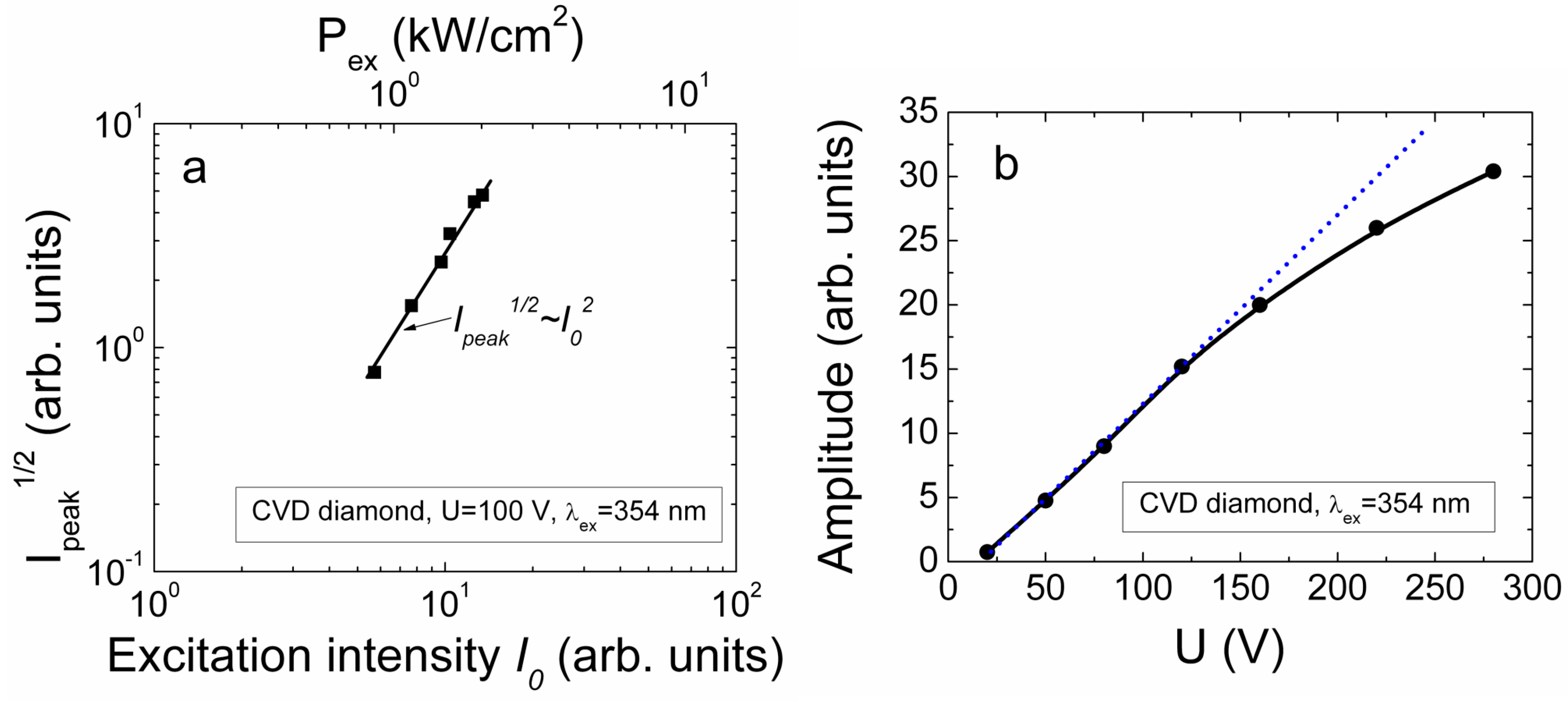
Figure 7.
(a) The current peak amplitude as a function of excitation intensity at fixed value of applied voltage. The top scale indicates the range of applied power densities; (b) The current peak amplitude as a function of applied voltage for the fixed excitation intensity. Both characteristics were measured for CVD diamond by using injection of bulk domain with UV excitation wavelength λex = 354 nm.
The measured dependence of
i1,peak on excitation intensity (for CVD diamond detector of capacitor type with injected bulk domain) is presented in
Figure 7a. This dependence corroborates
n0(
t = 0)
~I02,
i.e., the excess carrier generation through the two-photon absorption dominates in CVD diamond. The range of the excitation power densities
Pex (upper scale on
Figure 7a) from the side of low values is there limited by sensitivity of the measurement system to record current signals. Due to steep increase of the current peak values (
Ipeak~Pex4~I04) and necessity to keep the linearity of electrode characteristics, the dynamic range for
Pex is also limited from the top side. Additionally, the upper range for values of the excitation power densities
Pex can be shifted by using laser beam focusing. However, surface damage of diamond wafers can easily be reached (especially for HPHT samples).
The signal dependence on applied voltage for the fixed excitation intensity appears to be a linear function (
Figure 7b) over a wide range of voltages. This can be explained by a relation
i1,peak~(
Sεε0U/2
Xe0)τ
Mn0−1~U. However, the change of the current enhancement slope with applied voltage within
i1,peak~f(U) characteristic can be observed in
Figure 7b, at the highest voltages exploited. This effect of
i1,peak~f(U) slope change (similar to a current saturation effect) can be explained by competition of voltage dependent changes of
i1,peak~U/
Xe0 (Equations (4) and (5)) and of
Xe0~U (Equation (3)). This effect is also similar to a change of an I-V characteristic going from partial depletion regime to that of above full depletion voltage regime, within junction structures. Thereby, the saturation effect is determined by the significant separation of the injected sub-domains by the external voltage caused electric field.
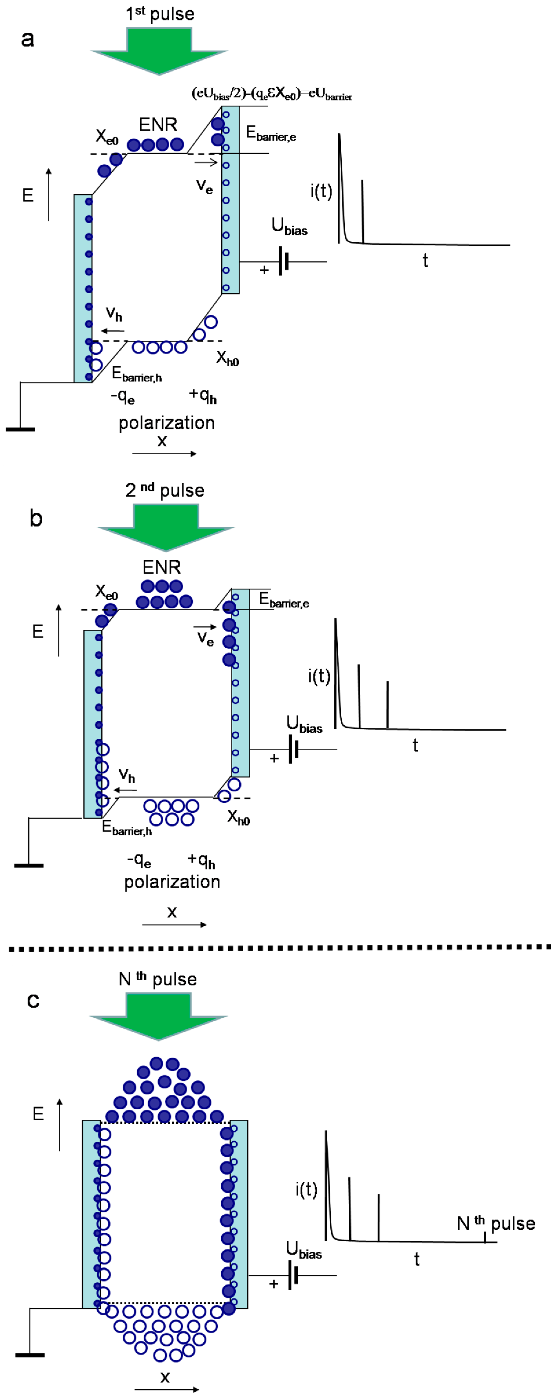
A polarization effect, similar to that reported in [
13,
16,
28,
29,
30,
31], has been unveiled in diamond samples. This effect (
Figure 8a and
Figure 9) appears as a decrease of the current peak amplitudes under action of a set of light pulses with invariable switched-on DC voltage. Actually the current signal nearly disappears using the same injection conditions if a capacitor type detector is kept with unipolar applied voltage of moderate values for a long exposure to a set of the injection light pulses with rather high repetition rate.
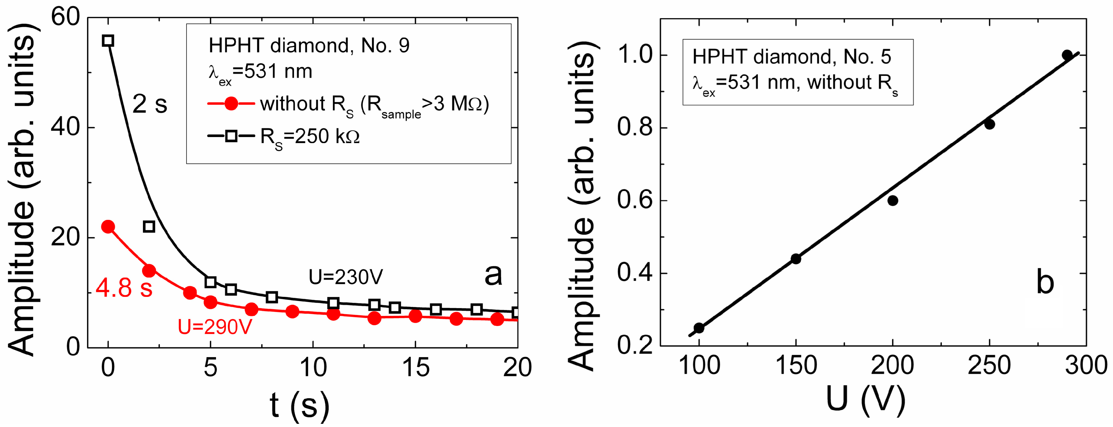
Figure 8.
(a) Evolution of the current peak amplitude just after sharp switch-on a voltage of 290 V without (solid symbols) and with (hollow symbols) shunt resistance, measured in capacitor type detector made of HPHT diamond; (b) The current peak amplitude as a function of applied voltage for the fixed excitation intensity. These characteristics were measured by using injection of bulk domain at excitation wavelength λex= 531 nm.
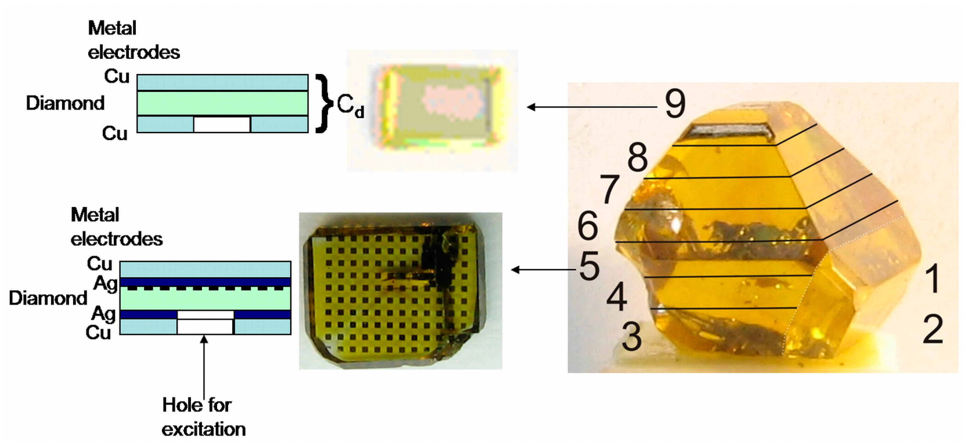
This polarization effect appeared to be independent of conditions of capacitor formation on diamond samples—the same phenomenon was inherent for both the mosaic electrode system containing sample No. 5 of the HPHT wafer set and the two-component metallization as well as the single copper metal, pressed electrodes on samples No. 7 and No. 9 [
35] (
Figure 1 and
Figure 2). The polarization effect was observed for all the investigated HPHT and CVD diamond samples, being a little bit stronger for HPHT samples. This effect can be slightly suppressed by increasing of the applied voltage value. Therefore, evolution of the current peak amplitudes in profiling measurements has been examined just after a sharp voltage switch-on,
i.e., ascribed to a single light pulse, to keep nearly the same acting electric field. The recovery of the acting electric field can be implemented either by a short-circuiting of the device electrodes or by applying the opposite polarity voltage. In the latter case, the capacitor charging current pulse of the opposite polarity is inevitably observed. Therefore, examination of the drift current transients is preferential at elevated applied voltages of moderate and large values, in order to reduce the role of the polarization effect.
Figure 9.
(a) A sequence of the charging current amplitudes (right scale) for a 700 ms pulse of the unipolar bias (16 V) voltage (left scale) applied to CVD diamond. The solid (red) curve is an eye-guide which shows the charging current decrease after each laser pulse of duration 0.4 ns in sequence of 70 laser pulses; (b) A sequence of the charging current amplitudes (right scale) for the 70 ms voltage pulses of the bipolar ± 14 V bias voltage (left scale) applied on CVD diamond capacitor. The solid (red) curve is again an eye-guide which shows the charging current (as vertical lines in this display scale) reduction after each laser pulse of duration 0.4 ns in sequence of 7 laser pulses (with 100 Hz repetition rate) for the negative and the positive polarity of bias voltage, respectively.
The recorded evolution of the current peak amplitude in HPHT diamond structure just after a sharp switch-on of the moderate values of the applied voltage is illustrated in
Figure 8a for 531 nm excitation wavelength. However, this effect was found for both 531 and 354 nm excitation wavelengths. The nearly linear dependence of the current peak amplitudes on the applied voltage have been obtained for the HPHT diamond detectors (
Figure 8b). This characteristic proves the non-injecting electrodes over the range of applied voltages and of densities of the injected excess carriers. Therefore, the carrier trapping/recombination component has been hypothesized within induction currents in HPHT diamond samples. The linear excess carrier excitation regime can also be implied from these characteristics,
Figure 8b. Then, formation of current transients can be described by the additional, carrier trapping component in Equation (17). In the reported approaches (e.g., [
16]), the polarization effect is exceptionally interpreted assuming only this carrier trapping/de-trapping current component caused by non-movable space charge formation. Rapid trapping of the excess carriers onto deep centres can lead to the formation of the localized non-movable charge within
Xe0 region. This localized charge in
Xe0 keeps the induced charge Δσ at electrode till then the excess carriers are thermally/optically de-trapped from the deep centres to conduction/valence bands. The long de-trapping time from these deep centres can be a reason for a rather long relaxation (
Figure 8a) of the quasi-stationary polarization field. Such characteristics and their interpretation are compatible with reported results and model in [
16]. To verify whether this polarization appears due to bulk localized charge within
Xe0 or via charge induction at electrode, the bypassing circuit was employed using a shunt resistance (
Figure 2a) connected in parallel to the device under test.
The shunt resistance was chosen to be large enough in order to keep nearly the same voltage drop on the inter-electrode gap, while the shunt resistance value was significantly less than that of the diamond sample. Verification of polarization was based on possibility to drain the induced charge Δσ from electrodes through shunt resistance, which is tunable to change the bulk localized charge within
Xe0 till then the de-trapped carriers are brought from the
Xe0 by their drift. The cumulated charge on electrodes can additionally be a reason for shielding of the external voltage source field. These measurements showed (
Figure 8a, upper curve) that the current signal really increases and relaxation becomes faster, if shunt resistance is connected, relative to that without bypass circuit when other experimental conditions are kept the same. Thereby, it can be tentatively assumed that the polarization effect is caused by a cumulating of the induction charge on electrodes due to excess carrier localization at deep centres. Then, the space charge within widths
Xe0,
Xh0 can appear due to charging of deep traps by captured excess carriers. This bulk localized charge determines the slow component of recharging through excess carrier de-trapping.
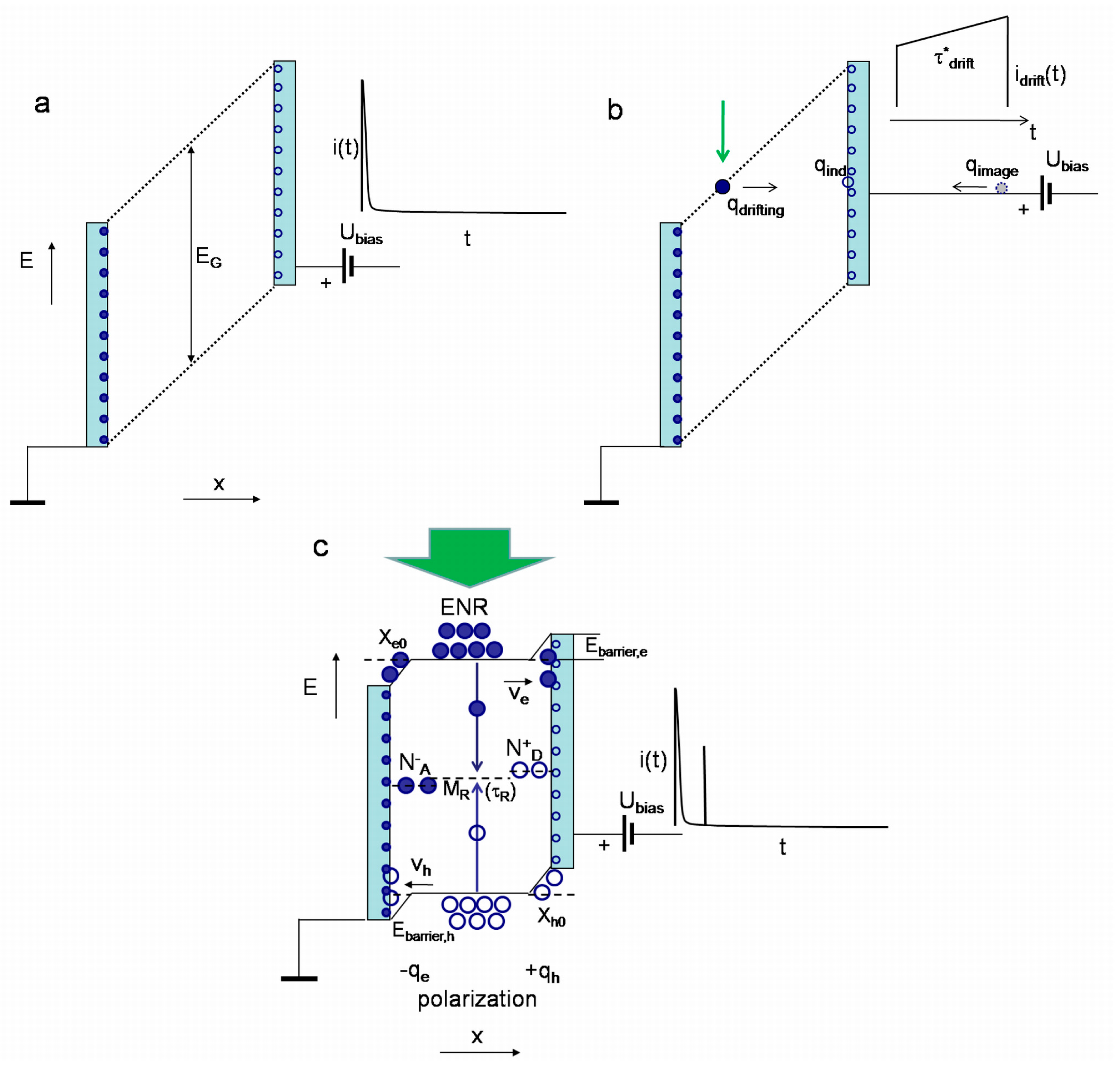
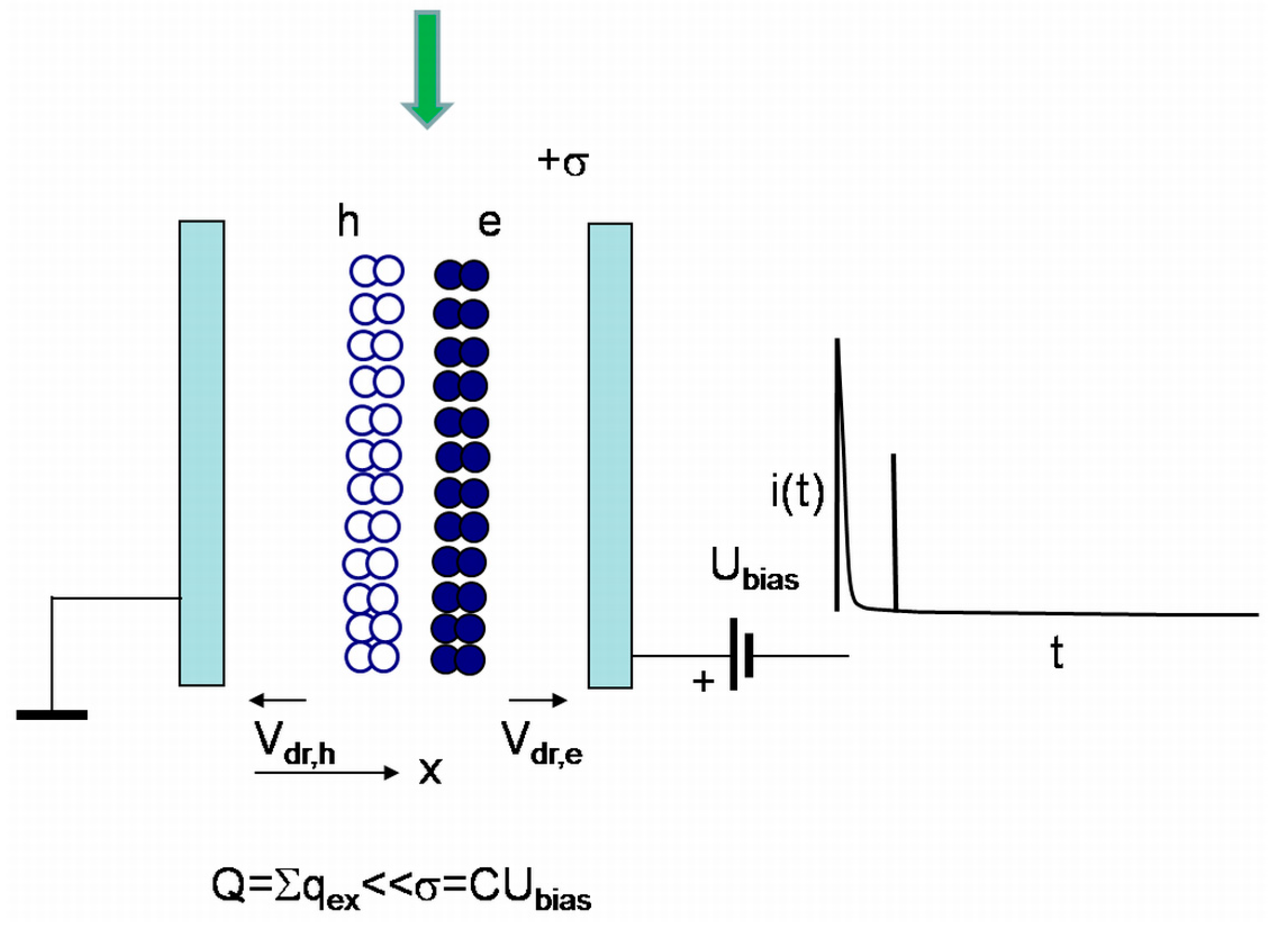
These observations prove a hypothesis of the induced charge Δσ on the electrodes and its accelerated extraction by partial shunting. These changes of relaxation rate also imply a dynamic component of the polarization effect attributed to free excess carriers (
Figure 3c and
Figure 4). A current transient, originated from a single light pulse through induction of surface charges at electrodes, may contain two components (Equation (16)) for each type of excess carriers: caused by the excess carrier drift and by the changes in time of the excess charge amount via carrier capturing into deep traps. As a result, the extracted charge at electrode appears (through fast drift component) which prevents further extraction of the same type carriers. Really, the external battery determines flow of currents by balancing the induction charges, to keep invariable external voltage. In consequence of surface and bulk charges, the internal electric fields appear, those are able to compensate the external source determined field. Thereby, the resulting electric field, acting on excess carriers, changes under cumulated excess carriers, if repetition rate of the injection light pulses is high in comparison with dielectric relaxation rate (
Figure 8a). The polarization effect can alternatively be explained (
Figure 4) by free carriers accumulated within regions of electrodes (polarity of which, for instance, positively charged contact for excess holes prevents extraction of free non-equilibrium holes to electrode) and separated by electrically neutral region at low applied voltages. This hypothesis seems to be supported by the existence of the polarization effect irrespective of the significant difference in concentration of deep traps in HPHT and CVD diamond, due to the fact the electrically active impurities (e.g., concentration of nitrogen (N) in HPHT diamond is of about 2 × 10
19 cm
−3 while it is less by a few orders of magnitude in CVD diamond) those would be the reason for the localized bulk charge. Recombination of accumulated excess carriers in the region between the electrically neutral region (ENR) and the electrodes is prevented due to a lack of the annihilation counter-partners (for instance, excess electrons are always extracted by external field at positively charged electrode while excess holes are accumulated). The capacitor charging current (determined by the external battery) can then be reduced (after each injection light pulse) by increase of
Xe0 and
Xh0 (
Figure 4 and
Figure 9), where internal voltage compensates the battery’s voltage (more and more after each pulse within a set of laser pulses). The sequenced generation of additional excess carriers with rather high rate of laser pulse repetition might then cause a cumulating of the induced charge Δσ at electrode. It also allows us to understand why the polarization effect is independent of surface metallization of the same set of samples, as the induced charge Δσ at electrode is not caused by ions collected on surface from atmosphere and from surface traps, as well. Thus, recovery of the applied field is only possible by reversing polarity of the external battery (when surface charges cumulated at electrodes are rapidly extracted from electrodes).
To clarify the dynamic component of polarisation field, experiments with pulsed external voltage source have been performed using a scheme shown in
Figure 2c. There either a unipolar voltage pulse, of relevant duration (
Figure 9a), or meandrous sequence of the two-polarity square-wave voltage pulses (
Figure 9b) were exploited. The pulse duration was chosen to cover a set of identical laser excitation pulses running with 100 Hz repetition rate. Then the set of current transients flowing through load resistance from a pulsed voltage source was recorded. The first pulse in this sequence is attributed to the charging current of the capacitor under test by external voltage pulse. The external voltage pulse generator is triggered by an intermediate pulse generator (which is used for gating of the external voltage pulse duration, synchronized with a laser pulse driver). Thus, a set of current short pulses, ascribed to current transients originated from carrier injection laser pulses, is recorded. The sequence of the latter short pulses then appears as vertical lines within a time scale of external voltage source (
Figure 9). The charging current decreases considerably under a sequence of excitation pulses, running with 100 Hz repetition rate, for unipolar
Ubias pulse, within similar to DC experiments (
Figure 8a) relaxation time scale (
Figure 9a). The accumulation process is only continued due to a sequence of injection laser pulses till an amount of accumulated charge reaches that value created by the external source. Therefore, every further injection pulse in the sequence determines the smaller charging current with approach of the accumulated charge carrier amount (under previous pulses) to that value of charge on voltage source electrodes, as observed in
Figure 9a. The sudden change of voltage polarity leads to a rapid discharge (with sharp voltage decrease within rear phase of square-wave pulse) and fast charging of the discharged capacitor (
Figure 9b). Then, the first pulse of the opposite polarity charging current (a photo-capacitance change phenomenon) reaches the same initial value (for a positive voltage pulse relative to the previous negative one). Afterwards, the decrease of charging current repeats, keeping symmetry of relaxation curves (
Figure 9b). Thereby it can be inferred that polarization effect is determined by processes modelled in
Section 3.1 (
Figure 4), and it is originated from accumulation of the light injected excess carriers.
Figure 9 also illustrates that relaxation rate is independent of the duration and polarity of bias voltage pulse while values of charging current decrease with applied pulsed voltage (when comparing
Figure 9a,b).
The polarisation effect is mostly manifested in the range of rather low voltages. However, it also depends on density of the injected excess carriers and injection (bulk or localized) regime. To have a recordable current signal at rather low voltages for bulk excitation regime covering the entire inter-electrode gap, a considerable amount of excess carrier pairs is needed, as the
i1,peak signal value decreases with reduction of voltage due to reduction of surface charge
n0Xe0 (
Figure 4). The nearly linear current
i1,peak dependence on applied voltage
U (Equation (10),
i1,peak~(
Sεε0U/2
Xe0)τ
Mn0−1~U) can be predicted in this range. The increased density
n0 of excess carrier pairs for a fixed low voltage may nevertheless enhance the dynamic polarisation effect (
Figure 9). The latter leads to a reduction of
i1,peak through screening of the external field (which can be assumed to be equivalent to a reduction of the effective
U) if the laser pulse repetition rate is rather high. The short current transient represents the excess carrier drift (if τ
tr << τ
R) or carrier recombination/trapping (if τ
tr > τ
R) dominated current components. For carrier recombination/trapping prevailing regime (more pronounced in HPHT diamond sensors), the current pulse duration is close to a recombination lifetime. For drift-determined current, the pulse duration should depend on applied voltage. Then, the polarisation effect of long relaxation component, determined by the space non-movable charge formation, is more probable. Therefore, the profiling of current transients in the range of low voltages was performed by measurements using a single injection pulse method,
i.e., after acting electric field was recovered to the same value by manipulating polarity of applied voltage.
Enhancement of the applied voltage reduces the role of the polarisation effect in creation of the acting electric field (by weaker screening of the external source field). This leads to the increase of
i1,peak~(
Sεε0U/2
Xe0) with
U. However, a width
Xe,h,0 of depleted region simultaneously increases with
U. The
i1,peak dependence on
U starts to saturate if rates of the enhancement of
U and of
Xe,h,0(
U) become the same (
Figure 8b). Further enhancement of
U to values capable to separate excess carrier pairs, the components of carrier ambipolar (τ
D) diffusion (which broadens the ENR region and supplies carriers to drift) and of drift (τ
tr) can be observable (
Figure 6), in case the carrier lifetime is properly long, (τ
tr < τ
D << τ
R). The latter components can be highlighted in the current transient profiling by applied voltage under bulk injection of excess carrier (either by parallel measurement geometry or by using the unfocused laser beams of diameter covering the inter-electrode gap in perpendicular measurement geometry,
Figure 2a,b, respectively).
For perpendicular geometry measurements (
Figure 2b) with sharply focused laser beams, the profiling of current transients is therefore implemented by varying position of local injection at sufficiently elevated voltages, to highlight the carrier drift components. This voltage should thus be sufficient to separate electron and hole pairs. It was assumed in the above discussed situations that the density of injected carrier pairs is kept rather small, a little above the threshold value, necessary for the recordable currents. The enhancement of the injected carrier density leads, certainly, to an increase of the peak currents. However, the enhancement of excitation density was performed gently, especially for capacitor type sensors of a rather small area of the electrodes—the injected large density of carriers might be a reason for screening of external field (
Figure 6). Then current contains pure convection component governed by ambipolar diffusion. The geometrical and the voltage as well as injection parameters should be properly chosen to perform correctly (by avoiding diffusion components) the profiling experiments, when using the perpendicular injection regime.
4.2. Profiling of Current Transients in HPHT Diamond
Current transients have been profiled in HPHT diamond using two regimes: (i) by varying applied voltage when a fixed intensity excitation beam impinges through an electrode in parallel to the direction of electric field; and (ii) by varying location of a focused injection beam within the inter-electrode gap, where directions of electric field and of laser beam are perpendicular to each other.
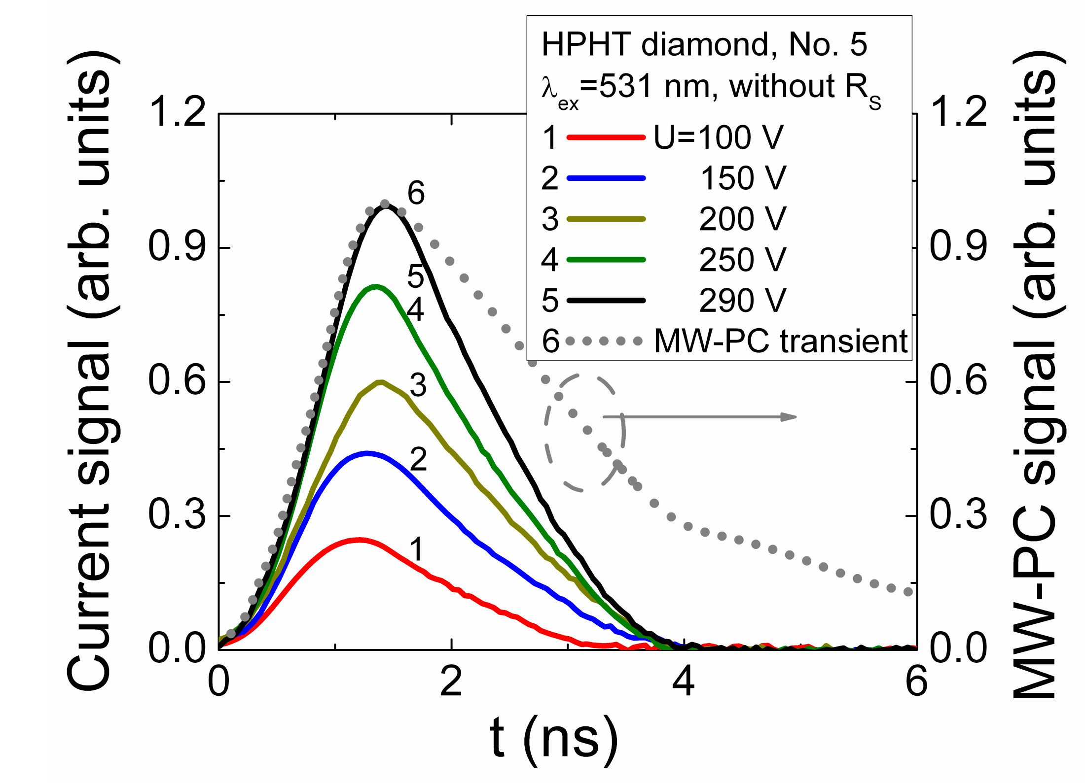
Variation of current transients obtained by changing the fixed values of applied voltage in capacitor type detector made of HPHT diamond sample No. 5 (
Figure 1) is illustrated in
Figure 10. Here, excitation by 531 nm light pulses was implemented. In this case, excess carrier generation from deep centres prevails and a bulk charge domain is injected. The shape of the induced current transients is inherent for the carrier recombination-drift dominated process (discussed in
Section 3.2).
Figure 10.
Variation of the induction current transients dependent on the applied voltage in a capacitor type detector made of a mosaic set of linear implanted contacts and metal electrodes containing HPHT diamond sample No. 5. Injection of excess carriers has been implemented by 531 nm light laser pulses impinging through hole in the electrode.
The initial current peak can be ascribed to the bipolar drift of the injected carriers, where pulse duration and further current decrease can be ascribed to carrier trapping/recombination. The excess carrier density relaxation transient, recorded without external electric field and measured by microwave probed photoconductivity (MW-PC) technique, is additionally shown in
Figure 10 by dot curve. Here, the normalized amplitude of MW-PC signal is exploited to adequately scale the MW-PC and ICDC transients. The range (>100 V) of applied voltages (
Figure 10) was sufficient to get a short (<2 ns) transit time for the drift-recombination of the injected carriers, where the role of the polarization effect is also reduced. The rather large applied voltage determines the sufficiently wide depletion regions (
Xe0,
Xh0) nearby the electrodes. Therefore the current component ascribed to extraction of the diffusion brought carriers is also rather short, and it overlaps with current component attributed to carrier drift. In order to separate different components of the induced current in time scale, where temporal resolution and duration of processes is of the same order of magnitude, the deconvolution of transients has been performed using the parameters of the external circuit and of excitation pulse.
However, it was not possible to clearly discriminate the components of a current transient due to short characteristic times (τ
tr, τ
R) which values are close to the temporal resolution of experimental system. This issue can also be implied from
Figure 10, where no clear shift of the kink point relative to time axis, attributed to arrival of drifting carriers, is resolved when applied voltages have been varied significantly. Such a result hints the competition between the drift and recombination, assumed within equation (Equation (16)). The similar voltage dependent characteristics (transient shapes and temporal parameters) have been obtained for all the investigated HPHT diamond detectors under injection of bulk domains by UV light (354 nm) pulses. These results show that usage of the pressed plate electrodes (pinned to either bare polished wafer samples surfaces—No. 7 and No. 9,
Figure 1—or to additionally metallized surfaces (sample No. 5,
Figure 1)) exhibit the capacitor type detector features.
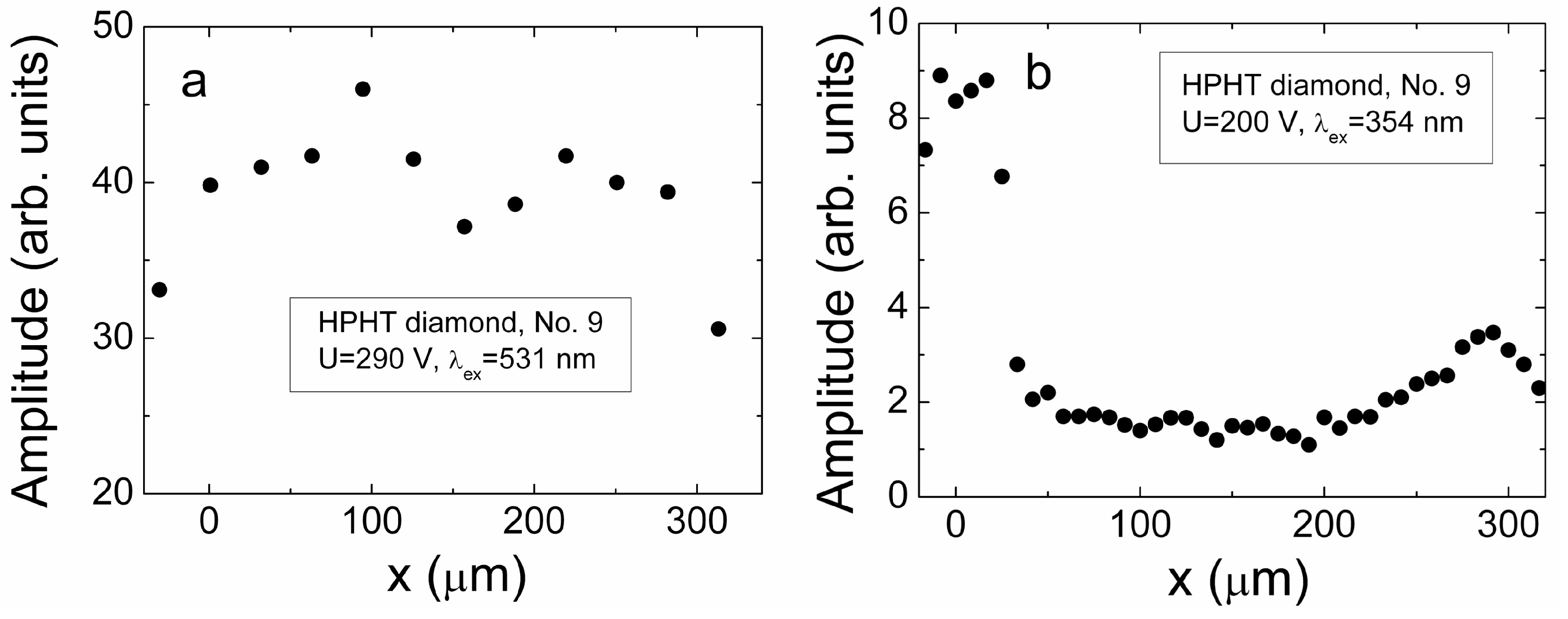
The cross-sectional profiles of the peak values of current induced by scanning location of a focused injection beam of either 531 nm or 354 nm light, obtained for HPHT diamond sample No. 9, are illustrated in
Figure 11a,b, respectively. This sample is rather homogeneous and contains a single growth sector of cubic orientation. A strip focusing regime implemented by a cylindrical lens enables to exclude the impact of the transverse carrier diffusion
Figure 11.
The cross-sectional profiles of the peak values of current induced by scanning location of a focused injection beam of 531 nm (a) and 354 nm (b) light, obtained for HPHT diamond sample No. 9.
Figure 11.
The cross-sectional profiles of the peak values of current induced by scanning location of a focused injection beam of 531 nm (a) and 354 nm (b) light, obtained for HPHT diamond sample No. 9.
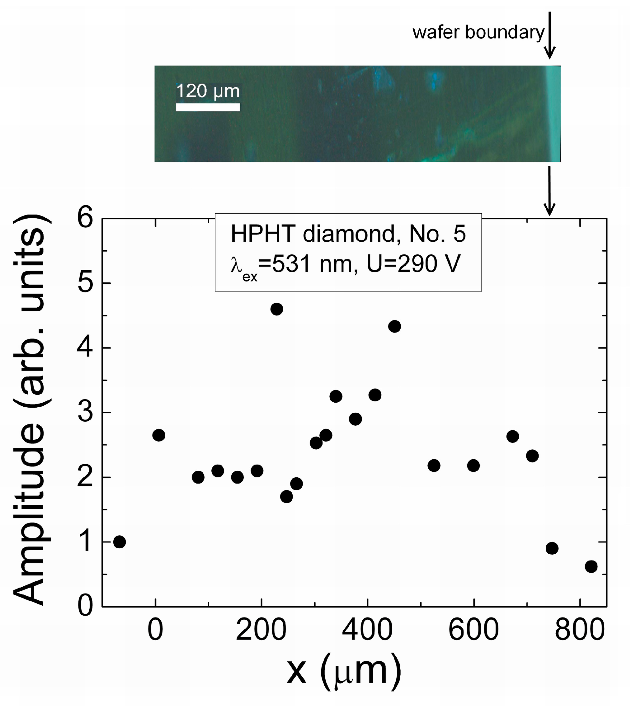
Figure 12.
The cross-sectional profile of the peak values of current induced by scanning location of a focused injection beam of 531 nm light, obtained for HPHT diamond sample No. 5. The microscopy image of wafer boundary taken in UV light for the scanned area is shown on top of the current distribution profile plot, where the extended defects are imaged by luminescence spots (bright-blue) within bulk of wafer.
The profile scanned by using 531 nm (
Figure 11a) light pulses contains a rather flat vertex. This indicates the recombination prevailed drift process. Only shallow sag within the profile vertex can be noticed which can be attributed to a current reduction due to the increased transit time. The profile unveiled by the two-photon bulk domain injection, when using 354 nm (
Figure 11b) light pulses, has a clear relief. The peak values of the induced current are increased by approaching of injection beam location to electrodes. This indicates the prevailing of carrier drift. Then, the current increase at electrodes is explained by the shortest drift path and, thereby, the shortest transit time. Complementarily, these current values are the smallest ones for the injection beam locations in the mid of an inter-electrode gap. Carrier recombination also might be an additional reason for reduction of the collected charge when the drift time is close or even exceeds that of carrier recombination lifetime. The impact of carrier lifetime is the most prominent within cross-sectional profiles scanned on the depth-inhomogeneous HPHT diamond samples. Such an illustration is presented in
Figure 12. This illustration (
Figure 12) shows a cross-sectional profile of the induction current obtained for detector formed on the sample No. 5, where clear inclusion of metallic precipitates were visualized (by microscopy imaging—on top) within sample depth.
The cross-sectional profile (
Figure 12) scanned for this HPHT diamond sample No. 5 shows a random distribution of the current peak values. There is neither enhancement of current due to reduction of transit time when injection location approaches to electrodes nor flat vertex ascribed to homogeneous distribution of defects, acting as the recombination centres. Such a profile qualitatively correlates with cross-sectional wafer image where defects of different size and origin can be resolved.
4.3. Profiling of Current Transients in CVD Diamond
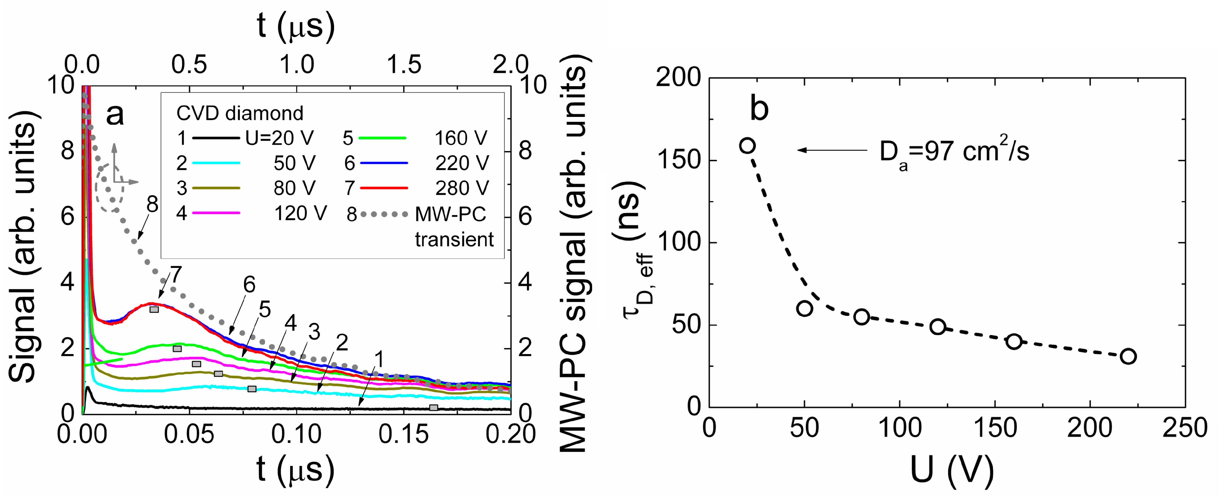
The same (as for HPHT diamond) profiling regimes were applied for capacitor type detector made of CVD diamond. Owing to the considerably longer carrier recombination lifetimes (τ
R ≥ 110 ns,
Figure 13a) in CVD material, the main current components can be resolved by varying profiling regimes. Evolution of the induced current transients, recorded in CVD diamond device profiled at fixed excitation intensity by varying applied voltage, are illustrated in
Figure 13a. The transients displayed within a sub-microsecond time scale enable observation of both current components, namely,
i1 and
i2, discussed in
Section 3.1 (Equation (15)). The peak values of the drift current component
i1 significantly exceed those attributed to the diffusion supplied carrier extraction component
i2. Increasing of the applied voltage leads to an enhancement of a width of the depleted regions at electrodes and of the acting electric field, thereby reducing the time necessary to extract the diffusion supplied carriers. This determines a shift of the peak position ascribed to the
i2 current component towards a time scale of the transit times with enhancement of applied voltage. Thereby, the parameter of an effective time τ
D,eff ascribed diffusion can be introduced. This parameter is determined as a time shift between the current components
i1 and
i2 fixed by their peak values (
i1,peak and
i2,peak). Variation of the drift-diffusion ascribed effective time τ
D,eff as a function of applied voltage is illustrated in
Figure 13b. It can be deduced from
Figure 13b that this τ
D,eff time is weakly dependent on applied voltage for the range of elevated
U > 50 V values, where the excess carrier drift prevails. Contrary, reduction of applied voltage below the
U < 50 V leads to a sharp increase of τ
D,eff up to 150 ns. Unfortunately, this time scale is in the range of the carrier recombination lifetimes in CVD diamond. Therefore, the
i2 signal considerably falls down, and precision of separation of the
i2,peak is improper to proceed measurements at significantly lowered voltages. Nevertheless, τ
D ≌
deff2/4π
2Da values, extracted for the voltage range
U < 50 V, indicate a clear prevalence of diffusion process. This enables estimation of values of a coefficient
Da of the carrier ambipolar diffusion in CVD diamond, assuming that current
i2,peak peak value is attributed to the main (regular regime [
45]) mode (
k = 0) of diffusion in sample with infinite surface recombination. The estimated value of
Da = 97 cm
2/s is in good agreement with those values calculated using the parameters of carrier drift mobilities, published in literature (e.g., [
13]).
Figure 13.
(a) Variation of the current transients recorded in the CVD diamond device by changing bias voltage when excess carrier bulk domain is injected through electrode using UV 354 nm light pulses. Dot-curve, ascribed to the top-right scales, represents relaxation of excess carrier density measured by microwave probed photo-conductivity (MW-PC) technique. It should be noted that the time scale (bottom) for the carrier drift-diffusion transients is considerably shorter than that (top) for MW-PC transient; (b) Diffusion ascribed effective time τD,eff (which is determined as a time shift between the current components (peak values i1,peak and i2,peak) within a long scale of transient display) as a function of applied voltage.
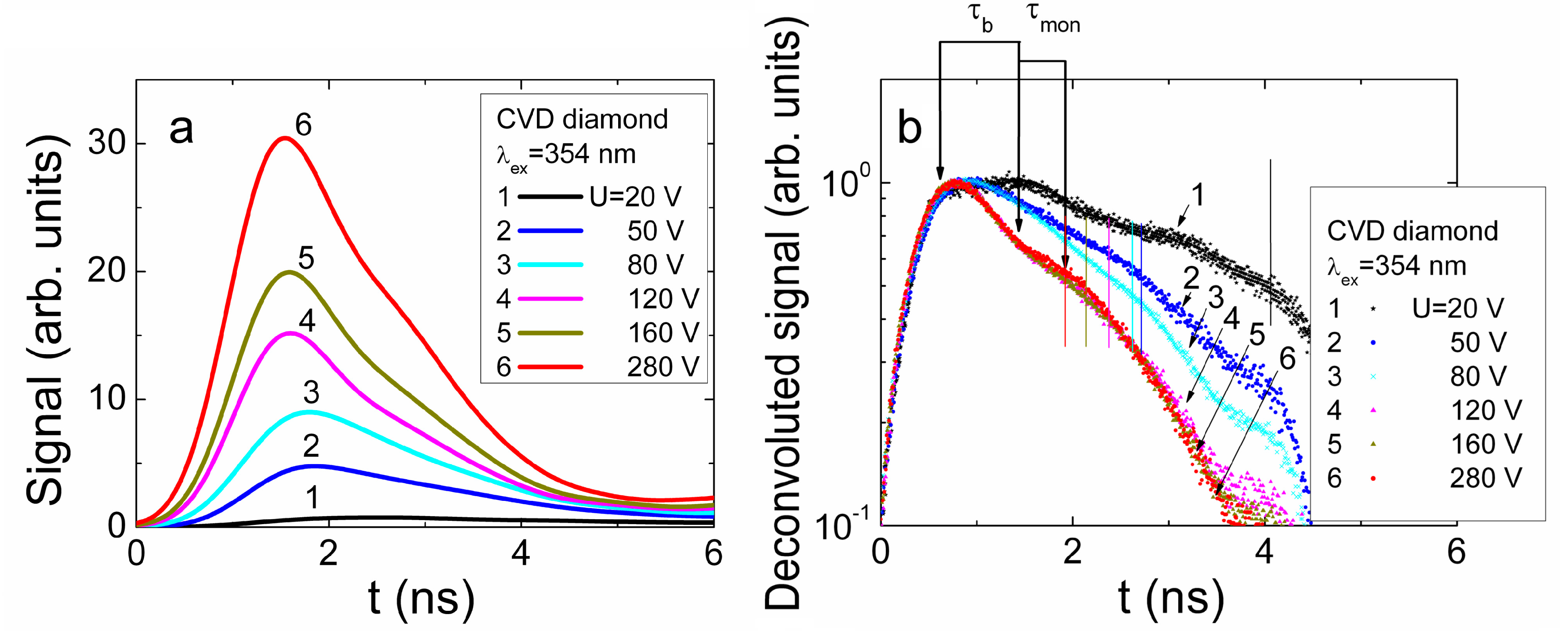
In order to examine the fast current component
i1, current transients were recorded within short (a few ns) display scale, to enhance precision. Evolution of this transient component as a function of applied voltage is represented in
Figure 14a. The asymmetric shape transients (different from those recorded for HPHT diamond), relative to a peak position, were obtained. Unfortunately, due to improper temporal resolution of the experimental arrangement exploited, direct analysis of drift characteristics is impossible. Therefore, the transients have been deconvoluted using Gaussian convolution function with parameters adjusted to the initial delay component correlated with the experimental transients. The deconvoluted transients are illustrated in
Figure 14b. There the initial rise to peak becomes more abrupt. The rearward kink, ascribed to the arrival time of carriers to electrode, can be discriminated. This kink instant on vertex of a current pulse is employed to estimate the transit time which is measured between the initial peak (
i1,peak, this indicates the end of excitation pulse), and the rearward instant of kink formation on vertex of current pulse (which indicates the end of drift). The instant (shown by vertical lines in
Figure 14b) of a kink point depends on applied voltage, and it shifts towards the beginning of current pulse with enhancement of voltage. There the components of the bipolar and monopolar drift can tentatively be implied. However, the unambiguous attribution of these components to the paths of the hole and electron drift and to their transit times is very complicated in the parallel geometry (
Figure 2a) measurement regime. Such changes again have a clear tendency only in the range of elevated voltages
U > 50 V. For the range of
U < 50 V, the amplitude of the deconvoluted transient (curve 1
Figure 14b) increases considerably together with its duration, and this implies an overlap of drift and diffusion governed components in the induced current transients which becomes improper for analysis of transit times.
Figure 14.
(a) Variation of the current transients recorded in short display scale by changing bias voltage when excess carrier bulk domain is injected through electrode using UV 354 nm light pulses; (b) The deconvoluted transients as a function of applied voltage. The bipolar (τb) and monopolar (τmon) drift components are denoted by arrows for drift of electrons within the final phase of transient at U = 280 V.
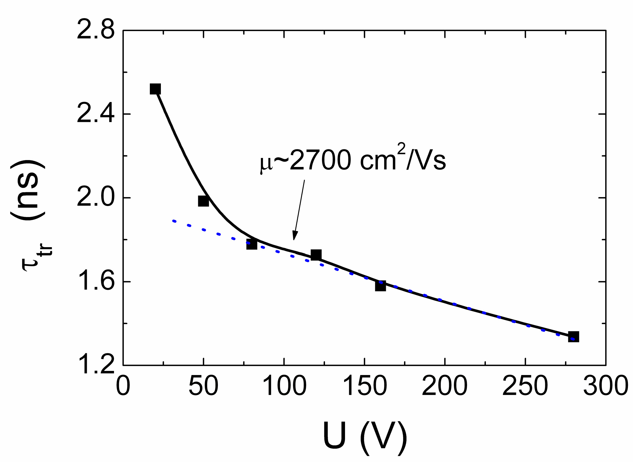
The measured effective transit time as a function of applied voltage is illustrated in
Figure 15. The transit time τ
tr increases almost linearly with reduction of applied voltage (
Figure 15) for the range of voltages U = 75–300 V. There precision of evaluation of the τ
tr falls down in the range of
U > 200 V. There both the extraction depth and an amount of extracted charge become dependent on applied voltage and partially compensate variations of each other, as discussed in
Section 3.1 and
Section 4.1. Nevertheless, the roughly estimated value of carrier mobility μ
≈ [2
X02/(
Uτ
tr)]
≈ 2700 cm
2/Vs within correlated drift of excess carriers is in agreement with mobility values reported in literature (e.g., [
13]). This evolution (
Figure 15) of a short current component enables only estimation of the averaged carrier mobility at assumption of the flat vertex of current pulse from the measured transit time as a function of applied voltage. The assumption of the flat vertex of a current pulse is closely related to the steady-state models where charge supplied from voltage source during carrier drift (to simultaneously keep the invariable applied voltage and the charge conservation under varied CUD capacitance [
38,
39,
40,
48], due to additional light injected charge) is ignored. The widely exploited steady-state models are based on assumption of the independent (non-correlated) drift of holes as well as of electrons and on ignoring of the Shockley-Ramo’s effect—the induction of charge on electrodes due to moving externally injected carriers within inter-electrode space. There TCAD simulations can be exploited (for instance, [
48]) for modelling of the carrier drift process in a steady-state approach. However, the simulated transients using the steady-state and the dynamic models [
48] can considerably differ. In the steady-state approach, the histogram type drift current components for holes and electrons and of their sum appear, as usual.
Figure 15.
The transit time evaluated from the deconvoluted current transients as a function of applied voltage using an approximation of the flat vertex of pulse.
Figure 15.
The transit time evaluated from the deconvoluted current transients as a function of applied voltage using an approximation of the flat vertex of pulse.
The assumption of non-correlated drift of holes and electrons, used in steady-state models, is equivalent to the increased drift path
d∑, as
d∑ = de + dh > d, which exceeds the inter-electrode gap
d. It can alternatively be misinterpreted that the double elementary charge
e,
i.e.,
e × 2, is carried during the bipolar drift of an electron-hole (e-h) pair. However, it can easily be verified (e.g., [
48]) that an e-h pair carries (over the path of the bipolar drift) the same elementary charge
e as either a single hole or electron, which proceeds the charge transport process after one counter-partner of a pair reaches the electrode. Thus, ignoring of the changes of the acting electric field, caused by charge supplied to electrodes from an external voltage source (if carrier injection from electrodes can be ignored for the junction and capacitor type devices), leads to the underestimated carrier mobility values, if
d∑ > d is considered.
In current transients recorded by the cross-sectional profiling of the charge injection location, the injection position and paths of electron and hole drift can definitely be correlated with electrode voltage polarity. In these current transients, recorded by cross-sectional profiling on CVD diamond sample, only a short current component has been observed ascribed to the drift of the separated electron-hole sub-domains. The deconvoluted transients are illustrated in
Figure 16a. The components of the bipolar and monopolar transit times are there also denoted in
Figure 16a. The simulated transients (as that illustrated in
Figure 16a for a single transient) have been employed for evaluation of carrier mobilities using dynamic models mentioned in
Section 3.2 and published in more detail in [
38,
39,
40,
48]. There parameters of the injected charge amount, of the external circuit, of carrier trapping/detrapping and other (ascribed to measurement geometry, voltage,
etc.) have been incorporated. The fitting of the simulated transient to the experimental one at different applied voltages leaded to values of electron (μ
e) and hole (μ
h) mobility values of μ
e = 4000 cm
2/Vs and μ
h = 3800 cm
2/Vs, respectively. The close values of μ
e and of μ
h, nevertheless, lead to a rather flat vertex of the recorded transients. On the other hand, the non-ideality of the experimental conditions and temporal resolution of our experimental circuits complicated a perfect fit of the experimental and simulated transients. For instance, the initial and rear slopes within the deconvoluted transients indicate a non-abrupt strip boundary shape of the focused excitation beams. The separated values of μ
e = 4000 cm
2/Vs and μ
h = 3800 cm
2/Vs by using the cross-sectional profiling of the charge injection location exceed that value μ = 2700 cm
2/Vs extracted from the voltage profiling on CVD diamond sample in parallel measurement geometry. The reason of these deviations, mentioned above, can be explained by non-adequate evaluation of drift paths when parallel measurement geometry is exploited.
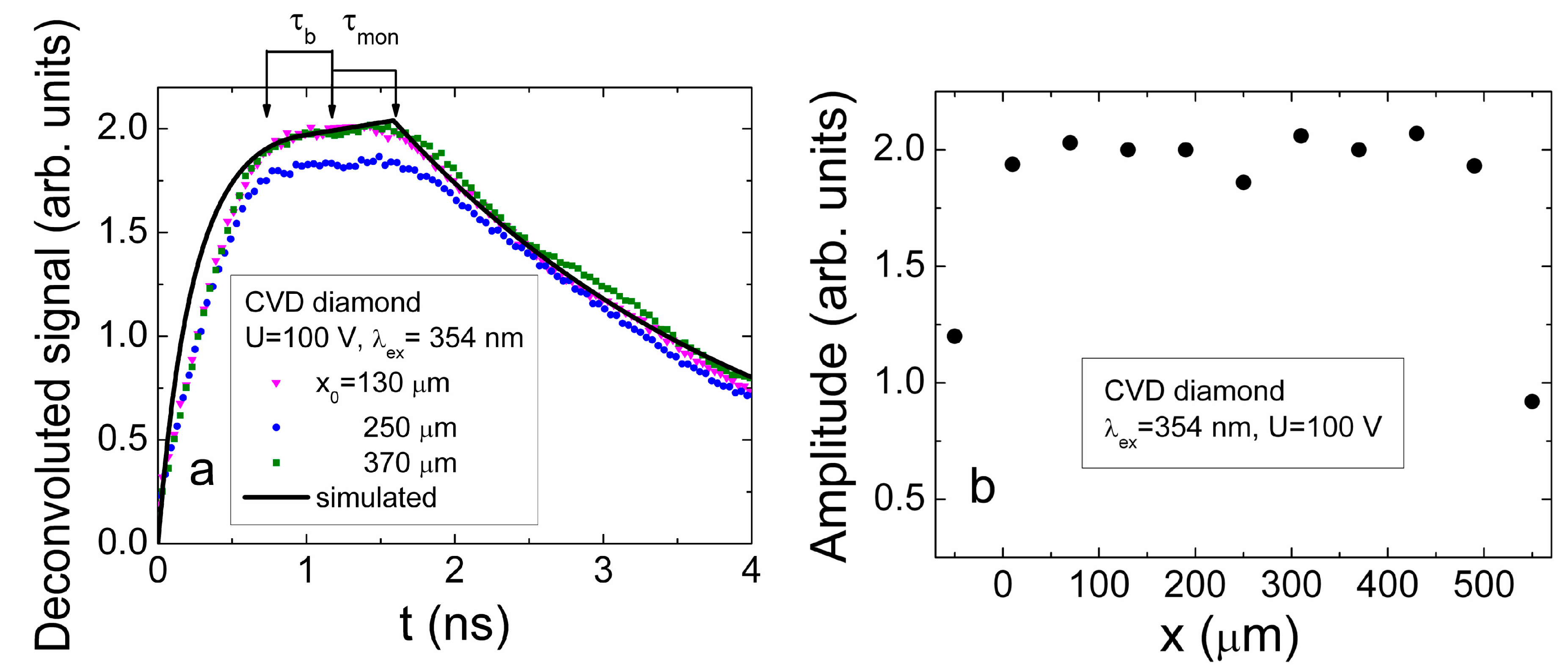
Figure 16.
(a) The deconvoluted current transients for several injection positions recorded within cross-sectional scans of the CVD diamond capacitor type detector. The bipolar (τb) and monopolar (τmon) drift components are denoted by arrows for drift of electrons within the final phase of transient. The solid curve represents a simulated transient for injection location x = 130 μm relatively to the negative electrode at voltage Ubias DC = 100 V; (b) The amplitude of the induced current (ascribed to the bipolar drift component) as a function of the injection position within inter-electrode gap, measured in capacitor type detector made of CVD diamond.
The profile of the induced current amplitude as a function of this beam location also exhibits a rather flat vertex (
Figure 16b). This profile can be understood at assumption of close values of μ
e and of μ
h. Nevertheless, a shallow sag within the profile vertex can there be noticed in
Figure 16b which can be attributed to current reduction due to the increased transit time when excitation beam is localized in the mid of the inter-electrode gap.

