
A Label-Free Impedimetric DNA Sensor Based on a Nanoporous SnO2 Film: Fabrication and Detection Performance


Abstract
:
1. Introduction
2. Experimental Section
2.1. Nanoporous SnO2 Film Deposition
2.2. Functionalization Process
2.2.1. Liquid Phase Deposition
2.2.2. Vapour Phase Deposition

| Complementary | 3' AC CTA TTT GGG TGA GAT AC-Cy3 5' |
|---|---|
| Non-complementary | 3' AC TGG CGC AAT CAC TCT AC-Cy3 5' |
| 1-base mismatch | 3' AC CTA TTT GCG TGA GAT AC-Cy3 5' |
| 2-base mismatch | 3' AC CTA TTT GCA TGA GAT AC-Cy3 5' |
2.3. Characterization Techniques
3. Results and Discussion
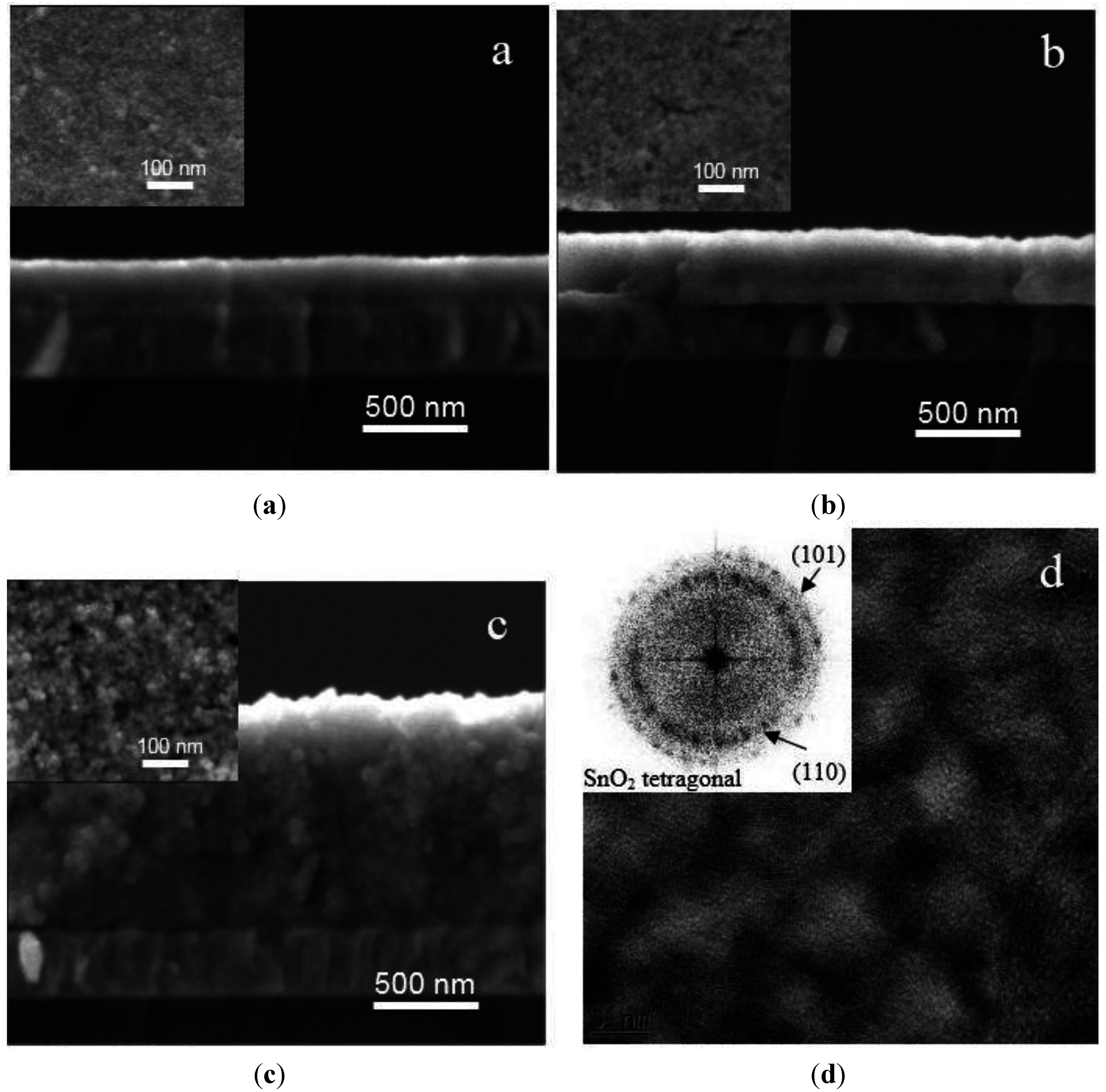
3.1. Bare Electrodeposited SnO2 Film Characteristics
3.2. DNA Hybridization Detection
3.2.1. Influence of Film Thickness on the DNA Hybridization Detection Signals
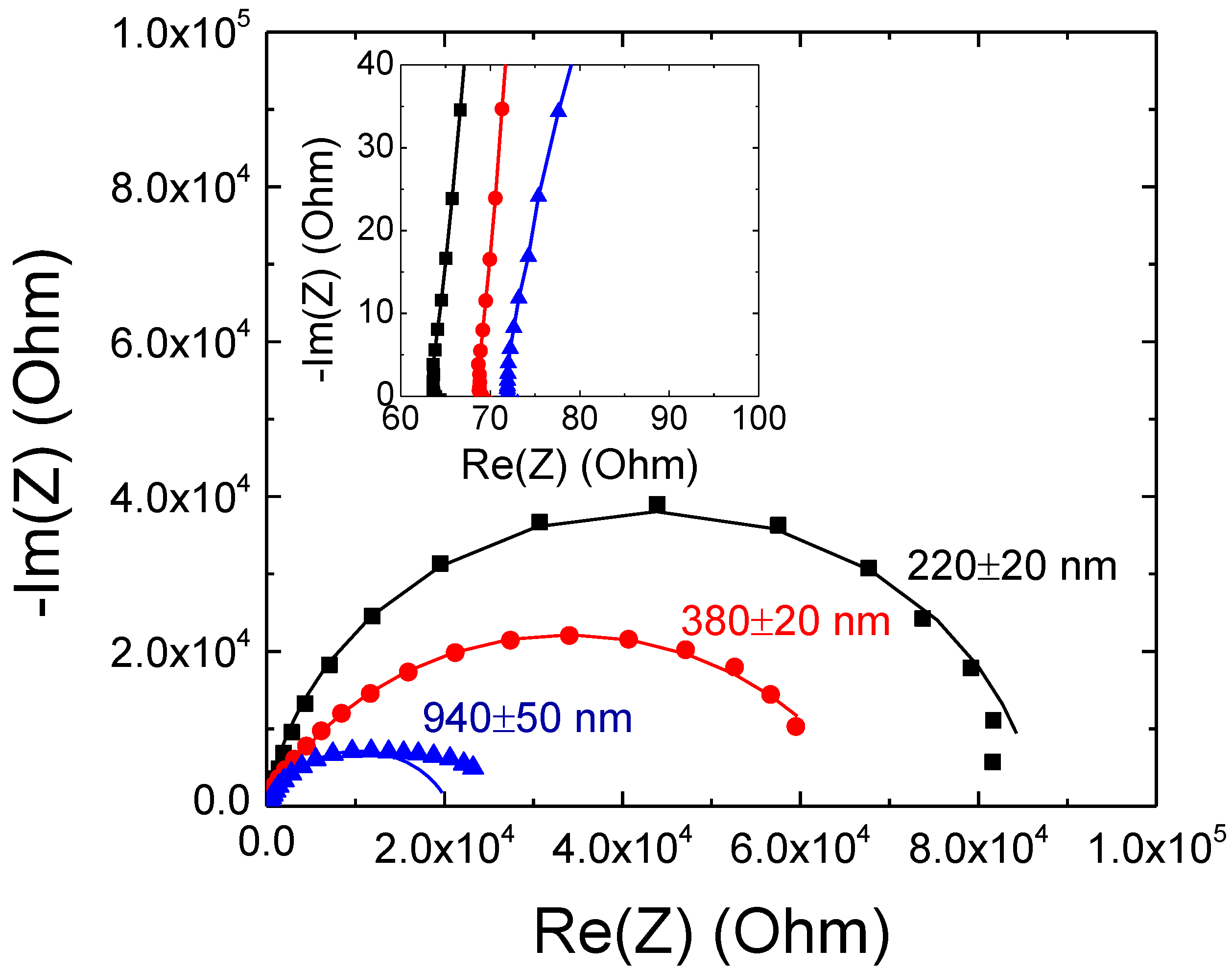
| Q (C/cm2) | Film Thickness (nm) | Re (Ω) | C1 (μF) | α1 | R1 (Ω) |
|---|---|---|---|---|---|
| 0.2 | 220±20 | 64.61 | 23.37 | 0.779 | 84,782 |
| 0.4 | 380±20 | 70.40 | 26.29 | 0.772 | 66,496 |
| 0.8 | 920±50 | 73.90 | 38.15 | 0.810 | 21,276 |

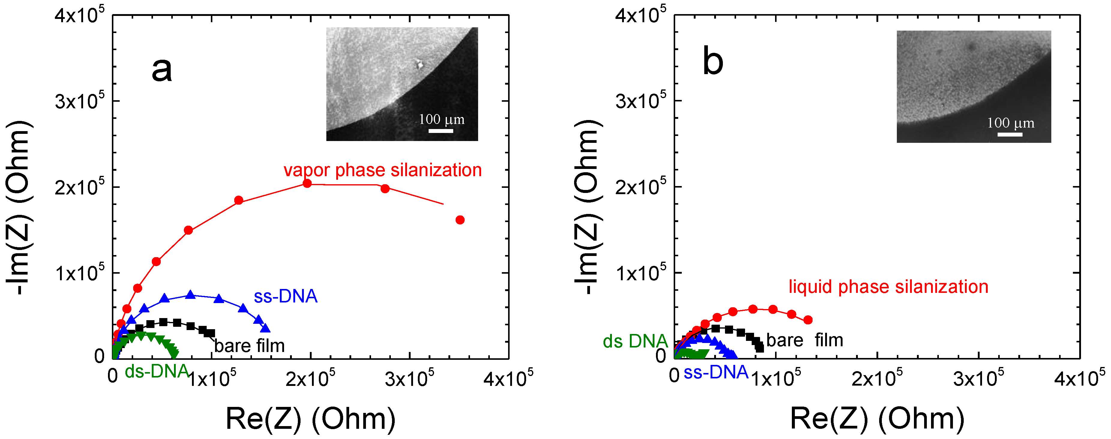
| Film Thickness (nm) | DNA Target Molecules | R1 (Ω) | ∆R1/R1 (%) | |||
|---|---|---|---|---|---|---|
| SnO2 Film | Silanized | ss_DNA | ds_DNA | |||
| 220 ± 20 | complementary | 84782 | 146577 | 51974 | 24743 | −54 ± 5 |
| non-complementary | 87250 | 136078 | 45541 | 42543 | −6 ± 2 | |
| 380 ± 20 | complementary | 66496 | 115162 | 95137 | 43301 | −59 ± 5 |
| non-complementary | 67596 | 127038 | 101959 | 95300 | −5 ± 2 | |
| 940 ± 50 | complementary | 21276 | 47176 | 23047 | 15413 | −33 ± 4 |
| non-complementary | 20486 | 56258 | 28471 | 26605 | −6 ± 2 | |
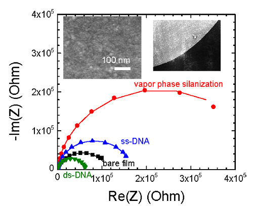
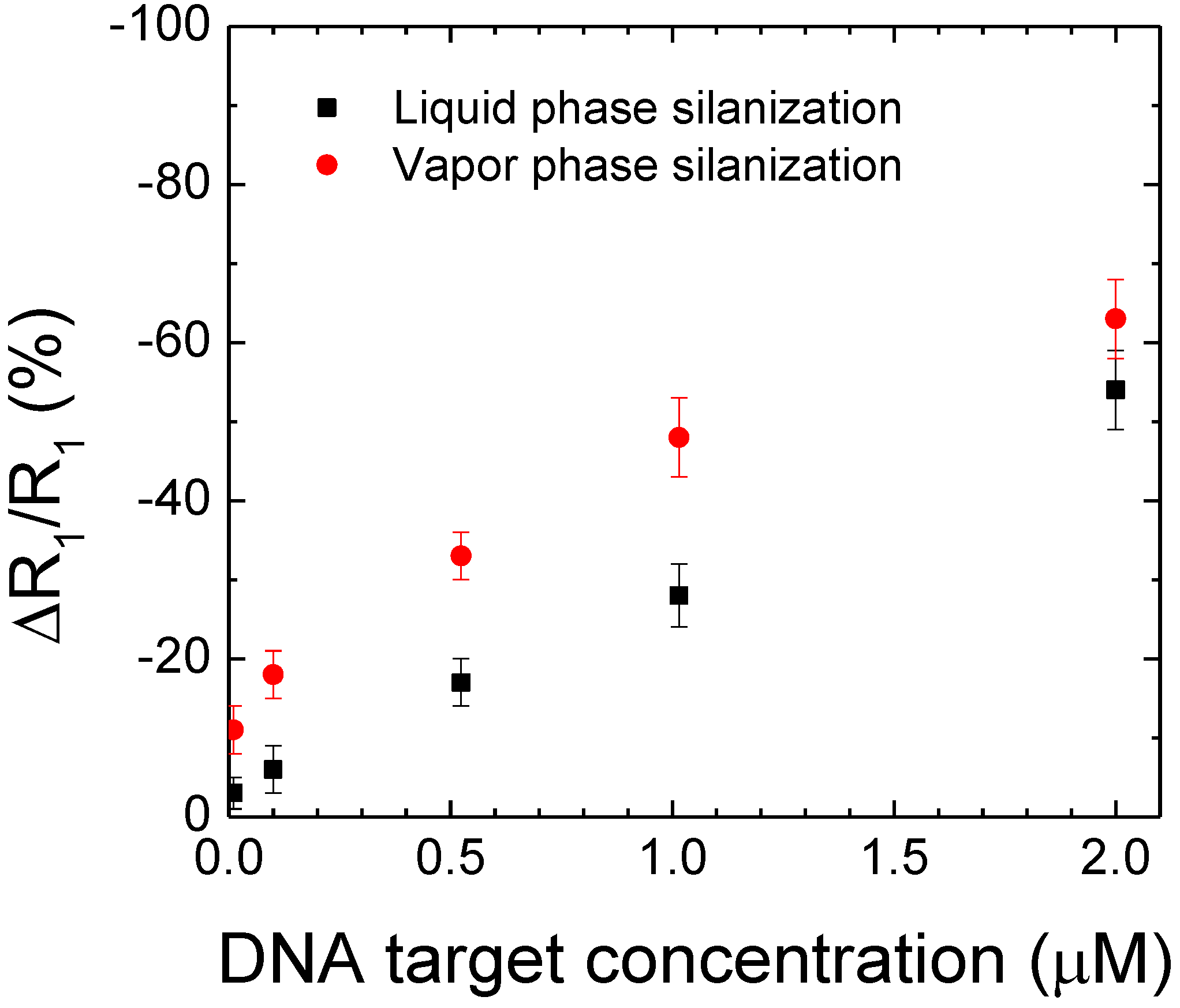
3.2.2. APTES Vapour Phase Deposition vs. Liquid Phase Deposition
| Vapour Phase Silanization | |||||
| CDNA target (μM) | R1 (Ω) | ∆R1/R1 (%) | |||
| SnO2 Film | Silanized | ss_DNA | ds_DNA | ||
| 2.0 | 96,782 | 43,2768 | 167,202 | 61,836 | −63 ± 5 |
| 1.0 | 86,453 | 370,742 | 147,929 | 76,689 | −48 ± 5 |
| 0.5 | 85,310 | 377,590 | 143,687 | 97,006 | −33 ± 3 |
| 0.1 | 81,101 | 416,567 | 121,467 | 99,531 | −18 ± 3 |
| 0.01 | 79,987 | 393,879 | 126,847 | 111,929 | −11 ± 3 |
| Liquid Phase Silanization | |||||
| CDNA target (μM) | R1 (Ω) | ∆R1/R1 (%) | |||
| SnO2 Film | Silanized | ss_DNA | ds_DNA | ||
| 1.0 | 97,419 | 144,626 | 47,492 | 34,015 | −28 ± 5 |
| 0.5 | 97,926 | 151,935 | 45,305 | 37,707 | −17 ± 3 |
| 0.1 | 95,509 | 135,238 | 43,923 | 40,441 | −7 ± 2 |
| 0.01 | 95,264 | 141,849 | 48,337 | 47,538 | −2 ± 1 |

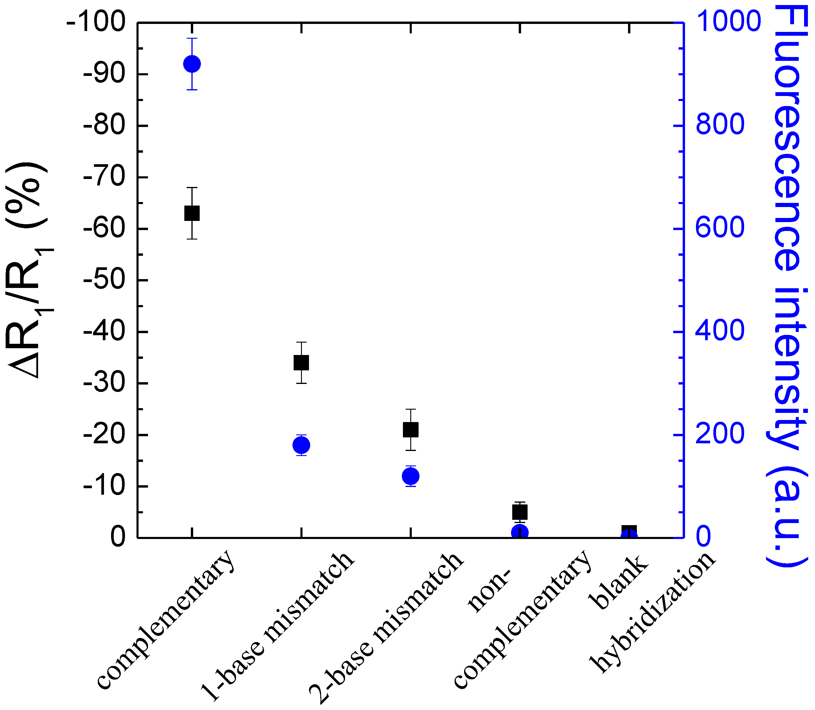
| DNA Target Molecule | CDNA target (μM) | R1 (Ω) | ∆R1/R1 (%) | |||
|---|---|---|---|---|---|---|
| SnO2 Film | Silanized | ssDNA | dsDNA | |||
| 1-base mismatch | 2.0 | 98742 | 356254 | 120292 | 79007 | −34 ± 5 |
| 2-base mismatch | 97249 | 374519 | 109624 | 86879 | −21 ± 4 | |
| Blank hybridization (buffer without DNA target) | 87876 | 381906 | 105884 | 99632 | −1 ± 0.5 | |
4. Conclusions
Acknowledgments
Author Contributions
Conflicts of Interest
References
- Sassolas, A.; Leca-Bouvier, B.D.; Blum, L.J. DNA Biosensors and Microarrays. Chem. Rev. 2008, 108, 109–139. [Google Scholar] [CrossRef] [PubMed]
- Livache, T.; Bazin, H.; Mathis, G. Conducting polymers on microelectronic devices as tools for biological analyses. Clin. Chim. Acta 1998, 278, 171–176. [Google Scholar] [CrossRef] [PubMed]
- Kushon, S.A.; Ley, K.D.; Bradford, K.; Jones, R.M.; McBranch, D.; Whitten, D. Detection of DNA hybridization via fluorescent polymer superquenching. Langmuir 2002, 18, 7245–7249. [Google Scholar] [CrossRef]
- Azek, F.; Grossiord, C.; Joannes, M.; Limoges, B.; Brossier, P. Hybridization Assay at a Disposable Electrochemical Biosensor for the Attomole Detection of Amplified Human Cytomegalovirus DNA. Anal. Biochem. 2000, 284, 107–113. [Google Scholar] [CrossRef] [PubMed]
- Fortin, E.; Mailley, P.; Lacroix, L.; Szunerits, S. Imaging of DNA hybridization on microscopic polypyrrole patterns using scanning electrochemical microscopy (SECM): The HRP bio-catalyzed oxidation of 4-chloro-1-naphthol. Analyst 2006, 131, 186–193. [Google Scholar] [CrossRef] [PubMed]
- Ferreira, H.A.; Cardoso, F.A.; Ferreira, R.; Cardoso, S.; Freitas, P.P. Magnetoresistive DNA chips based on ac field focusing of magnetic labels. J. Appl. Phys. 2006, 99. [Google Scholar] [CrossRef]
- Cai, H.; Wang, Y.; He, P.; Fang, Y. Electrochemical detection of DNA hybridization based on silver-enhanced gold nanoparticle label. Anal. Chim. Acta 2002, 469, 165–172. [Google Scholar] [CrossRef]
- Peng, H.; Soeller, C.; Cannell, M.B.; Bowmaker, G.A.; Cooney, R.P.; Travas-Sejdic, J. Electrochemical detection of DNA hybridization amplified by nanoparticles. Biosens. Bioelectron. 2006, 21, 1727–1736. [Google Scholar] [CrossRef] [PubMed]
- Stambouli, V.; Labeau, M.; Matko, I.; Chenevier, B.; Renault, O.; Guiducci, C.; Chaudouët, P.; Roussel, H.; Nibkin, D.; Dupuis, E. Development and functionalisation of Sb doped SnO2 thin films for DNA biochip applications. Sens. Actuators B Chem. 2006, 113, 1025–1033. [Google Scholar] [CrossRef]
- Daniels, J.S.; Pourmand, N. Label-Free Impedance Biosensors: Opportunities and Challenges. Electroanalysis 2007, 19, 1239–1257. [Google Scholar] [CrossRef] [PubMed]
- Ansari, A.A.; Singh, R.; Sumana, G.; Malhotra, B.D. Sol–gel derived nano-structured zinc oxide film for sexually transmitted disease sensor. Analyst 2009, 134, 997. [Google Scholar] [CrossRef] [PubMed]
- Patel, M.K.; Singh, J.; Singh, M.K.; Agrawal, V.V.; Ansari, S.G.; Malhotra, B.D. Tin Oxide Quantum Dot Based DNA Sensor for Pathogen Detection. J. Nanosci. Nanotechnol. 2013, 13, 1671–1678. [Google Scholar] [CrossRef] [PubMed]
- Popovich, N.D.; Eckhardt, A.E.; Mikulecky, J.C.; Napier, M.E.; Thomas, R.S. Electrochemical sensor for detection of unmodified nucleic acids. Talanta 2002, 56, 821–828. [Google Scholar] [CrossRef] [PubMed]
- Yang, I.V.; Thorp, H.H. Modification of Indium Tin Oxide Electrodes with Repeat Polynucleotides: Electrochemical Detection of Trinucleotide Repeat Expansion. Anal. Chem. 2001, 73, 5316–5322. [Google Scholar] [CrossRef] [PubMed]
- Park, J.Y.; Park, S.M. DNA hybridization sensors based on electrochemical impedance spectroscopy as a detection tool. Sensors 2009, 9, 9513–9532. [Google Scholar] [CrossRef] [PubMed]
- Lazerges, M.; Bedioui, F. Analysis of the evolution of the detection limits of electrochemical DNA biosensors. Anal. Bioanal. Chem. 2013, 405, 3705–3714. [Google Scholar] [CrossRef] [PubMed]
- Christine Berggren, P.S. A Feasibility Study of a Capacitive Biosensor for Direct Detection of DNA Hybridization. Electroanalysis 1999, 11, 156–160. [Google Scholar] [CrossRef]
- Lai, W.A.; Lin, C.H.; Yang, Y.S.; Lu, M.S.C. Ultrasensitive and label-free detection of pathogenic avian influenza DNA by using CMOS impedimetric sensors. Biosens. Bioelectron. 2012, 35, 456–460. [Google Scholar] [CrossRef] [PubMed]
- Tlili, C.; Korri-Youssoufi, H.; Ponsonnet, L.; Martelet, C.; Jaffrezic-Renault, N.J. Electrochemical impedance probing of DNA hybridisation on oligonucleotide-functionalised polypyrrole. Talanta 2005, 68, 131–137. [Google Scholar] [CrossRef] [PubMed]
- Gautier, C.; Cougnon, C.; Pilard, J.F.; Casse, N. Label-free detection of DNA hybridization based on EIS investigation of conducting properties of functionalized polythiophene matrix. J. Electroanal. Chem. 2006, 587, 276–283. [Google Scholar] [CrossRef]
- Gautier, C.; Esnault, C.; Cougnon, C.; Pilard, J.F.; Casse, N.; Chénais, B. Hybridization-induced interfacial changes detected by non-Faradaic impedimetric measurements compared to Faradaic approach. J. Electroanal. Chem. 2007, 610, 227–233. [Google Scholar] [CrossRef] [Green Version]
- Souteyrand, E.; Cloarec, J.P.; Martin, J.R.; Wilson, C.; Lawrence, I.; Mikkelsen, S.; Lawrence, M.F. Direct Detection of the Hybridization of Synthetic Homo-Oligomer DNA Sequences by Field Effect. J. Phys. Chem. B 1997, 101, 2980–2985. [Google Scholar] [CrossRef]
- Cloarec, J.P.; Martin, J.R.; Polychronakos, C.; Lawrence, I.; Lawrence, M.F.; Souteyrand, E. Functionalization of Si/SiO2 substrates with homooligonucleotides for a DNA biosensor. Sens. Actuators B Chem. 1999, 58, 394–398. [Google Scholar] [CrossRef]
- Chen, C.P.; Ganguly, A.; Lu, C.Y.; Chen, T.Y.; Kuo, C.C.; Chen, R.S.; Tu, W.H.; Fischer, W.B.; Chen, K.H.; Chen, L.C. Ultrasensitive in situ Label-Free DNA Detection Using a GaN Nanowire-Based Extended-Gate Field-Effect-Transistor Sensor. Anal. Chem. 2011, 83, 1938–1943. [Google Scholar] [CrossRef] [PubMed]
- Cai, W.; Peck, J.R.; van der Weide, D.W.; Hamers, R.J. Direct electrical detection of hybridization at DNA-modified silicon surfaces. Biosens. Bioelectron. 2004, 19, 1013–1019. [Google Scholar] [CrossRef] [PubMed]
- Vamvakaki, V.; Chaniotakis, N.A. DNA Stabilization and Hybridization Detection on Porous Silicon Surface by EIS and Total Reflection FT-IR Spectroscopy. Electroanalysis 2008, 20, 1845–1850. [Google Scholar] [CrossRef]
- Yang, W.; Butler, J.E.; Russell, John N.; Hamers, R.J. Interfacial Electrical Properties of DNA-Modified Diamond Thin Films: Intrinsic Response and Hybridization-Induced Field Effects. Langmuir 2004, 20, 6778–6787. [Google Scholar] [CrossRef] [PubMed]
- Vermeeren, V.; Bijnens, N.; Wenmackers, S.; Daenen, M.; Haenen, K.; Williams, O.A.; Ameloot, M.; vandeVen, M.; Wagner, P.; Michiels, L. Towards a Real-Time, Label-Free, Diamond-Based DNA Sensor. Langmuir 2007, 23, 13193–13202. [Google Scholar] [CrossRef] [PubMed]
- Chen, C.P.; Ganguly, A.; Wang, C.H.; Hsu, C.W.; Chattopadhyay, S.; Hsu, Y.K.; Chang, Y.C.; Chen, K.H.; Chen, L.C. Label-Free Dual Sensing of DNA Molecules Using GaN Nanowires. Anal. Chem. 2009, 81, 36–42. [Google Scholar] [CrossRef] [PubMed]
- Zebda, A.; Stambouli, V.; Labeau, M.; Guiducci, C.; Diard, J.P.; le Gorrec, B. Metallic oxide CdIn2O4 films for the label free electrochemical detection of DNA hybridization. Biosens. Bioelectron. 2006, 22, 178–184. [Google Scholar] [CrossRef] [PubMed]
- Zebda, A.; Labeau, M.; Diard, J.P.; Lavalley, V.; Stambouli, V. Electrical resistivity dependence of semi-conductive oxide electrode on the label-free electrochemical detection of DNA. Sens. Actuators B Chem. 2010, 144, 176–182. [Google Scholar] [CrossRef]
- Stambouli, V.; Zebda, A.; Appert, E.; Guiducci, C.; Labeau, M.; Diard, J.-P.; Le Gorrec, B.; Brack, N.; Pigram, P.J. Semiconductor oxide based electrodes for the label-free electrical detection of DNA hybridization: Comparison between Sb doped SnO2 and CdIn2O4. Electrochimica Acta 2006, 51, 5206–5214. [Google Scholar] [CrossRef]
- Abdelkader, Z. Propriétés Microstructurales et Electriques D’Electrodes D’Oxydes SnO2 et Cdln2O4: Application à la Détection Electrochimique Directe de L’Hybridation de l’ADN. Ph.D. Thesis, INPG, Grenoble, France, 2007. [Google Scholar]
- Le, M.H.; Fradetal, L.; Delabouglise, D.; Mai, A.T.; Stambouli, V. Fluorescence and label free impedimetric DNA detection on SnO2 nanopillars. Electroanalysis 2015, in press. [Google Scholar]
- Therese, G.H.A.; Kamath, P.V. Electrochemical Synthesis of Metal Oxides and Hydroxides. Chem. Mater. 2000, 12, 1195–1204. [Google Scholar] [CrossRef]
- Chang, S.T.; Leu, I.C.; Hon, M.H. Preparation and Characterization of Nanostructured Tin Oxide Films by Electrochemical Deposition. Electrochem. Solid -State Lett. 2002, 5, C71–C74. [Google Scholar] [CrossRef]
- Piro, B.; Haccoun, J.; Pham, M.C.; Tran, L.D.; Rubin, A.; Perrot, H.; Gabrielli, C. Study of the DNA hybridization transduction behavior of a quinone-containing electroactive polymer by cyclic voltammetry and electrochemical impedance spectroscopy. J. Electroanal. Chem. 2005, 577, 155–165. [Google Scholar] [CrossRef]
- Anne, A.; Bouchardon, A.; Moiroux, J. 3’-ferrocene-labeled oligonucleotide chains end-tethered to gold electrode surfaces: Novel model systems for exploring flexibility of short DNA using cyclic voltammetry. J. Am. Chem. Soc. 2003, 125, 1112–1113. [Google Scholar] [CrossRef] [PubMed]
- Fiorilli, S.; Rivolo, P.; Descrovi, E.; Ricciardi, C.; Pasquardini, L.; Lunelli, L.; Vanzetti, L.; Pederzolli, C.; Onida, B.; Garrone, E. Vapor-phase self-assembled monolayers of aminosilane on plasma-activated silicon substrates. J. Colloid Interface Sci. 2008, 321, 235–241. [Google Scholar] [CrossRef] [PubMed]
© 2015 by the authors; licensee MDPI, Basel, Switzerland. This article is an open access article distributed under the terms and conditions of the Creative Commons Attribution license (http://creativecommons.org/licenses/by/4.0/).
Share and Cite
Le, M.H.; Jimenez, C.; Chainet, E.; Stambouli, V. A Label-Free Impedimetric DNA Sensor Based on a Nanoporous SnO2 Film: Fabrication and Detection Performance. Sensors 2015, 15, 10686-10704. https://doi.org/10.3390/s150510686
Le MH, Jimenez C, Chainet E, Stambouli V. A Label-Free Impedimetric DNA Sensor Based on a Nanoporous SnO2 Film: Fabrication and Detection Performance. Sensors. 2015; 15(5):10686-10704. https://doi.org/10.3390/s150510686
Chicago/Turabian StyleLe, Minh Hai, Carmen Jimenez, Eric Chainet, and Valerie Stambouli. 2015. "A Label-Free Impedimetric DNA Sensor Based on a Nanoporous SnO2 Film: Fabrication and Detection Performance" Sensors 15, no. 5: 10686-10704. https://doi.org/10.3390/s150510686
APA StyleLe, M. H., Jimenez, C., Chainet, E., & Stambouli, V. (2015). A Label-Free Impedimetric DNA Sensor Based on a Nanoporous SnO2 Film: Fabrication and Detection Performance. Sensors, 15(5), 10686-10704. https://doi.org/10.3390/s150510686