
A High Performance LIA-Based Interface for Battery Powered Sensing Devices


Abstract
:1. Introduction
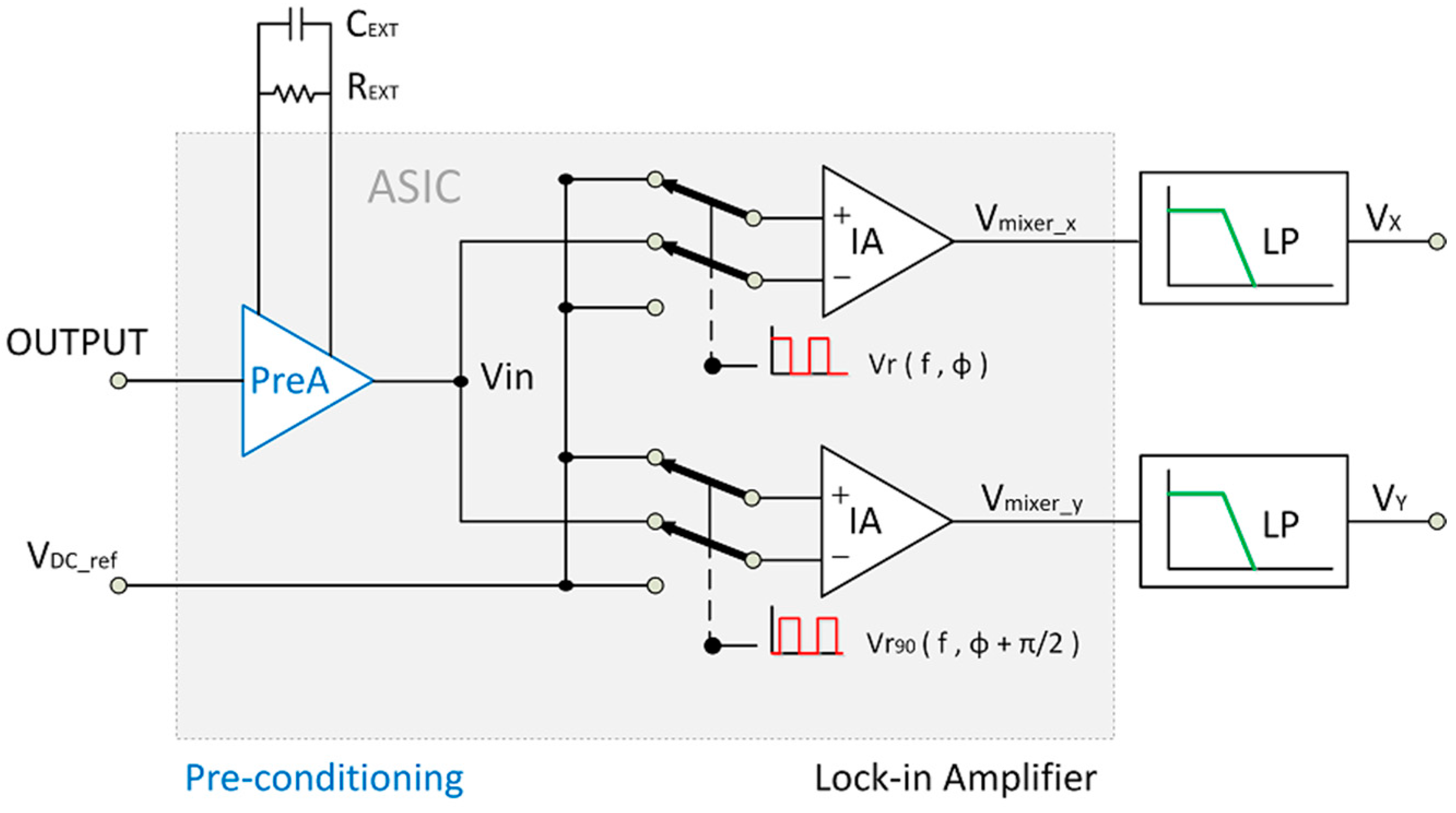
2. Interface Design
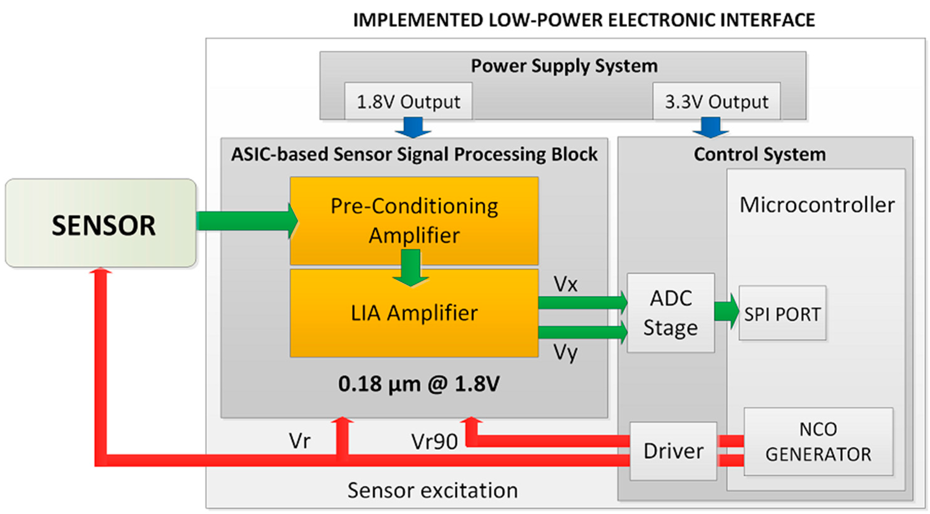
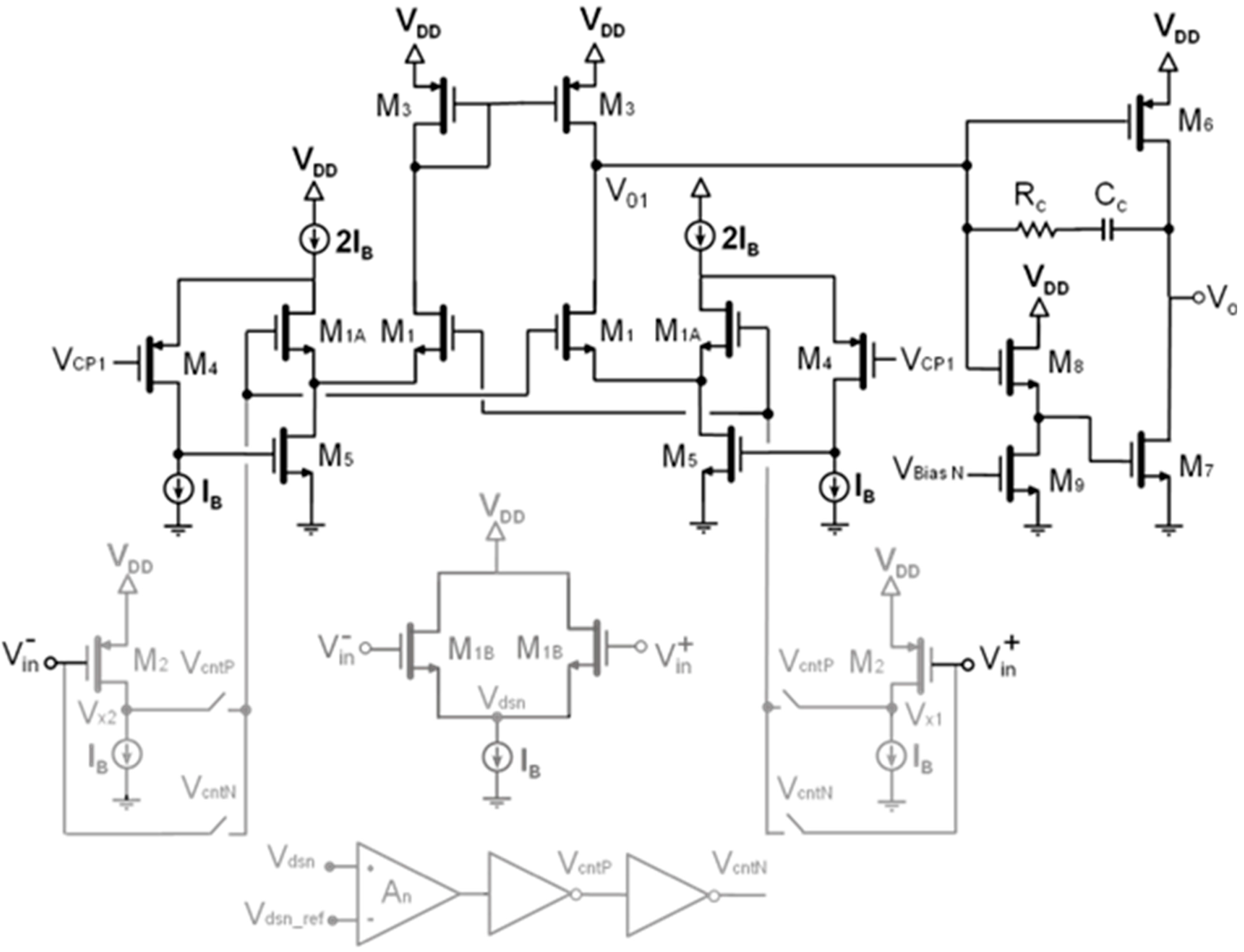
2.1. Sensor Signal Processing System

| VX | VY | A | φ |
|---|---|---|---|

| CMOS Process | 0.18 μm |
| Supply | 1.8 V |
| Open Loop Aain | 74 dB * |
| Gain-Bandwidth Product | 2 MHz |
| CMRR | 96 dB * |
| Slew-Rate | 2.3 V/μs (for a capacitive load of 1 nF) |
| THD | −62 dB (1 kHz, 1.75 Vpp) |
| Input Common-Mode Range | Rail-to-rail |
| Output Swing | Rail-to-rail |
| Input Referred Noise | 63 nV/Hz1/2* (100 kHz) |
| Power | 468 μW |
2.2. Control System
2.3. Power Supply System
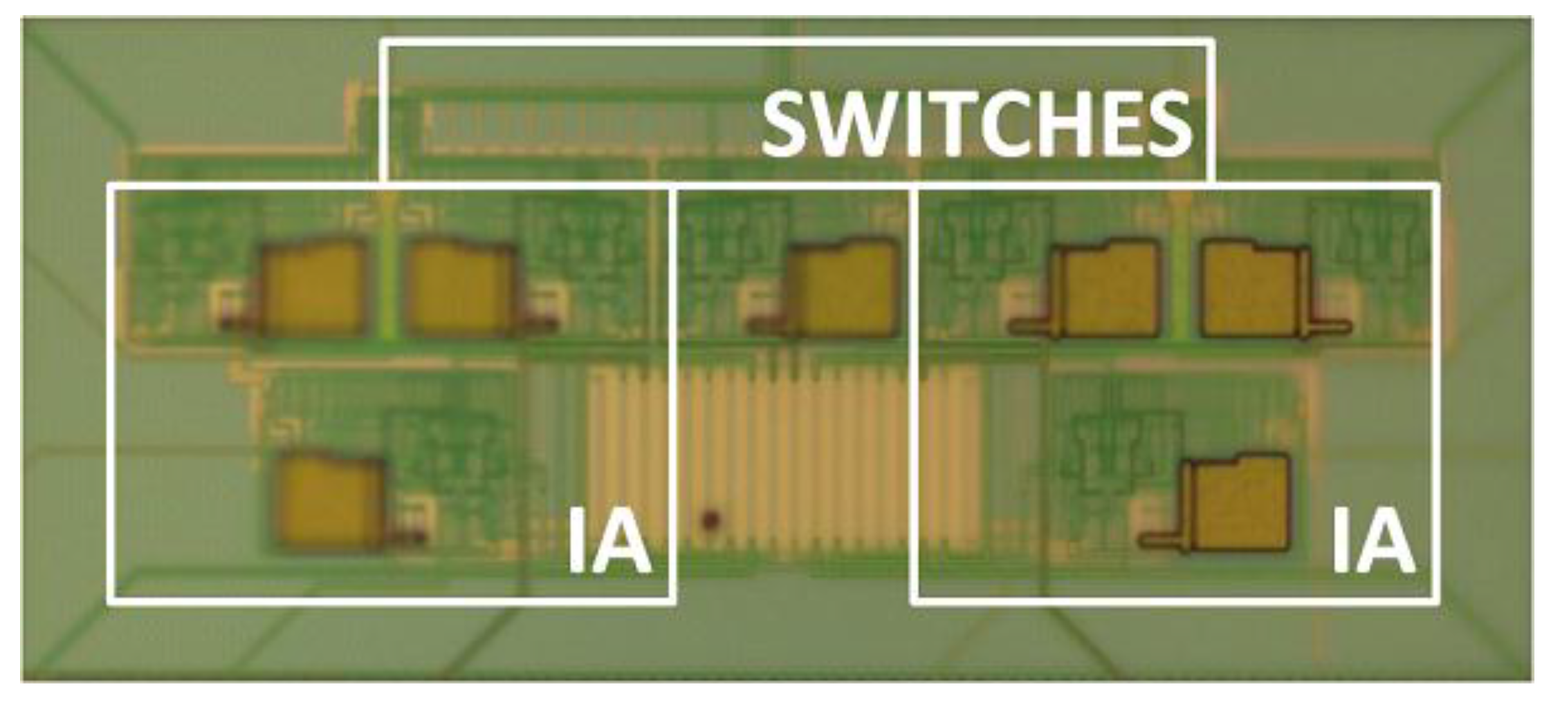
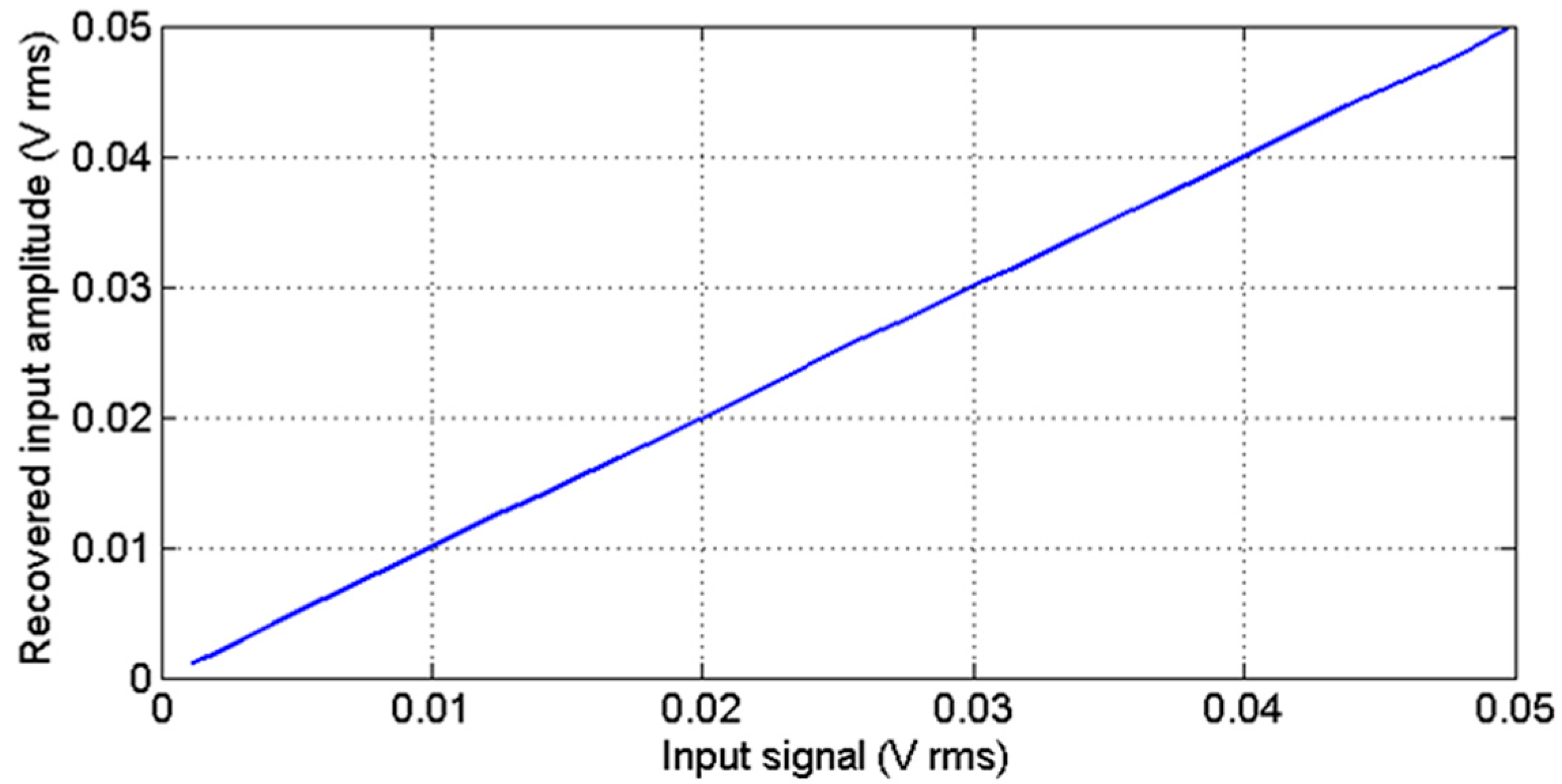
3. Experimental Verification
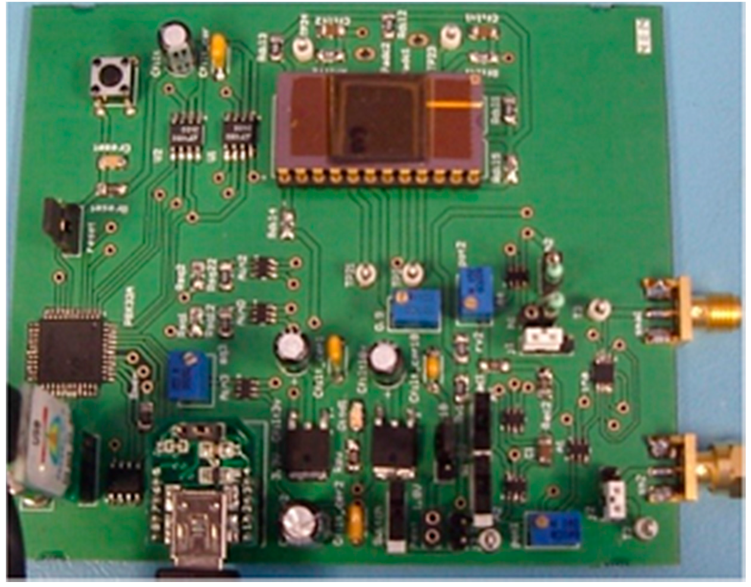

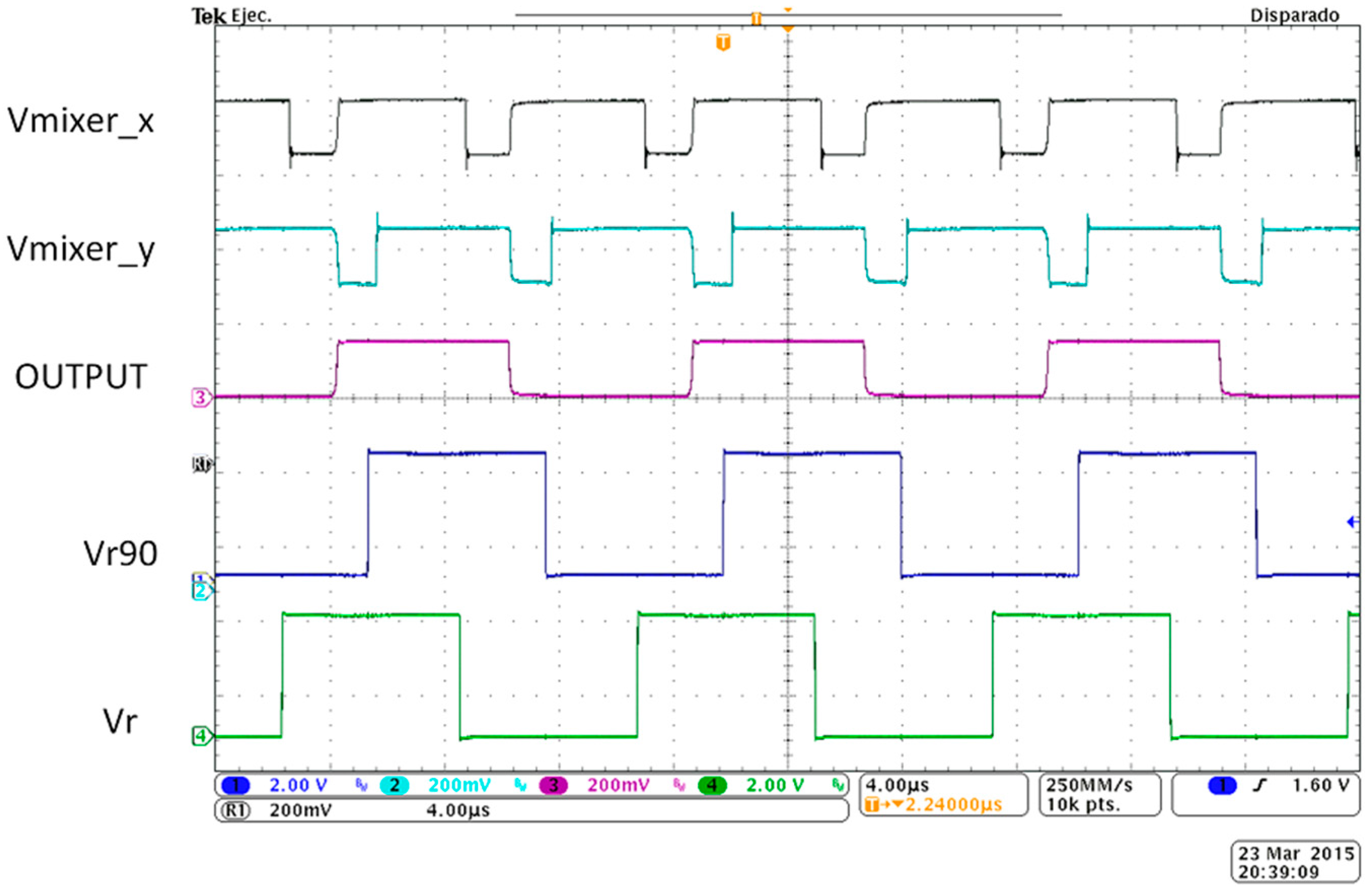
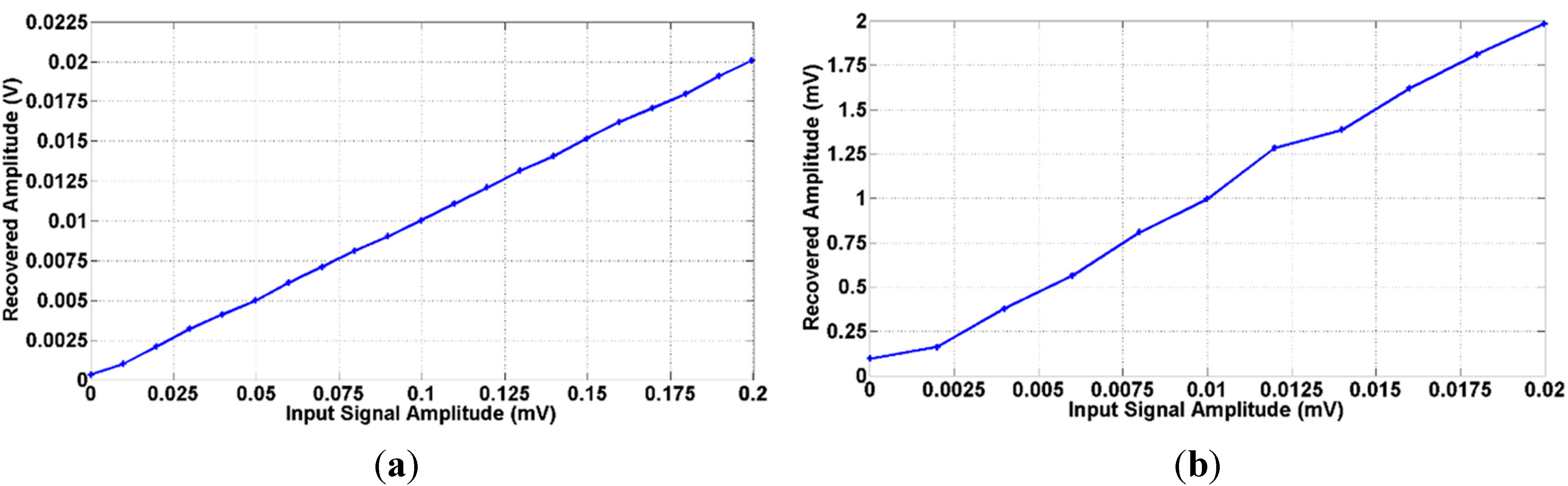
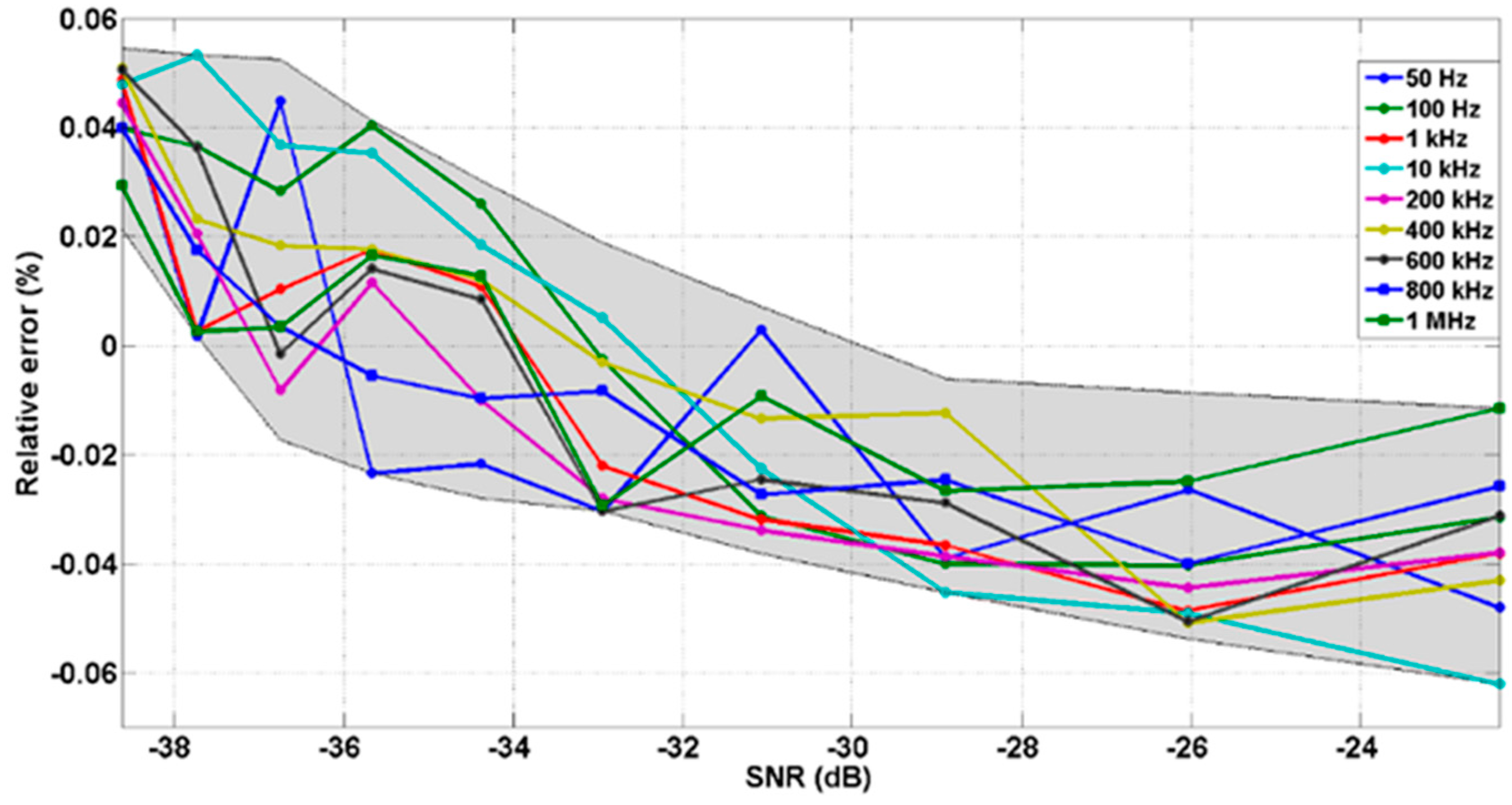
3.1. Interface Performances
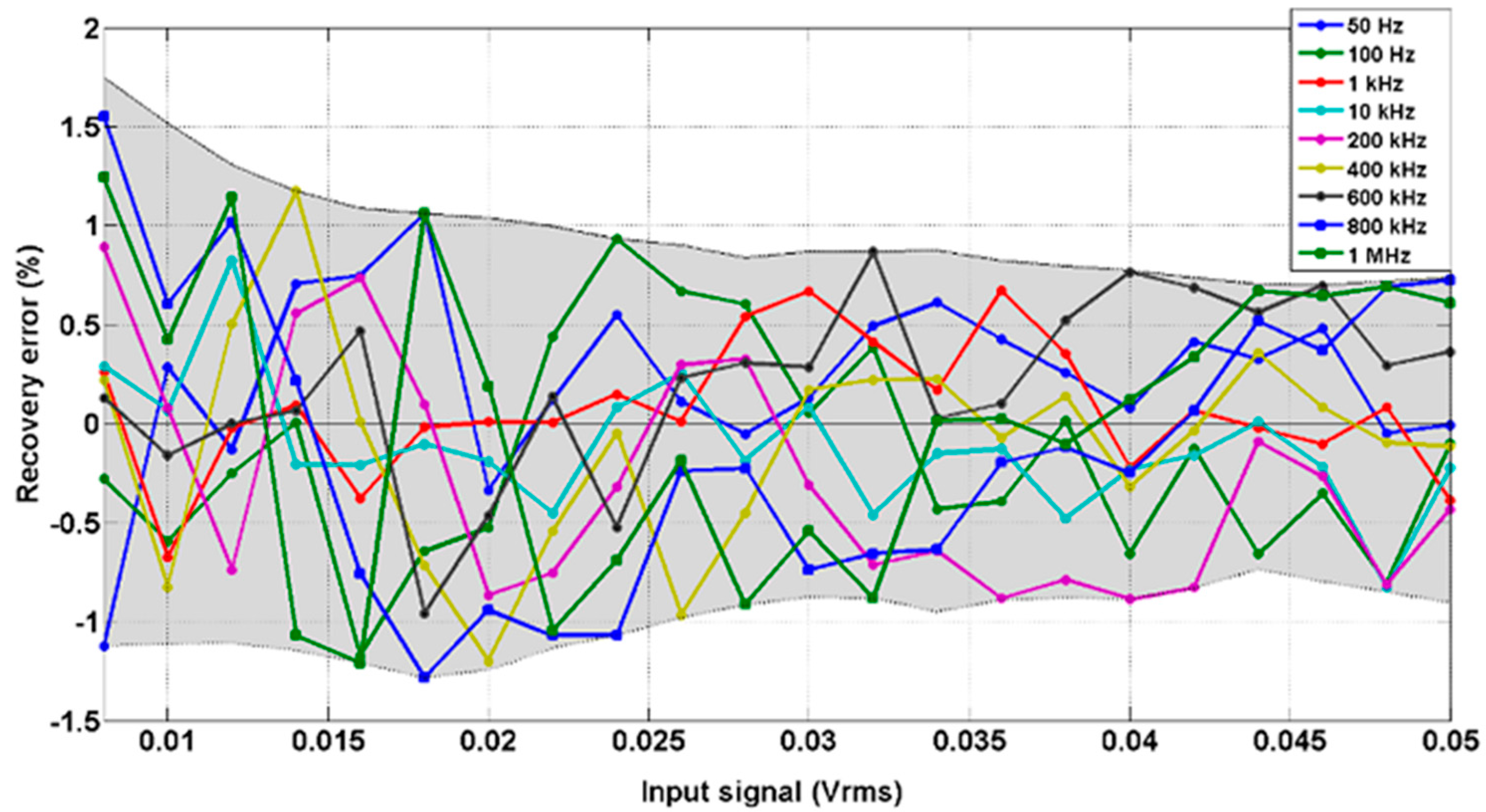

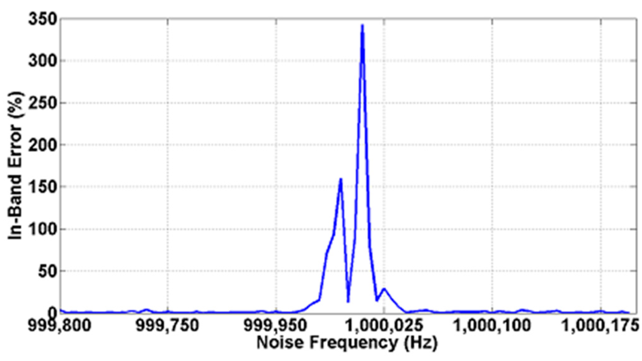
3.2. Noise and Interference Tests


| Operating Frequency | Harmonic | Max. in-Band Error (%) | Dead Band Span (Hz) |
|---|---|---|---|
| 10 kHz | First | >100 | 35 |
| Third | 50 | 40 | |
| Fifth | 30 | 40 | |
| 100 kHz | First | >100 | 40 |
| Third | 58 | 45 | |
| Fifth | 51 | 40 | |
| 1 MHz | First | >100 | 45 |
| Performance | Proposed LIA | [16] (2010) | [17] (2013) | [21] (2014) |
|---|---|---|---|---|
| CMOS Technology (µm) | 0.18 | 0.35 | 0.35 | 0.18 |
| Supply Voltage (V) | 1.8 | ±1 | 1.8 | 1.8 |
| SNR (dB) | −39{ε < 0.07%} | - | - | −42.13 {ε < 4.1%} |
| Resolution (µV) | 1 | 1 | - | 50 |
| Input Signal Type | Sine, Square | Sine | Sine | Sine |
| Frequency Range (kHz) | 1000 | 0.077 | 0.25 | 125 |
| Power Consumption (mW) | <3.5 (2 branches) | 3 (1 branch) | 2 (1 branch) | 0.417 (1 branch) |
| Integrated Area (mm2) | 0.048 | 5 | - | 0.013 |
4. Application to a Microcantilever-Based Resonant Sensor
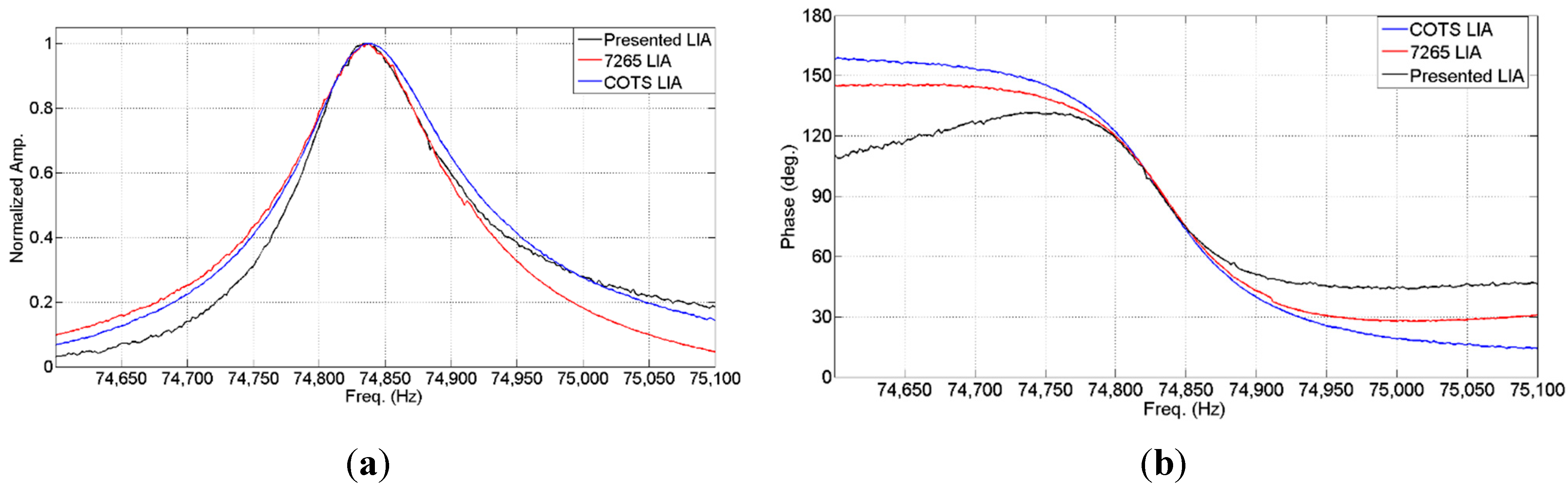
| Integrated-LIA | LIA7265 | COTS Prototype |
|---|---|---|
| f0 = 74,839 Hz | f0 = 74,838 Hz | f0 = 74,840 Hz |
| LIA Implementations | Power (W) | Bandwidth (MHz) |
|---|---|---|
| LIA7265 | 30 | 0.25 |
| COTS Prototype | 0.008 | 0.3 |
| Integrated LIA | 0.0035 | 1.0 |
5. Conclusions
Acknowledgments
Author Contributions
Conflicts of Interest
References
- Lee, E.A.; Seshia, S.A. Introduction to Embedded Systems: A Cyber-Physical Systems Approach; Lee & Seshia: Berkeley, CA, USA, 2011. [Google Scholar]
- Ali, S.; Qaisar, S.B.; Saeed, H.; Farhan Khan, M.; Naeem, M.; Anpalagan, A. Network Challenges for Cyber Physical Systems with Tiny Wireless Devices: A Case Study on Reliable Pipeline Condition Monitoring. Sensors 2015, 15, 7172–7205. [Google Scholar] [CrossRef] [PubMed]
- Stoppe, J.; Drechsler, R. Analyzing SystemC Designs: SystemC Analysis Approaches for Varying Applications. Sensors 2015, 15, 10399–10421. [Google Scholar] [CrossRef] [PubMed]
- Lee, E.A. The Past, Present and Future of Cyber-Physical Systems: A Focus on Models. Sensors 2015, 15, 4837–4869. [Google Scholar] [CrossRef] [PubMed]
- Lee, E.A. Cyber physical systems: Design challenges. In Proceedings of the 11th IEEE International Symposium on Object Oriented Real-Time Distributed Computing (ISORC 2008), Orlando, FL, USA, 5–7 May 2008; pp. 363–369.
- Chen, P.-Y.; Yang, S.; McCann, J.A. Distributed Real-time Anomaly Detection in Networked Industrial Sensing Systems. IEEE Trans. Ind. Electron. 2014, 62, 1. [Google Scholar] [CrossRef]
- About Lock-in amplifiers. Available online: http://www.thinksrs.com/downloads/PDFs/ ApplicationNotes/AboutLIAs.pdf (accessed on 1 August 2014).
- Blair, D.P; Sydenham, P.H. Phase sensitive detection as a means to recover signals buried in noise. J. Phys. E Sci. Instrum. 1975, 8, 621–627. [Google Scholar] [CrossRef]
- Ordonez, M.; Sonnaillon, M.O.; Quaioe, J.E.; Iqbal, M.T. An embedded frequency response analyzer for fuel cell monitoring and characterization. IEEE Trans. Ind. Electron. 2010, 57, 1925–1934. [Google Scholar] [CrossRef]
- Akin, B.; Orguner, U.; Toliyat, H.A.; Rayner, M. Phase-sensitive detection on motor fault signatures in the presence of noise. IEEE Trans. Ind. Electron. 2008, 55, 2539–2550. [Google Scholar] [CrossRef]
- Aguirre, J.; Medrano, N.; Calvo, B.; Celma, S. Lock-in amplifier for portable sensing systems. Electron. Lett. 2011, 47, 1172–1173. [Google Scholar] [CrossRef]
- Valero, M.R.; Celma, S.; Medrano, N.; Calvo, B. A CMOS 1.2-V 1.7-mW lock-in amplifier for sensing applications up to 0.7 MHz. In Proceedings of the 2014 IEEE Sensors, Valencia, Spain, 2–5 November 2014.
- Gnudi, A.; Colalongo, L.; Baccarani, G. Integrated lock-in amplifier for sensor applications. In Proceedings of the IEEE Solid-State Circuits Conference (ESSCIRC), Duisburg, Germany, 21–23 September 1999; pp. 58–61.
- Xu, J.; Meynants, G.; Merken, P. Low-power lock-in amplifier for complex impedance measurement. In Proceedings of the IEEE Workshop on Advances in Sensors and Interfaces (IWASI), Trani, Italy, 25–26 June 2009; pp. 110–114.
- Ferri, G.; de Laurentiis, P.; D’Amico, A.; di Natale, C. A low-voltage integrated CMOS analog lock-in amplifier prototype for LAPS applications. Sens. Actuators A Phys. 2001, 92, 263–272. [Google Scholar] [CrossRef]
- D’Amico, A.; de Marcellis, A.; di Carlo, C.; di Natale, C.; Ferri, G.; Martinelli, E.; Paolesse, R.; Stornelli, V. Low-voltage low-power integrated analog lock-in amplifier for gas sensor applications. Sens. Actuators B Chem. 2010, 144, 400–406. [Google Scholar] [CrossRef]
- De Marcellis, A.; Ferri, G.; Mantenuto, P.; D’Amico, A. A new single-chip analog lock-in amplifier with automatic phase and frequency tuning for physical/chemical noisy phenomena detection. In Proceedings of the IEEE Workshop on Advances in Sensors and Interfaces (IWASI), Bari, Italy, 13–14 June 2013; pp. 121–124.
- Manzaneque, T.; Ruiz-Diez, V.; Hernando-Garcia, J.; Wistrela, E.; Kucera, M.; Schmid, U.; Sanchez-Rojas, J.L. Density-viscosity sensor based on piezoelectric MEMS resonator and oscillator circuit. In Proceedings of the 2014 IEEE Sensors, Valencia, Spain, 2–5 November 2014.
- Urbiztondo, M.A.; Peralta, A.; Pellejero, I.; Sese, J.; Pina, M.P.; Dufour, I.; Santamaria, J. Detection of organic vapours with Si cantilevers coated with inorganic (zeolites) for organic (polymer) layers. Sens. Actuators B Chem. 2012, 171–172, 822–831. [Google Scholar] [CrossRef]
- Valero, M.R.; Celma, S.; Medrano, N.; Calvo, B. OpAmp design for lock-in amplifiers in portable sensing systems. In Proceedings of the 2013 European Conference on Circuit Theory and Design (ECCTD), Dresden, Germany, 8–12 September 2013; pp. 1–4.
- Maya-Hernández, P.M.; Álvarez-Simón, L.C.; Sanz-Pascual, M.T.; Calvo-López, B. An Integrated Low-Power Lock-In Amplifier and Its Application to Gas Detection. Sensors 2014, 14, 15880–15899. [Google Scholar] [CrossRef] [PubMed]
- Aguirre, J.; García-Romeo, D.; Medrano, N.; Calvo, B.; Celma, S. Square-signal-based algorithm for analog lock-in amplifiers. IEEE Trans. Ind. Electron. 2014, 61, 5590–5598. [Google Scholar] [CrossRef]
- García-Romeo, D.; Pellejero, I.; Urbiztondo, M.A.; Sesé, J.; Pina, M.P.; Martínez, P.A.; Calvo, B.; Medrano, N. Portable low-power electronic interface for explosive detection using microcantilevers. Sens. Actuators B Chem. 2014, 200, 31–38. [Google Scholar] [CrossRef]
- Valero, M.R.; Román-Loera, A.; Ramírez-Angulo, J.; López-Martín, A.; Carvajal, R.G. Constant gm rail-to-rail CMOS OpAmp with only one differential pair and switched level shifters. In Proceedings of the 2015 IEEE International Symposium on Circuits and Systems (ISCAS), Lisbon, Portugal, 24–27 May 2015; pp. 2461–2464.
- Sklorz, A.; Janssen, S.; Lang, W. Detection limit improvement for NDIR ethylene gas detectors using passive approaches. Sens. Actuators B Chem. 2012, 175, 246–254. [Google Scholar] [CrossRef]
- Lee, H.J.; Park, K.K.; Oralkan, Ö.; Kupnik, M.; Khuri-Yakub, B.T. A Multichannel Oscillator for a Resonant Chemical Sensor System. IEEE Trans. Ind. Electron. 2014, 61, 5632–5640. [Google Scholar] [CrossRef]
- Langfelder, G.; Caspani, A.; Tocchio, A. Design Criteria of Low-Power Oscillators for Consumer-Grade MEMS Resonant Sensors IEEE Trans. Ind. Electron. 2014, 61, 567–574. [Google Scholar] [CrossRef]
© 2015 by the authors; licensee MDPI, Basel, Switzerland. This article is an open access article distributed under the terms and conditions of the Creative Commons Attribution license (http://creativecommons.org/licenses/by/4.0/).
Share and Cite
García-Romeo, D.; Valero, M.R.; Medrano, N.; Calvo, B.; Celma, S. A High Performance LIA-Based Interface for Battery Powered Sensing Devices. Sensors 2015, 15, 25260-25276. https://doi.org/10.3390/s151025260
García-Romeo D, Valero MR, Medrano N, Calvo B, Celma S. A High Performance LIA-Based Interface for Battery Powered Sensing Devices. Sensors. 2015; 15(10):25260-25276. https://doi.org/10.3390/s151025260
Chicago/Turabian StyleGarcía-Romeo, Daniel, María R. Valero, Nicolás Medrano, Belén Calvo, and Santiago Celma. 2015. "A High Performance LIA-Based Interface for Battery Powered Sensing Devices" Sensors 15, no. 10: 25260-25276. https://doi.org/10.3390/s151025260
APA StyleGarcía-Romeo, D., Valero, M. R., Medrano, N., Calvo, B., & Celma, S. (2015). A High Performance LIA-Based Interface for Battery Powered Sensing Devices. Sensors, 15(10), 25260-25276. https://doi.org/10.3390/s151025260