Performance of SOI Bragg Grating Ring Resonator for Nonlinear Sensing Applications


 and
and 
Abstract
: In this paper, a spectroscopic sensor formed by a silicon-on-insulator waveguiding Bragg grating ring resonator working in linear and non-linear regime is proposed. In linear regime, the device shows a spectral response characterized by a photonic band gap (PBG). Very close to the band gap edges, the resonant structure exhibits split modes having a splitting magnitude equal to the PBG spectral extension, whose characteristics can be exploited to obtain a RI optical sensor almost insensitive to the fabrication tolerances and environmental perturbations. When the device operates in nonlinear regime, exactly in the spectral region showing the split resonant modes, the RI sensing performance is strongly improved with respect to the linear regime. This improvement, demonstrated by taking into account all the non-linear effects excited in the integrated silicon structure (i.e., Two Photon Absorption (TPA), TPA-induced Free Carrier Absorption, plasma dispersion, Self-Phase-Modulation and Cross-Phase-Modulation effects as induced by Kerr nonlinearity) as well as the deleterious thermal and stress effects, allows enhancing the performance of the RI split mode resonant sensors, while achieving good immunity to the fabrication tolerances and environmental perturbations. The improvement in terms of sensor resolution can be at least one order of magnitude, still without using optimal parameters.
1. Introduction
Optical ring resonators are fundamental devices for many Physics and Engineering application fields, ranging from quantum information [1], cavity optomechanics [2], telecommunications [3], to biochemistry [4–7]. Several configurations of optical ring resonators have been investigated and designed, whose modal and resonance spectral features strongly depend on geometrical parameters and physical effects involved. For example, the Fano resonances [4,5] and the Vernier effect [6] have been investigated in order to enhance the sensing performance of photonic sensors based on resonant microcavities. A detection limit enhancement in the nanoparticle (NP) sizing has been experimentally demonstrated by analyzing the split modes [8] arising from the presence of a NP along the perimeter of a Whispering Gallery Mode (WGM) cavity. Moreover, a self-referencing sensing scheme, based on the resonance splitting, has also been exploited to investigate the response of an optofluidic cavity system [9], where a common-mode noise suppression has been achieved by using two coupled ring resonators. Recently, the model and the experimental demonstration of an optical strain sensor formed by including a Fiber Bragg Grating (FBG) in a closed fiber loop has been carried out [10]. The spectral response shows a resonance splitting, associated with the degeneracy removal of two counter-propagating modes, which depend on FBG physical parameters. This splitting variation can therefore be used to sense the strain applied to the resonator in the region where the FBG is written, without suffering from the influence of fiber length variations due to any environmental perturbation. In addition, taking into account the increasing interest widely devoted to Silicon on Insulator (SOI) technology in the last decade [11], the development of photonic sensors based on this platform could induce a boost in the integration of electronic and photonic in one chip for ultra-high performance and very innovative sensing applications [12,13]. By considering together the advantages offered from the optical sensors exploiting split resonance mode structures [7–10] and those offered from SOI technology [11–13], we propose a SOI Bragg Microcavity Resonator (BMR) operating in linear and nonlinear regime to be used in RI sensing applications. Thus, the paper is organized as follows. In Section 2, we explain the physical operation of the device and briefly summarize the mathematical model to investigate the nonlinear effects occurring in the BMR device. The proposed modelling includes all nonlinear effects involved in the integrated silicon structure, i.e., Two Photon Absorption (TPA), Free Carrier Absorption (FCA) induced by TPA, plasma dispersion effect, Self-Phase-Modulation (SPM) and Cross-Phase-Modulation (XPM) effects as induced by Kerr nonlinearity, and the grating coupling effects between clockwise and counter-clockwise waves. In addition, the model takes into account the mismatch between the input beam wavelengths and the microcavity resonance wavelengths, the coupling mechanism between the microcavity and input/output bus waveguide, and the temperature and stress effects on both optical guiding properties and nonlinear effective modal area characterizing the guiding structures. In Section 3, a number of numerical results are shown in order to evidence the physical features and the sensor operation. Moreover, a parametric investigation to find out the sensor design guidelines is carried out as well. Finally, Section 4 summarizes the conclusions.
2. Modeling of SOI Bragg Microcavity Resonator
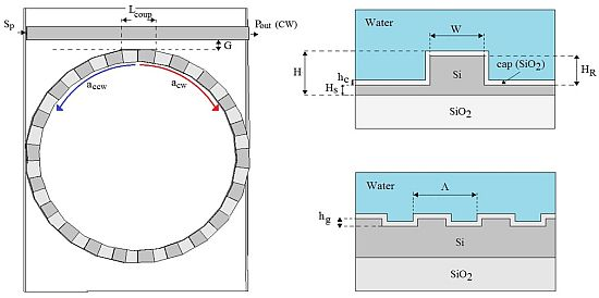
In this section, we briefly explain the nature of the splitting in a Bragg Microcavity Resonator (BMR) and propose the mathematical model to analyse the features occurring in a SOI BMR operating in linear and nonlinear regimes. The BMR geometry in sketched in Figure 1a, where a single bus waveguide is used to couple the input beam (Sp) into the ring resonator having a cavity length (Lcavity) equal to an integer number of the grating period (Λ). The grating depth is hg, as shown in Figure 1c.
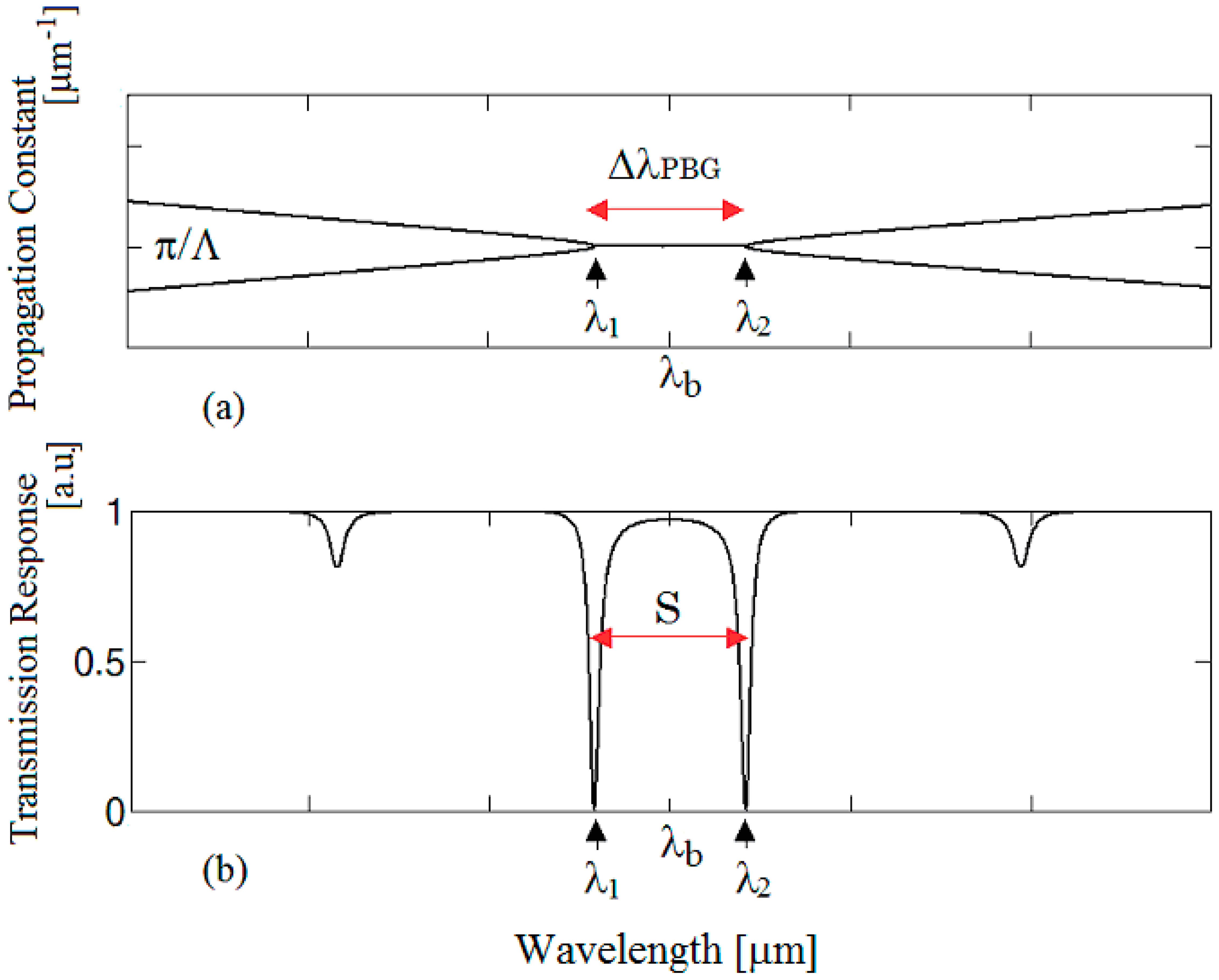
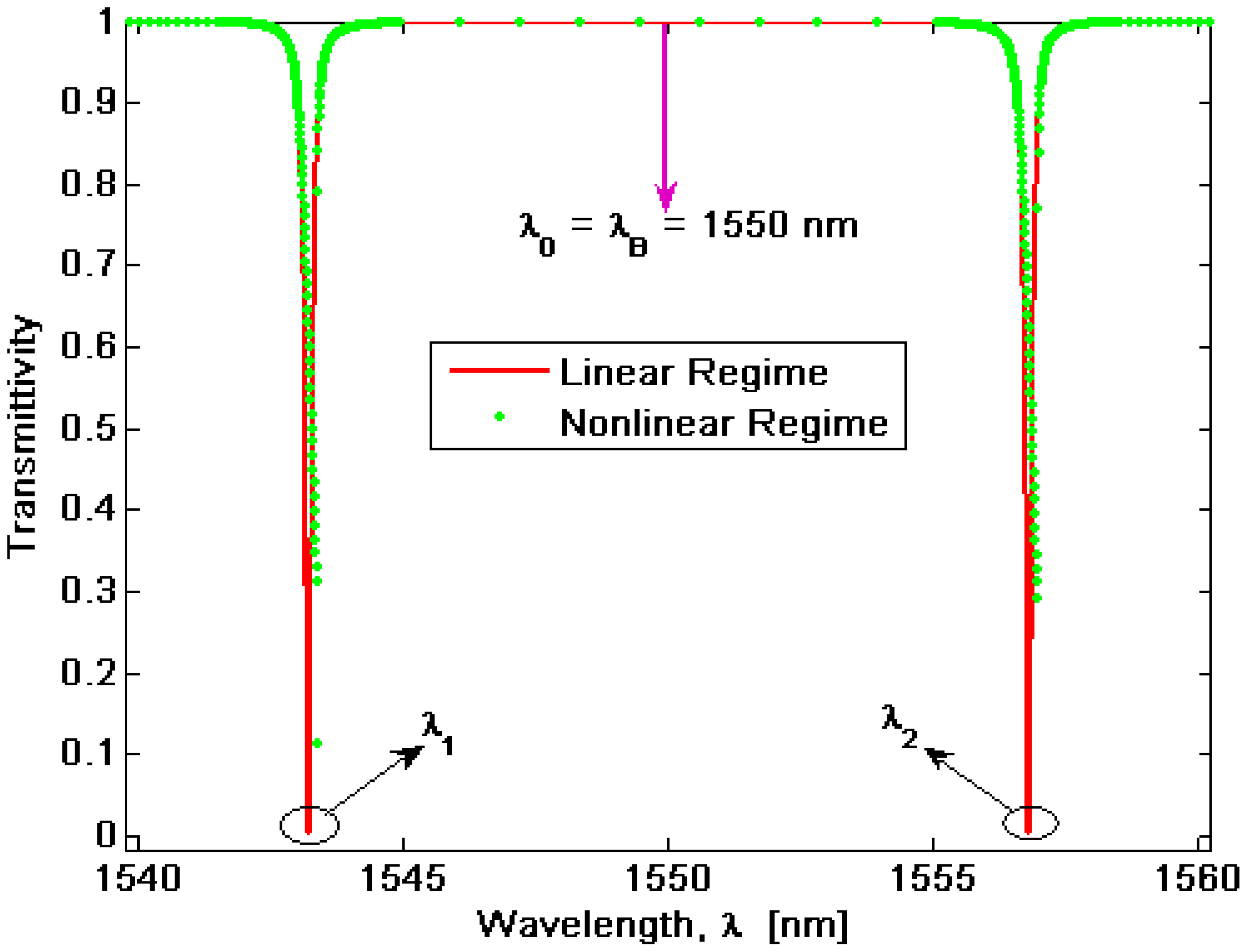
Before describing the general mathematical model to include the nonlinear effects, it is needed to outline the basics of the BMR device. Its physical behavior and the theoretical model in linear regime have been experimentally proven in case of a Bragg grating included in a fiber ring resonator [10]. In fact, if the input wave (Sp) has a wavelength close to Bragg wavelength (λb = 2neffΛ), two counter-propagating beams, coupled to each other, are originated inside the optical microcavity. This coupling, in its turn, induces two split resonances at λ1 and λ2 as in Figure 2b. In addition, the splitting magnitude can be directly evaluated as:
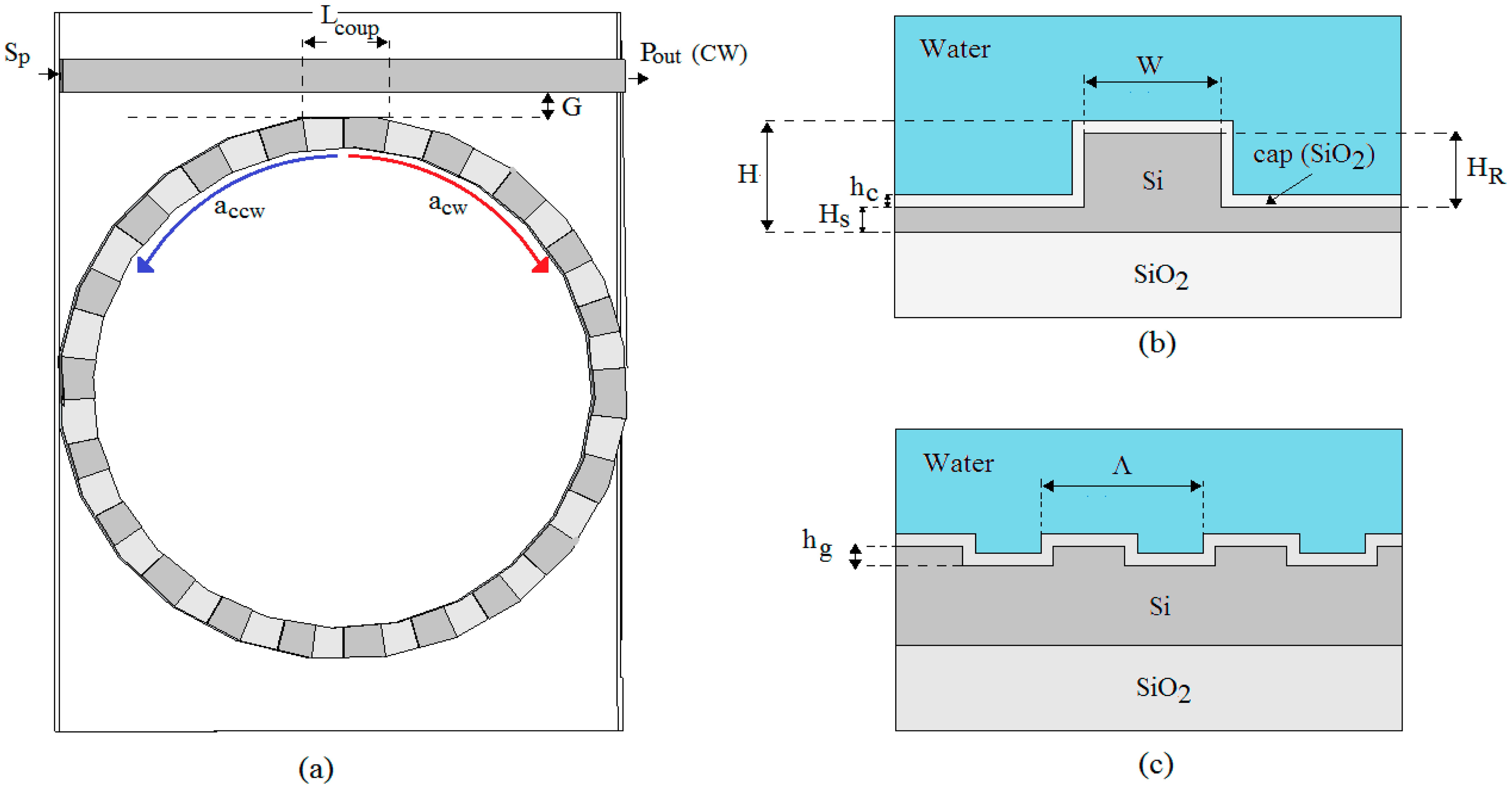
To clarify this mode splitting, we report the eigenvalues of Bragg grating in Figure 2a and the BMR spectral response in Figure 2b. As evidenced by Equations (1) and (2), if the Bragg grating period varies, both the cavity length and the Bragg wavelength will change, inducing a shift of the split dips. However, their distance still remains constant because the PBG extension remains almost unvaried. In fact, as reported in Figure 3, if Λ is changed to 1 × 10⁻² μm, λb passes from λb(α) to λb(β) and the splitting ΔλPBG(α) keeps a constant magnitude.
This effect means that the device becomes almost insensitive to the length variations, associated with fabrication tolerances as experimentally proven in [14], but also to the environmental perturbations [10]. Once the splitting nature has been explained by focusing also on the advantage in terms of fabrication tolerances and insensitivity to environmental perturbations, we analyze the operation of the device when the non-linear effects are excited to investigate if potential performance improvements can be achieved. To this aim, a model based on a set of partial differential equations for the nonlinear coupling between clockwise (CW) and counter-clockwise (CCW) waves inside the BMR has been developed, including one rate equation for the hole-electron pairs generated in the resonator by the TPA effect as induced by the propagating waves.
The equations have been derived assuming the input pump (Sp) as injected in the BMR by means of the evanescent coupling between the resonant microcavity and the input external bus, both based on rib waveguides in SOI technology platform. G and Lcoup are the directional coupler gap and length, respectively. Although the microcavity in Figure 1a is a ring resonator, the following model can be applied to any microcavity shape, such as race-track, ring or disk resonators. The cross-section of the not-etched section waveguide is sketched in Figure 1b, showing the main geometrical parameters such as the rib etch depth HR and width W, the overall waveguide height H, and the slab height HS. In addition, the optical device can be covered by water solution, as in Figure 1b. Finally, a SiO2 protective passivation layer has been also included in the waveguide cross section.
Without any lack of generality, we assume that the electric field inside the microcavity is predominantly a single transverse mode (single-mode condition). Thus, up to two propagating modes are assumed in the resonator, one quasi-TE (dominant horizontal x-component of electric field) and one quasi-TM (dominant vertical y-component), where x and y designate the waveguide cross section coordinates. Hereinafter, the input pump wave (Sp) is aligned with quasi-TE or quasi-TM polarization. Thus, according to the full-vectorial nonlinear coupled mode theory [15], the equations describing the power transfer among the CW and CCW waves can be respectively written as:
Furthermore, in Equations (3) and (4), the terms βi,ψTPA(T) (I = CW,CCW) represent the TPA effect on the ith beam induced by the ψth wave (ψ = CW,CCW). Moreover, the coefficient γ(T) = n2(T)ω/c takes into account the SPM and XPM effects as induced by Kerr nonlinearity. Finally, we have also included in the model the thermal dependence for the coefficients βi,ψTPA(T), and n2(T) by considering the equations proposed in [16], thus realising a fully self-consistent approach. The effective modal area relevant to the ith wave (i = CW,CCW) plays a fundamental role since it determines the efficiency with which any nonlinear effect manifests inside the optical SOI waveguide. According to the full-vectorial coupled mode theory [15], the effective modal areas are calculated as:
As mentioned before, the proposed model includes the temperature and waveguide mechanical stress parameters in order to evaluate thermal and stress influence on the sensor performance. Thus, generally speaking, a thermal difference with respect to a reference temperature (Tref) induces strain and stress fields inside the optical waveguide, which are related as [18]:
3. Results and Discussion
3.1. Physical Analysis
In this sub-section, a number of parametric simulations are proposed in order to find the physical features of BMR operating in linear and nonlinear regimes. In this context, it is worth describing briefly the procedure for the spectra calculations based on the model presented in the previous section. With the aim to realize self-consistent simulations, we have implemented an integrated algorithmic procedure based on both hand-made code and commercial software based on full-vectorial finite-element method (FEM) [19]. Consequently, we determine firstly the stress field in the waveguide for a fixed temperature value by solving numerically Equation (10) by FEM. It solves the static equilibrium equation, simultaneously satisfying the stress–strain relation, the thermal effects and the strain–displacement relation, with proper boundary conditions for the displacement variables in the x, y, and z directions. Once the stress distribution in the vicinity of the ridge waveguide has been calculated, the local refractive index distribution can be evaluated using Equation (11), and then FEM is used to solve the Maxwell's equations and determine the optical mode distributions and effective refractive index for both quasi-TE and quasi-TM polarizations at the operative wavelengths. It is worth outlining that the FEM electromagnetic module used in this step works together with the FEM stress module in order to take into account the stress effect on the material refractive index. Now, the electric-field distributions are used to calculate the grating coupling coefficient and the nonlinear effective modal area using Equations (5) and (8), respectively. Finally the hand-made code, solving the equations system (3), (4) and (9), allows the spectra for CW and CCW waves to be accurately evaluated.
In conclusion, the procedure described above gives the BMR features in both linear and nonlinear regimes, following an approach simultaneously integrated and multi-physics. Hereinafter, the simulations have been performed by setting typical physical parameters and waveguide geometry for silicon-based technology, as listed in Tables 1 and 2. According to Figure 1a, the transmittivity is defined as:
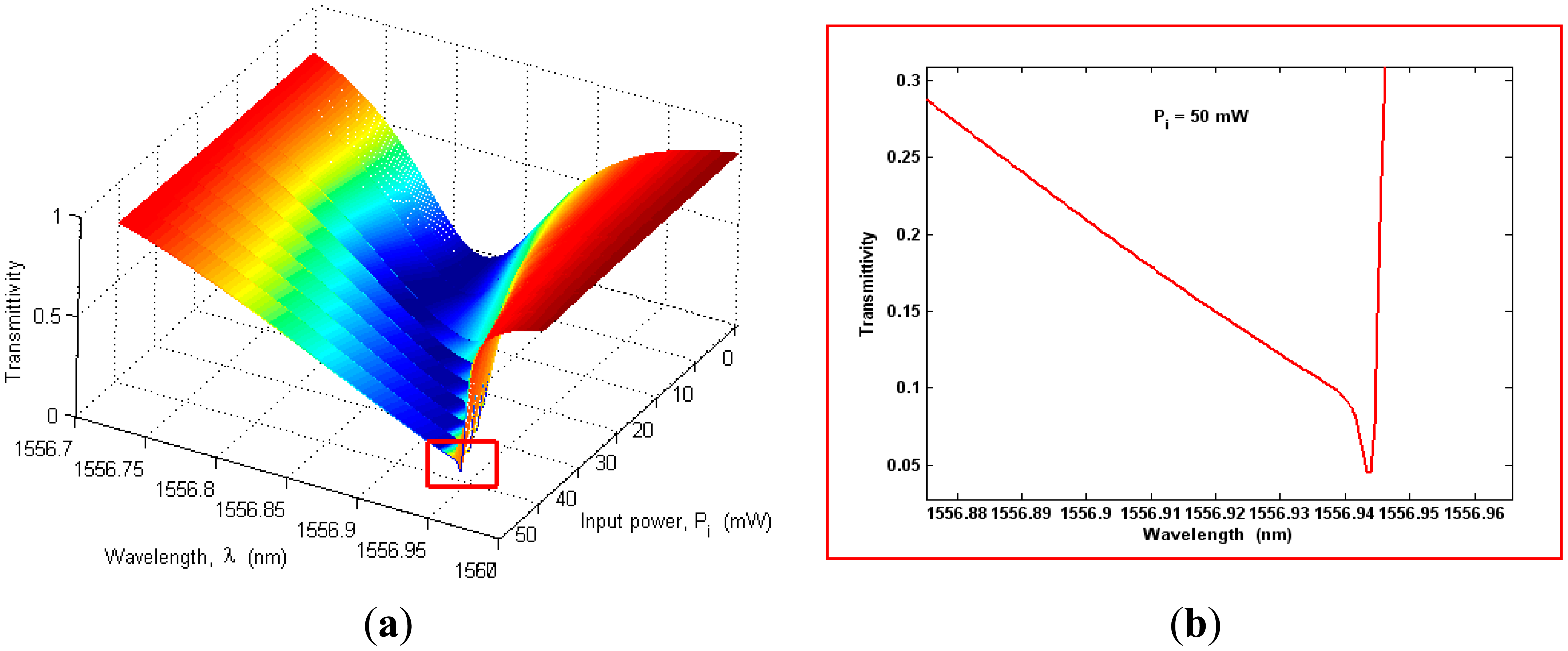
In Figure 4 the transmittivity is shown as a function of different values of input power. In the simulations, we have assumed a grating period of Λ ≅ 245.4 nm in order to satisfy the Bragg condition at λB = 1550 nm, a cavity length Lcavity = 92.28 μm corresponding to a period number Nperiod = 376, σi = −100 MPa, and T = Tref = 293 K.
About the initial stress σi, we have introduced the external parameter σi, defined as the in-plane stress component present in the uniform SiO2 upper cap film, far away from the ridge. In this work, the stress in the protective oxide layer induced by fabrication processes has been considered as well. Alternatively, the stress in the cap material can be altered by thermal anneals, typically assuming values ranging from −400 MPa to −100 MPa. The plot in Figure 4 clearly shows the resonance splitting effect, previously described in Section 2. The grating presence induces a coupling effect between CW and CCW waves, resulting in a split doublet with resonances placed at λ1 = 1543.23 nm and λ2 = 1556.82 nm, respectively.
In particular, for input powers lower than 2 mW (linear regime), both wavelengths λ1 and λ2 exclusively depend on the coefficient μ(T,σ) as well as on the decay time, according to:
Moreover, if the grating coupling coefficient is much larger than the photon decay rate, Equation (13) can be approximated by means of the relationship ω1,2 ≅ ω0 ± μ(T,σ), but only in linear regime. In fact, as shown in Figure 4, by increasing the input power the transmittivity exhibits both a shift towards higher wavelengths and a spread of the resonance shape as induced by nonlinear effects. This is evidenced in Figure 5, where a zoom plot is shown around λ2 as in Figure 5b. Therefore, Figure 5a,b clearly indicates that the nonlinear effects act by deforming the spectrum shape with respect to the Lorentzian profile, typical of the linear regime. Moreover, the degree of the deformation increases by increasing the input power. In addition, a very specific feature can be also observed for input powers larger than a threshold value, hereinafter indicated as P̅ι, depending on the microcavity parameters (in particular, on the cavity quality factor).
In fact, for Pi ≥ P̅ι the transmittivity spectrum, even if totally deformed, presents a very narrow, shaped and deep spike, as evidenced in Figure 5b. This spike can be very useful to improve the sensor performance with respect to the linear regime, as it will be demonstrated in the next section.
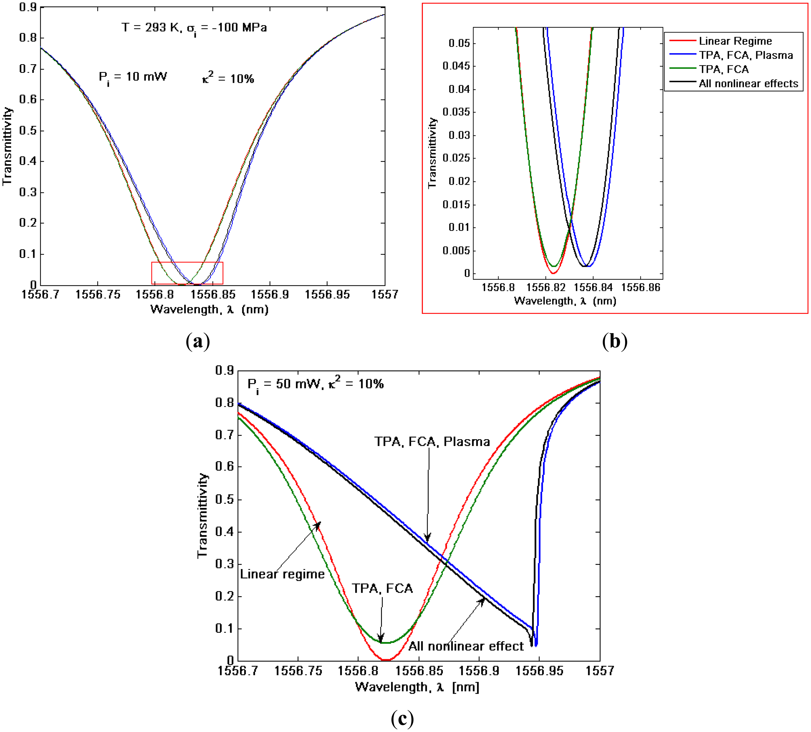
However, at this step, it is worth finding the physical reasons for the spike formation and we can refer to Figure 6a,b, where the transmittivity spectrum is shown in presence of nonlinear effects acting separately for Pi = 10mW ≤ P̄ι and Pi = 50 mW ≥ P̄ι, respectively. In this context, Figure 6 shows how the only presence of both TPA effect with induced FCA and plasma dispersion effects (blue curve) induce similar spectrum features with respect to the real case (black curve), but with a shift in the spike position. This offset is induced by the absence of the shift effect towards shorter wavelengths, depending on the Kerr effect. Moreover, by neglecting the TPA-induced plasma dispersion effect (see green curve), the transmittivity evidences only a spread with respect to the linear regime (red curve), without any wavelength shift. Therefore, with respect to the linear regime the resonance wavelength shift is determined by the competition between opposite trends as induced by Kerr and plasma dispersion effect, with a strength depending on the input power, as sketched in Figure 6b,c. Finally, we conclude that the spike formation can manifest only under the condition Pi ≥ P̄ι, where a strong TPA effect, a not negligible spectrum red shift as induced by the high plasma dispersion effect as well as a higher FCA for wavelengths shorter than the spike wavelength, simultaneously occur and can be observed.
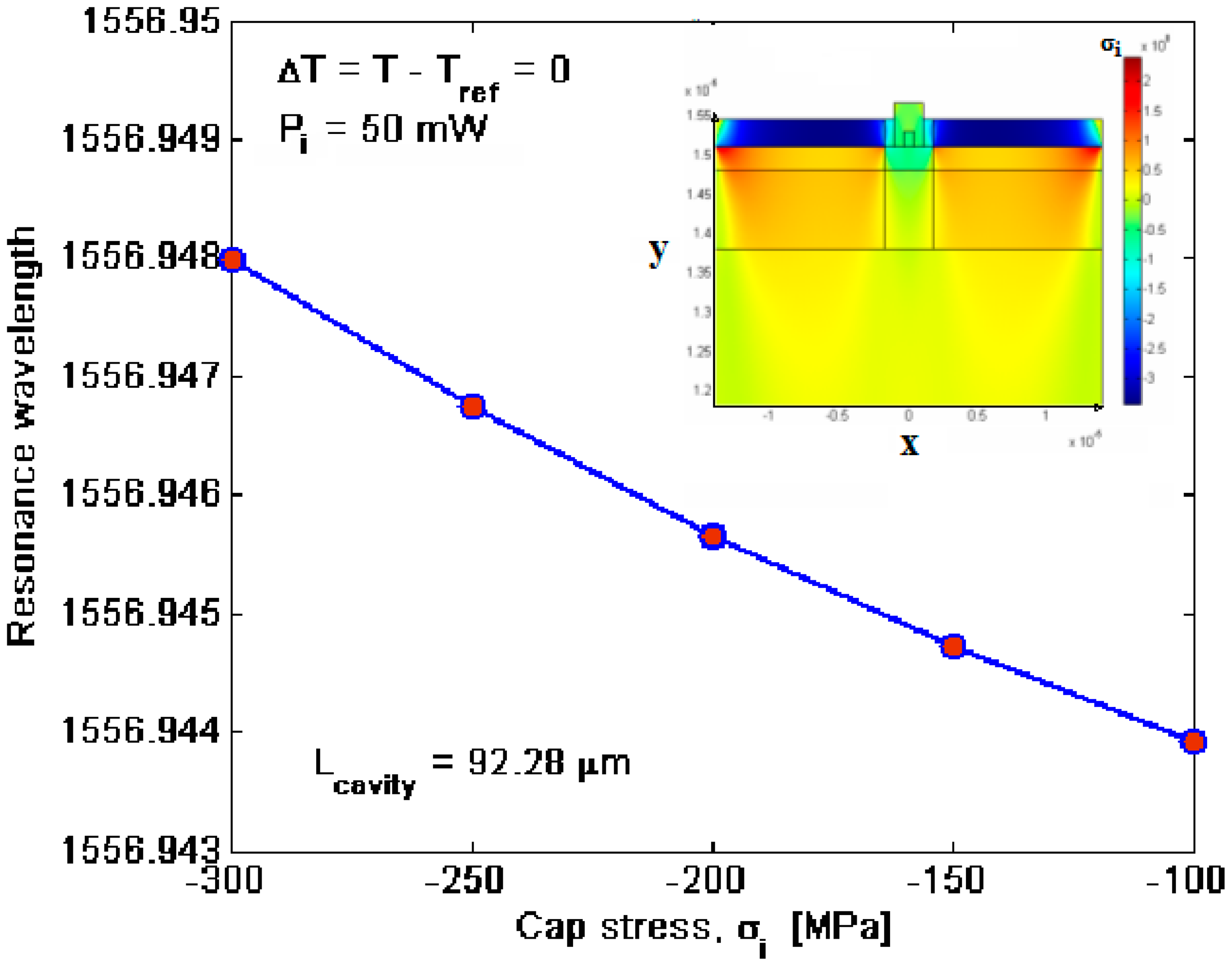
In addition, for Pi < P̄ι the nonlinear effects only determine an increasing of optical losses due to TPA and FCA, being the plasma dispersion effect too weak to induce a sufficient red shift and, then, to produce the spike formation. In the following, we propose a number of parametric simulations to find both the stress and thermal influences. To this purpose, we show in Figure 7 the stress field inside the not etched cross section waveguide obtained by means of FEM simulations and induced only by the stress localized in the oxide cap layer. In particular, we have assumed Pi = 50 mW, σi = −400 MPa and T = Tref = 293 K. In addition, the spectral shift has been estimated as a function of the cap stress, as shown in Figure 7. Thus, by increasing the module of the cap stress σi, the resonance wavelength shift towards higher values with a slope of −2.3121 × 10⁻⁵ nm/MPa. In any case, this shift cannot be considered as a detrimental effect. In fact, since the σi value depends on the fabrication processing and annealing, it can be considered as known and constant.
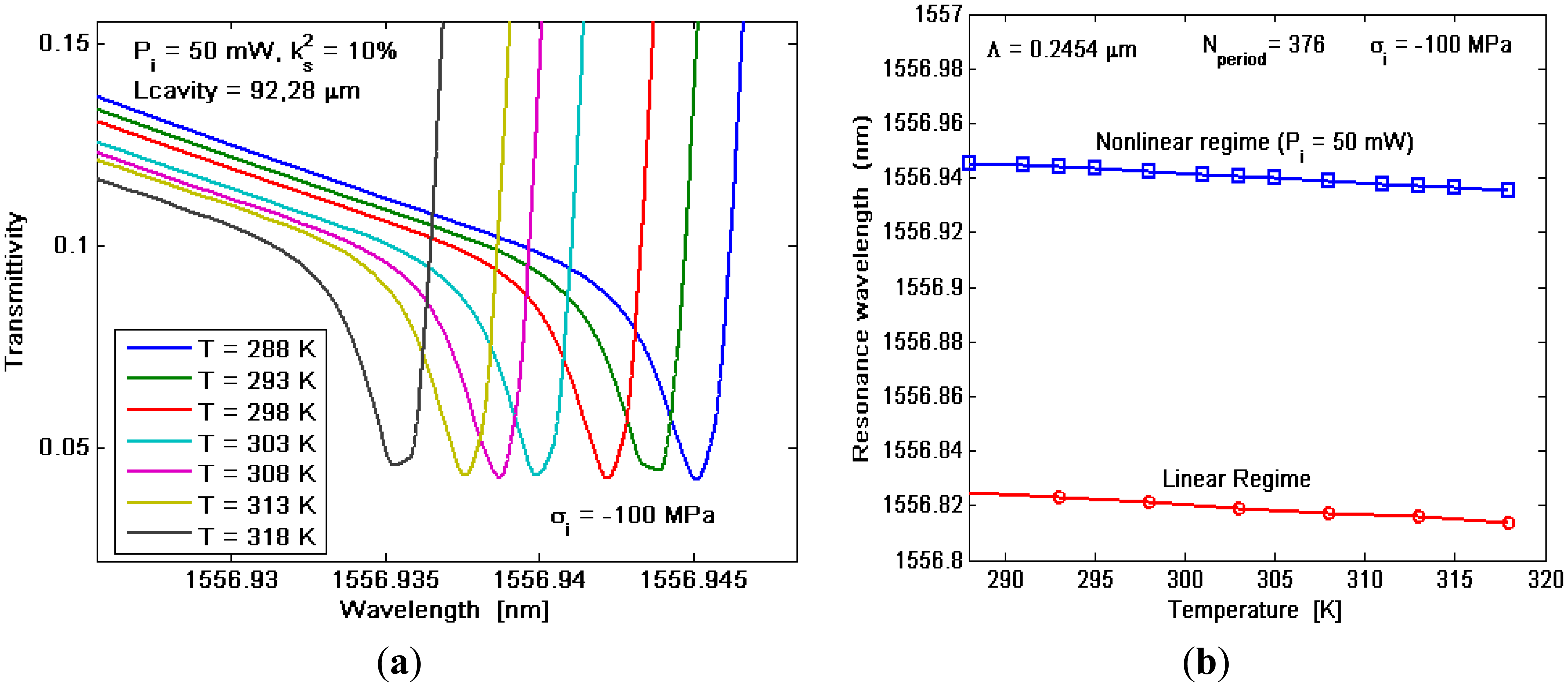
Thus, evaluation of σi and curve in Figure 7 lead us to well determine the exact resonance wavelength, since the curve can be used to set the sensor when σi is already known. On the contrary, thermal changes introduce not negligible effects as indicated in Figure 8, where the transmittivity spectrum around λ2 is shown for different values of the temperature T.
The simulations plotted in Figure 8a,b have been obtained by assuming Pi = 50 mW, σi = −100 MPa, Λ ≅ 245.4 nm, and Lcavity = 92.28 μm (Nperiod = 376). In particular, Figure 8a indicates that, by increasing the temperature, the transmittivity suffers from a high shift towards higher wavelengths. In fact, by considering ΔT = T − Tref ≠ 0, the thermal effects manifest either a change in the silicon refractive index or, according to Equation (10), a variation in the stress field inside the waveguide cross section with respect to the effect induced by σi. In summary, the resonance wavelength shift as a function of the temperature, as in Figure 8b, could assume values sufficiently high to represent a detrimental effect and compromise the sensor sensitivity, as it will be demonstrated in the following.
3.2. Sensor Performance
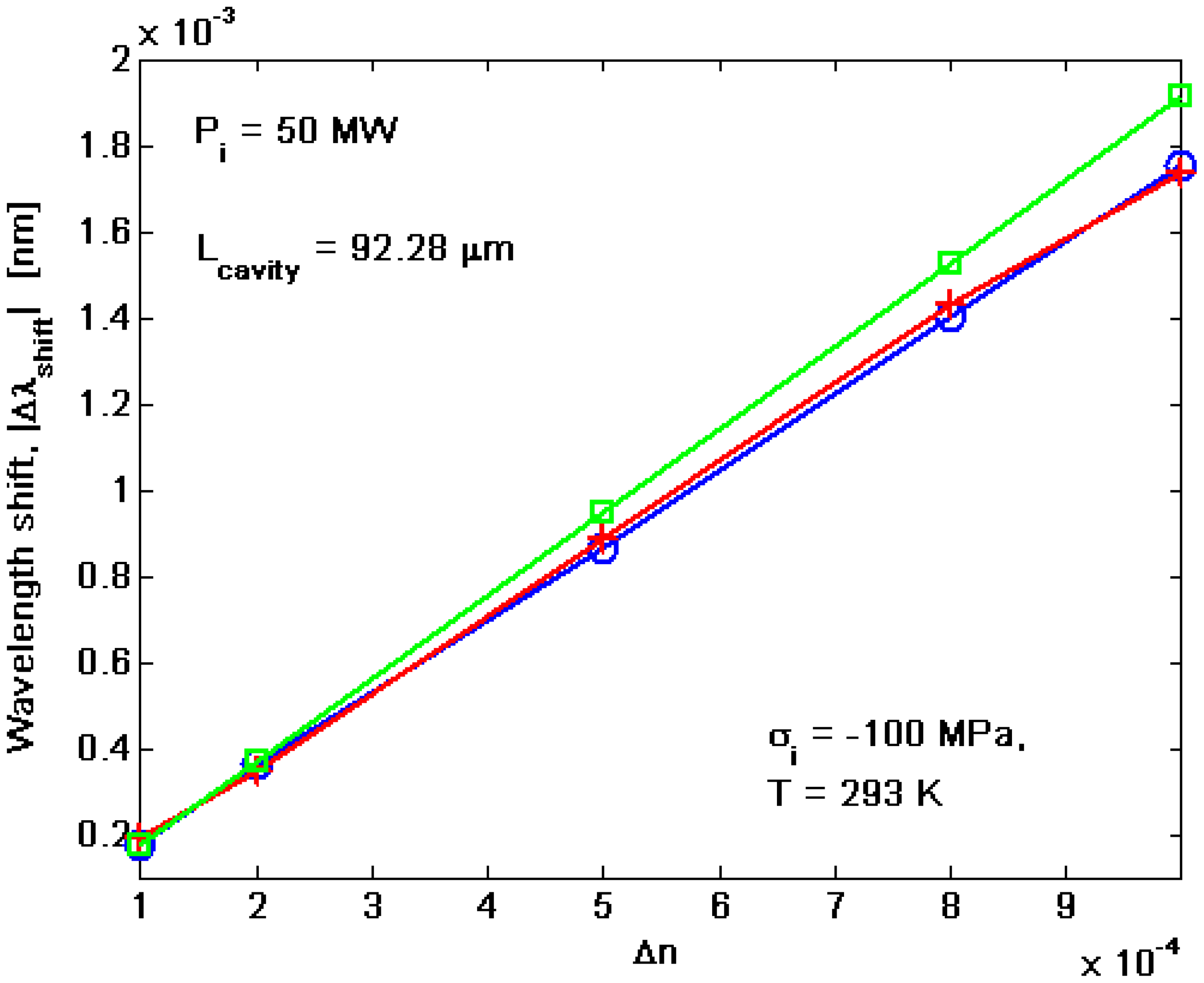
The goal of this sub-section is to analyze the sensor performance in both linear and nonlinear regimes. We have performed a number of parametric simulations according to the integrated and multi-physics algorithm described in previous sections, in order to investigate the performance of the SOI Bragg microcavity resonator. In this sense, by assuming that the cover medium (i.e., water solution) refractive index changes as a function of the concentration of the element to be detected, diluted into the cladding solution, the BMR sensor sensitivity can be written as:
It is worth outlining that the wavelength shift |Δλshift| has been evaluated as the resonance wavelength shifts with respect to the rest condition of the sensor: Δn = 0, and T = Tref = 293 K. In the simulations, Pi = 50 mW, σi = − 100 MPa, T =Tref, Λ ≅ 245.4 nm, and Lcavity = 92.28 μm (Nperiod = 376) are assumed. The linear profile gives a sensitivity of about 1.7 nm/RIU for each resonant mode of the split doublet. However, as outlined in Figure 8, the temperature changes induce a strong shift of the resonance wavelength. Thus, the sensitivity is limited by the temperature influence, too. Therefore, we can refer to Figure 10 in order to estimate the conditions for a temperature control. The straight line represents the thermal-induced resonance wavelength shift evaluated with respect to the room temperature (Tref = 293 K) and Δn = 0. On the contrary, the horizontal lines indicate the resonance wavelength shift, Δλshift, calculated at T = Tref = 293K for different values of Δn.
Thus, the intersection points represent the temperature change values with respect to Tref inducing, in absence of the element in the cladding solution, the same wavelength shift produced by Δn value related to the horizontal line intercepted. For example, a temperature change T – Tref = 0.54 °C induces the same wavelength shift of Δn = 10−4 at Tref. Consequently, to detect an element concentration change that produces a cladding refractive index change lower than 10−4, it is needed to control and keep constant the sensor temperature with great accuracy, within 0.54 °C.
Performance of integrated optical sensors based on Bragg microcavity resonator depends not only on Sr but also on their resolution or detection of level (DoL), defined as the minimum detectable change in resonance wavelength. In the Lorentzian resonance shape, this quantity essentially depends on the Full-Width-Half-Maximum (δλFWHM) value. In our case, this is true in linear regime or nonlinear regime with Pi < P̄ι. On the contrary, for Pi ≥ P̄ι the sensor resolution depends on the separation of very shaped and narrow resonance spikes. It is worth outlining that, under the condition Pi ≥ P̄ι, we can exploit two advantages with respect to the simple ring resonator configuration, without any Bragg grating. In fact, by designing the BMR in SOI technology, it is possible to reduce the cavity resonance linewidth due to the strong structural dispersion that occurs around the PBG edges [20]. An additional improvement is realized using the nonlinearity-induced spike formation. In Figure 11, the sensor resolution (|Δλres|) is shown as a function of the input power for different coupling coefficients. Due to the complexity of the mathematical model proposed, which includes nonlinear, thermal and stress effects, it is not possible to derive a closed-form relationship to calculate |Δλres|), then the curves have been obtained numerically by evaluating the minimum shift acceptable in order to well discriminate the resonance spectrum, following the “Sparrow” criterion. In the simulations, we have assumed σi = −100 MPa, T = Tref, Λ ≅ 245.4 nm, and Lcavity = 92.28 μm (Nperiod = 376). Consequently, once κ2 has been fixed, |Δλres| is shown to increase with increasing the input power up to values where the non linear effects are dominant, giving an abrupt drop of the curve.
Thus, for Pi < P̄ι, (linear regime) the best sensor performance in terms of resolution can be obtained for lower input powers. In fact, under this condition an increase in power only induces an increase in the losses (TPA and FCA), with consequent spread of the resonance Lorentzian shape. The case with P < P̄ι is very different, giving a strong improvement of |Δλres| which is related to the formation of the very narrow spike in the transmittivity spectrum. In addition, the plot shows that, for a given input power, the sensor resolution increases with decreasing κ2, due to the increment of the microcavity quality factor. Moreover, if the microcavity quality factor increases as well as the enhancement of the resonator, the threshold of nonlinear effects is reduced and, then, the value of P̄ι decreases by decreasing κ2 (so inducing the abrupt drop of the curves). The main values of sensor resolution (or detection of level) are listed in Table 3 in both operation regimes. It is worth outlining that the curves obtained in Figure 11 under-estimate the resolution, considering it as resolved to Lorentzian profiles (as in our case for Pi < P̄ι) for a separation equal to δλFWHM/3, according to the Sparrow criterion. In this context, by comparing Figure 9 and Table 3, the proposed sensor based on Bragg microcavity resonator can detect cover RI changes as low as Δn ≅ 8 × 10⁻⁴, operating in non-linear regime with Pi ≥ 9.86 mW, Lcavity = 92.28 μm, and κ2 = 3%. However, using the indications proposed in [21] in which two resonance profiles are considered as resolved if they are separated by δλFWHM/10 and by appropriately scaling the curves of Figure 11, the proposed sensor can detect a refractive index variation Δn ≅ 1 × 10⁻⁴ RIU in the same operation conditions. This means that the non-linear regime can effectively improve the sensor performance in terms of sensor resolution of at least one order of magnitude (still not using optimal parameters and depending on the coupling coefficient for the given parameters), opening an unexplored approach to RI optical sensing. Moreover, we would underline that, although the obtained DoL results are not to be improved with respect to the best values reported in the literature for RI optical sensors (i.e., Δn < 1 × 10⁻⁶ [22]), the advantages arising from the split mode structure, consisting in good immunity to the fabrication tolerances and the environmental perturbations, are preserved by operating in a non-linear regime, which is of great importance in RI optical sensing applications.
The proposed approach can be used in spectroscopic differential systems, where the common optical noise of the two resonant split modes can be suppressed.
4. Conclusions
In this paper, the physics and the operation of a SOI Bragg grating ring resonator have been investigated as a photonic sensing approach working in both linear and non-linear regimes. The model takes into account all the non-linear effects and optical losses, as well as the thermal and stress influence, too. In linear regime, the device shows a spectral response characterized by a photonic band gap (PBG) behavior. Very close to the band gap edges, it exhibits split resonant modes induced by the grating effect and having a splitting magnitude equal to the PBG spectral extension, almost insensitive to both fabrication tolerances and environmental perturbations. When this device operates in a non-linear regime, exactly in that spectral region showing the split resonant mode structure, our integrated and multi-physics algorithm allows to estimate, in a self-consistent way, the improvement of sensor performance as well as the thermal and stress-induced resonance shift and, then, the sensor temperature control as well. Then, a number of numerical simulations are presented in order to estimate sensor sensitivity and resolution. These simulations confirm that, with respect to the linear regime, the resolution can be improved in a non-linear regime by exploiting the spectral spikes arising from a specific combination of the non-linear effects involved in the sensor architecture. Moreover, the detection of the variation of the distance between the two split modes (i.e., the two spikes generated in non linear regime) allows a spectroscopic differential system to be achieved, in which the common noise, acting on the two split modes, can be easily suppressed. These conclusions will be of great importance in realizing miniaturized linear and non-linear spectroscopic optical sensors, especially in SOI technology platforms, to be used for high performance chemical, biochemical and biological sensing applications.
Author Contributions
In this work, the general conception has been developed by F. De Leonardis, C.E. Campanella and V.M.N. Passaro, while the model has been developed by F. De Leonardis and B. Troia. Moreover, V.M.N. Passaro has prepared the final draft and A.G. Perri has guaranteed the critical reading.
Conflicts of Interest
The authors declare no conflict of interest.
References
- Hausmann, B.J.M.; Shields, B.; Quan, Q.; Maletinsky, P.; McCutcheon, M.; Choy, J.T.; Babinec, T.M.; Kubanek, A.; Yacoby, A.; Lukin, M.D.; et al. Integrated Diamond Networks for Quantum Nanophotonics. Nano Lett. 2012, 12, 1578–1582. [Google Scholar]
- Kippenberg, T.J.; Vahala, K.J. Cavity Optomechanics: Back-Action at the Mesoscale. Science 2008, 321, 1172–1176. [Google Scholar]
- Kippenberg, T.J.; Holzwarth, R.; Diddams, S.A. Microresonator Based Optical Frequency Combs. Science 2011, 332, 555–559. [Google Scholar]
- Chao, C.; Guo, L.J. Biochemical sensors based on polymer microrings with sharp asymmetrical resonance. Appl. Phys. Lett. 2003, 83, 1527–1529. [Google Scholar]
- Passaro, V.M.N.; de Tullio, C.; Troia, B.; La Notte, M.; Giannoccaro, G.; de Leonardis, F. Recent Advances in Integrated Photonic Sensors. Sensors 2012, 12, 15558–15598. [Google Scholar]
- La Notte, M.; Troia, B.; Muciaccia, T.; Campanella, C.E.; de Leonardis, F.; Passaro, V.M.N. Recent Advances in Gas and Chemical Detection by Vernier Effect-Based Photonic Sensors. Sensors 2014, 14, 4831–4855. [Google Scholar]
- Campanella, C.E.; Campanella, C.M.; de Leonardis, F.; Passaro, V.M.N. A high efficiency label-free photonic biosensor based on vertically stacked ring resonators. Eur. Phys. J. Spec. Top. 2014, 223. [Google Scholar]
- Zhu, J.; Ozdemir, S.K.; Xiao, Y.F.; Li, L.; He, L.; Chen, D.R.; Yang, L. On-chip single nanoparticle detection and sizing by mode splitting in an ultrahigh-Q microresonator. Nat. Photonics 2010, 4, 46–49. [Google Scholar]
- Li, M.; Wu, X.; Liu, L.; Fan, X.; Xu, L. Self-Referencing Optofluidic Ring Resonator Sensor for Highly Sensitive Biomolecular Detection. Anal. Chem. 2013, 85, 9328–9332. [Google Scholar]
- Campanella, C.E.; Giorgini, A.; Avino, S.; Malara, P.; Zullo, R.; Gagliardi, G.; de Natale, P. Localized strain sensing with fiber Bragg-grating ring cavities. Opt. Express 2013, 21, 29435–29441. [Google Scholar]
- Bowers, J.; Liang, D.; Fang, A.; Park, H.; Jones, R.; Paniccia, M. Hybrid Silicon Lasers. The Final Frontier to Integrated Computing. Opt. Photonics News 2010, 21, 28–33. [Google Scholar]
- Reed, G.T. The optical age of silicon. Nature 2004, 427, 595–596. [Google Scholar]
- Pavesi, L. Will silicon be the photonic material of the third millennium? J. Phys. Condens. Matter. 2003, 15, R1169–R1196. [Google Scholar]
- Ramos, C.A.; Morichetti, F.; Moñux, A.O.; Fernández, I.M.; Strain, M.J.; Melloni, A. Dual-Mode Coupled-Resonator Integrated Optical Filters. IEEE Photon. Technol. Lett. 2014, 26, 929–932. [Google Scholar]
- De Leonardis, F.; Troia, B.; Passaro, V.M.N. Design Rules for Raman Lasers Based on SOI Racetrack Resonators. IEEE Photonics J. 2013, 6. art. 6648677. [Google Scholar]
- Dinu, M. Dispersion Phonon-Assisted Nonresonant Third-Order Nonlinearities. IEEE J. Quantum Electron. 2003, 39, 1498–1503. [Google Scholar]
- Li, H.H. Refractive Index of Silicon and Germanium and Its Wavelength Temperature Derivatives. J. Phys. Chem. Ref. Data 1980, 9, 560–658. [Google Scholar]
- Ye, W.N.; Xu, D.X.; Janz, S.; Chaben, P.; Picard, M.J.; Lamontagne, B.; Tarr, N.G. Birefringence Control Using Stress Engineering in Silicon-on-Insulator (SOI) Waveguides. J. Light. Technol. 2005, 23, 1308–1318. [Google Scholar]
- Comsol Multiphysics; ver. 3.2; Single License, COMSOL Inc.: Stockholm, Sweden, 2005.
- Goldring, D.; Levy, U.; Mendlovic, D. Highly dispersive micro-ring resonator based on one dimensional photonic crystal waveguide design and analysis. Opt. Express 2007, 15, 3156–3168. [Google Scholar]
- De Vos, K.; Bertolozzi, I.; Bienstman, P.; Baets, R.; Schacht, E. Optical Biosensor based on Silicon-on-Insulator Microring Resonators for Specific Protein Binding Detection. Proceedings of the Symposium IEEE/LEOS Benelux Chapter, Eindhoven, The Netherlands, 30 November–1 December; 2006; pp. 213–216. [Google Scholar]
- Nemova, G.; Kabashin, A.V.; Kashyap, R. Surface plasmon-polariton Mach-Zehnder refractive index sensor. J. Opt. Soc. Am. B 2008, 25, 1673–1677. [Google Scholar]


| Parameters | Assumed Values |
|---|---|
| EY (Si) | 130 (GPa) |
| EY (SiO2) | 76.7 (GPa) |
| ν (Si) | 0.27 |
| ν (SiO2) | 0.186 |
| αtherm (Si) at 293 K | 3.6 × 10⁻⁶ (K−1) |
| αtherm (SiO2) at 293 K | 5.4 × 10⁻⁷ (K−1) |
| p11 (Si) | −0.101 |
| p12 (Si) | 0.0094 |
| p11 (SiO2) | 0.16 |
| p12 (SiO2) | 0.27 |
| αlass | 0.5 dB/cm |
| τeff | 1 ns |
| Nc0 | 1020 (m−3) |
| Parameters | Assumed Values |
|---|---|
| Duty cycle | 50% |
| hg | 50 nm |
| H | 450 nm |
| HR | 150 nm |
| HS | 300 nm |
| W | 700 nm |
| hc | 350 nm |
| Parameters | Values | ||
|---|---|---|---|
| Coupling factors (κ2(T,σ)) | 3% | 5% | 10% |
| |Δλres| at Pi = 1 mW(Linear regime) | 26 pm | 40 pm | 48 pm |
| P̄ι | 9.86 mW | 13 mW | 35.47 mW |
| |Δλres| for Pi ≥ P̄ι (Non-linear regime) | 1.7 pm | 2.1 pm | 3 pm |
© 2014 by the authors; licensee MDPI, Basel, Switzerland. This article is an open access article distributed under the terms and conditions of the Creative Commons Attribution license ( http://creativecommons.org/licenses/by/3.0/).
Share and Cite
De Leonardis, F.; Campanella, C.E.; Troia, B.; Perri, A.G.; Passaro, V.M.N. Performance of SOI Bragg Grating Ring Resonator for Nonlinear Sensing Applications. Sensors 2014, 14, 16017-16034. https://doi.org/10.3390/s140916017
De Leonardis F, Campanella CE, Troia B, Perri AG, Passaro VMN. Performance of SOI Bragg Grating Ring Resonator for Nonlinear Sensing Applications. Sensors. 2014; 14(9):16017-16034. https://doi.org/10.3390/s140916017
Chicago/Turabian StyleDe Leonardis, Francesco, Carlo Edoardo Campanella, Benedetto Troia, Anna Gina Perri, and Vittorio M. N. Passaro. 2014. "Performance of SOI Bragg Grating Ring Resonator for Nonlinear Sensing Applications" Sensors 14, no. 9: 16017-16034. https://doi.org/10.3390/s140916017
APA StyleDe Leonardis, F., Campanella, C. E., Troia, B., Perri, A. G., & Passaro, V. M. N. (2014). Performance of SOI Bragg Grating Ring Resonator for Nonlinear Sensing Applications. Sensors, 14(9), 16017-16034. https://doi.org/10.3390/s140916017