Metal-Insulator-Semiconductor Photodetectors


Abstract
:1. Introduction
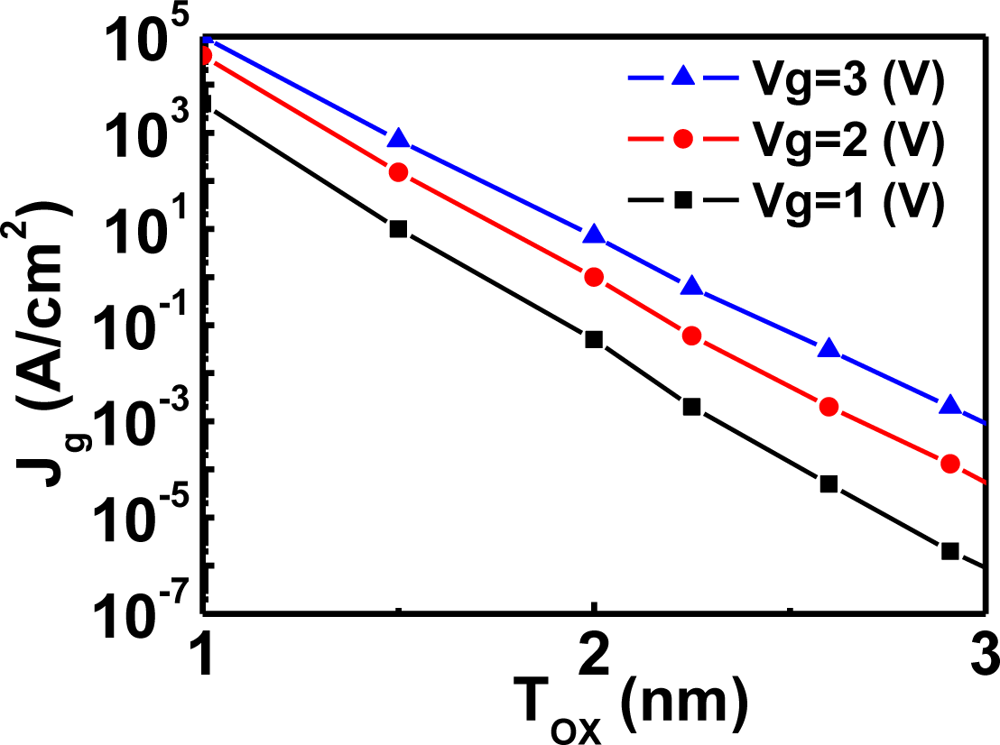
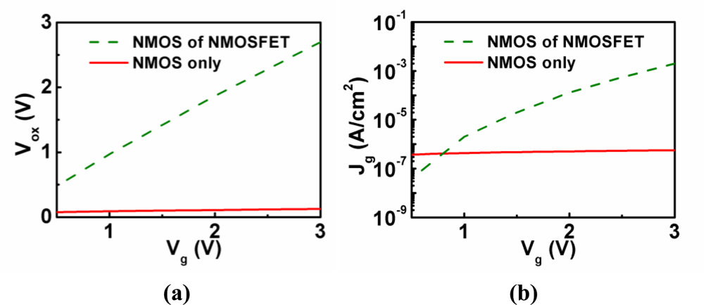
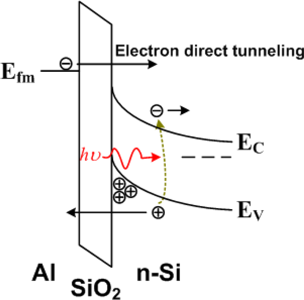
2. Electrical Characteristics of MIS Structures
| A, B, D, and α | model parameters; |
| Tox | oxide thickness; |
| Vox | oxide voltage; |
| φb0 | semiconductor/oxide barrier height; |
| φb | actual tunneling barrier height; |
| Vth | threshold voltage. |
3. MIS UV Photodetectors
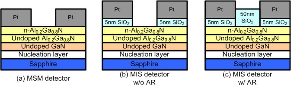
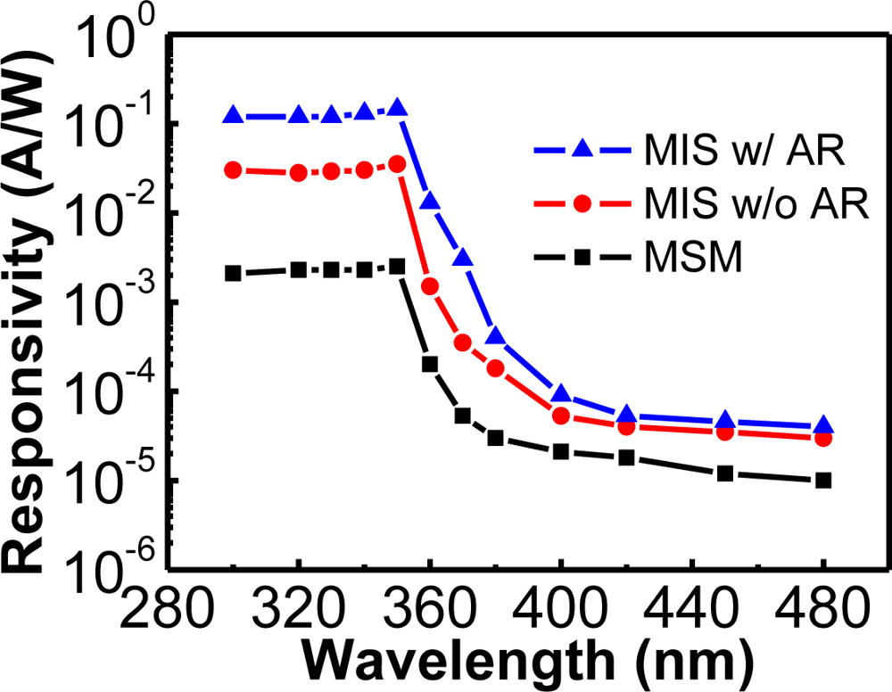
3.1. III–V MIS UV Photodetectors
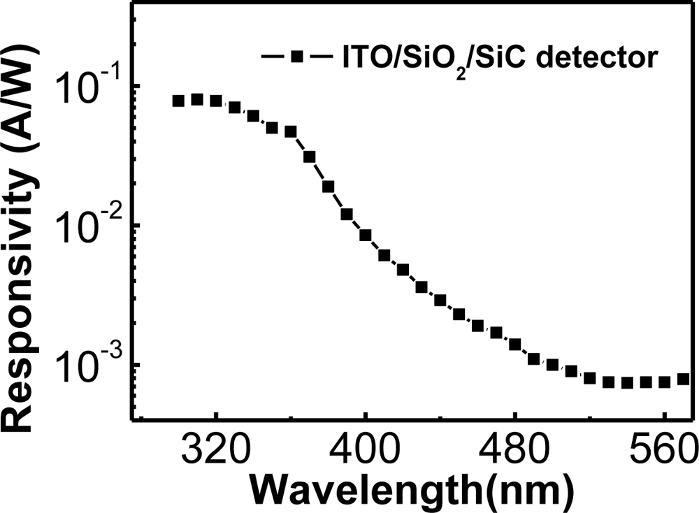
3.2. SiC MIS UV Photodetectors
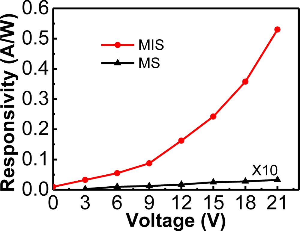
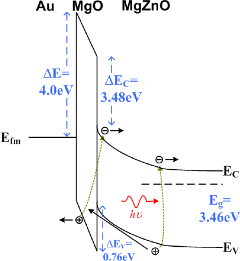
3.3. Zn-Based MIS UV Photodetectors
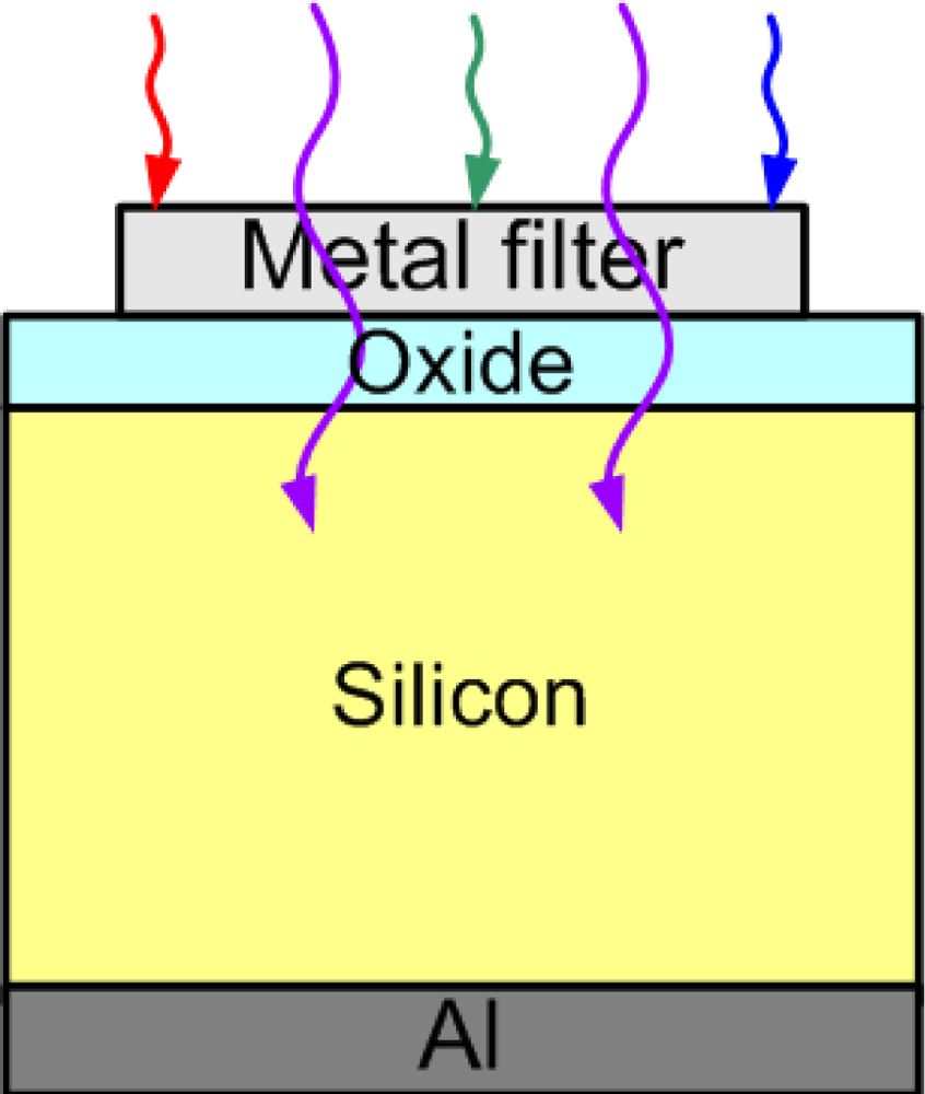
3.4. Metal-Filter Si MIS UV Photodetectors
4. MIS Visible-to-Near-IR Photodetectors
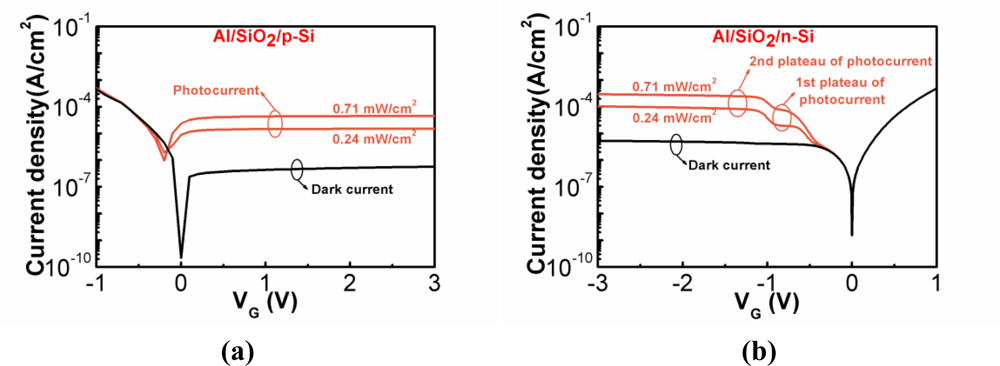
4.1. Si-Based MIS Visible-to-Near-IR Photodetectors
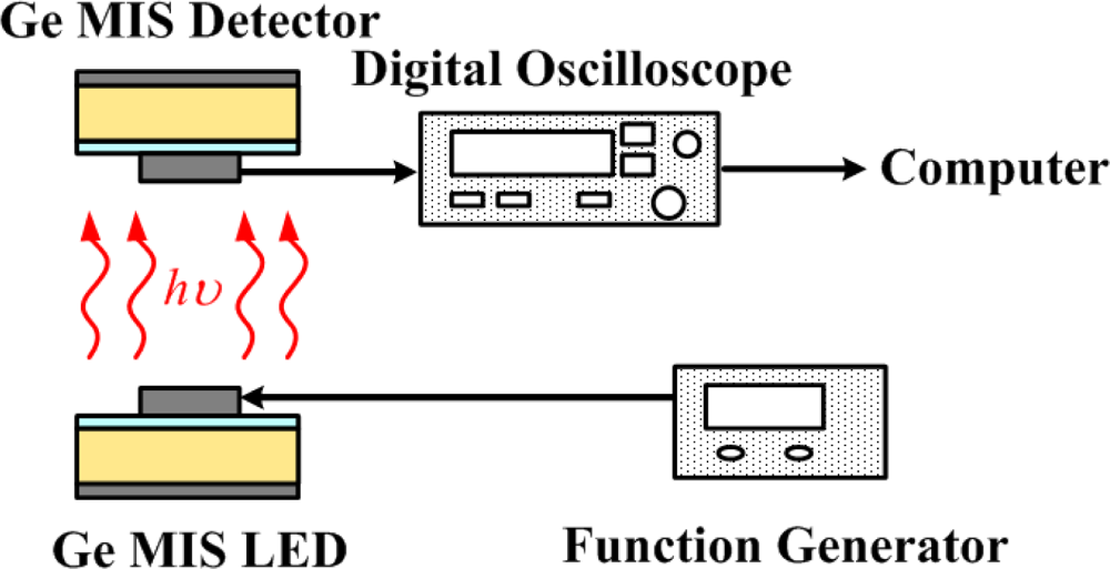
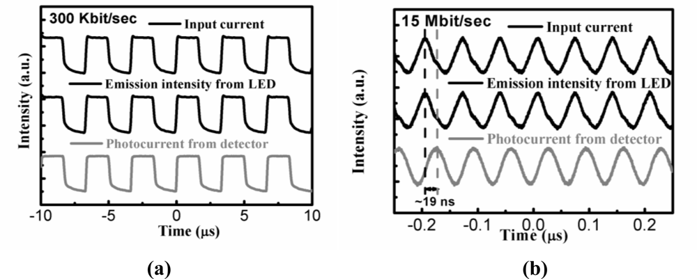
4.2. Bulk Ge MIS Visible-to-Near-IR Photodetectors
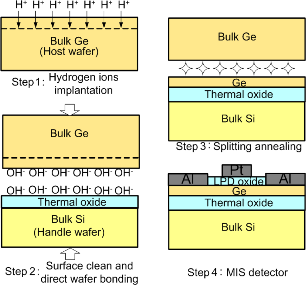
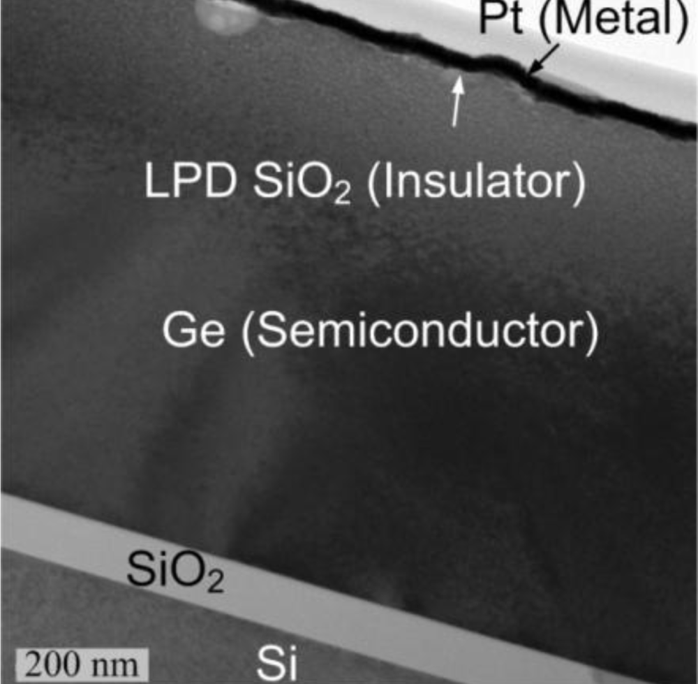
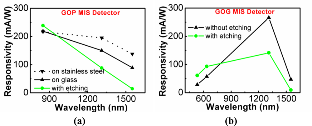
4.3. Thin-Film Ge MIS Visible-to-Near-IR Photodetectors
5. MIS IR Photodetectors
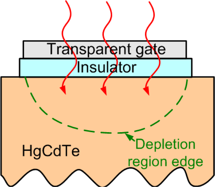
5.1. HgCdTe MIS IR Photodetectors
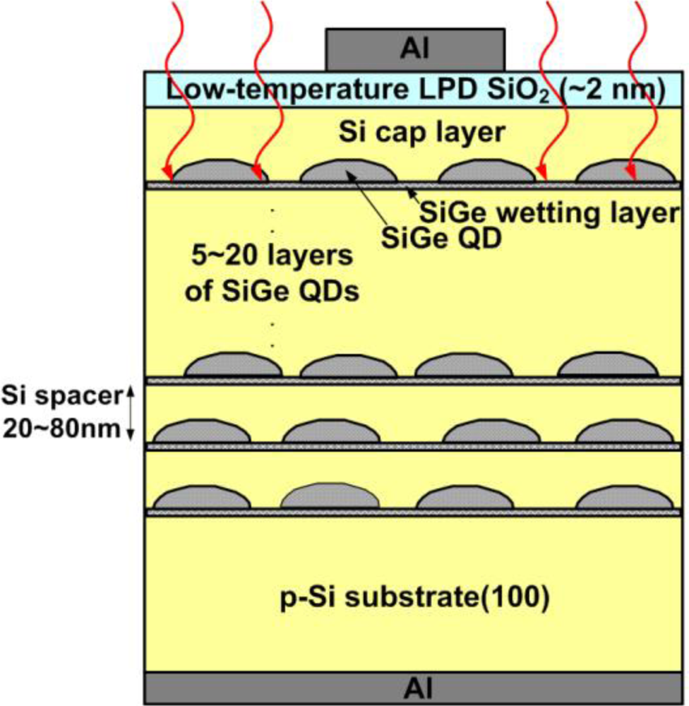
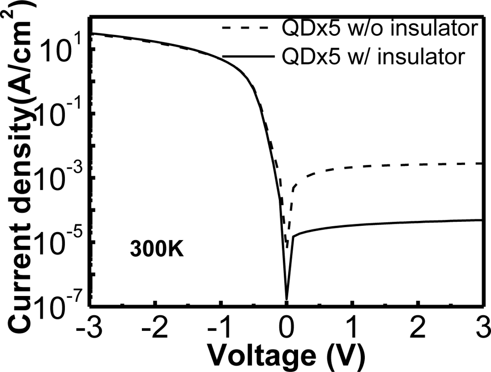
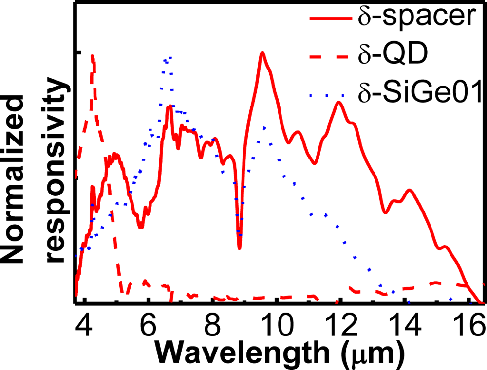
5.2. MIS SiGe/Si Quantum Dot (Well) IR Photodetectors
6. Conclusions
References
- Monroy, E; Omnès, F; Calle, F. Wide-Bandgap Semiconductor Ultraviolet Photodetectors. Semicond. Sci. Technol 2003, 18, R33–R51. [Google Scholar]
- Park, JS; Lin, TL; Jones, EW; Castillo, HMD; Gunapala, SD. Long-Wavelength Stacked SiGe/Si Heterojunction Internal Photoemission Infrared Detectors Using Multiple SiGe/Si Layers. Appl. Phys. Lett 1994, 64, 2370–2372. [Google Scholar]
- Rogalski, A. Quantum Well Photoconductors in Infrared Detector Technology. J. Appl. Phys 2003, 93, 4355–4391. [Google Scholar]
- Kasper, E; Oehme, M. High Speed Germanium Detectors on Si. Phys. Stat. Sol. C 2008, 5, 3144–3149. [Google Scholar]
- Brennan, KF; Haralson, J; Parks, JW; Salem, A. Review of Reliability Issues of Metal-Semiconductor-Metal and Avalanche Photodiode Photonic Detectors. Microelectron. Reliab 1999, 39, 1873–1883. [Google Scholar]
- Lee, HC; Su, YK; Lin, JC; Cheng, YC; Wu, SL; Jhou, YD. AlInGaN Metal-Insulator-Semiconductor Photodetectors at UV-C 280 nm. Electrochem. Solid. St 2009, 12, H357–H360. [Google Scholar]
- Lo, SH; Buchanan, DA; Taur, Y; Wang, W. Quantum-Mechanical Modeling of Electron Tunneling Current from the Inversion Layer of Ultra-Thin-Oxide MOSFET’s. IEEE. Electron. Device. Lett 1997, 18, 209–211. [Google Scholar]
- Lee, WC; Hu, C. Modeling CMOS Tunneling Currents Through Ultrathin Gate Oxide Due to Conduction and Valence Band Electron and Hole Tunneling. IEEE. Trans. Electron. Devices 2001, 48, 1366–1373. [Google Scholar]
- Liu, CW; Liu, WT; Lee, MH; Kuo, WS; Hsu, BC. A Novel Photodetector Using MOS Tunneling Structures. IEEE. Electron. Device. Lett 2000, 21, 307–309. [Google Scholar]
- Lin, CH; Hsu, BC; Lee, MH; Liu, CW. A Comprehensive Study of Inversion Current in MOS Tunneling Diodes. IEEE. Trans. Electron. Devices 2001, 48, 2125–2130. [Google Scholar]
- Sze, SM; Ng, KK. Physics of Semiconductor Devices, 3rd ed; Wiley: Hoboken, NJ, USA, 2007; p. 682. [Google Scholar]
- Monroy, E; Calle, F; Pau, JL; Muñoz, E; Omnès, F; Beaumont, B; Gibart, P. Application and Performance of GaN Based UV Detectors. Phys. Stat. Sol. A 2001, 185, 91–97. [Google Scholar]
- Sze, SM; Ng, KK. Physics of Semiconductor Devices, 3rd ed; Wiley: Hoboken, NJ, USA, 2007; p. 678. [Google Scholar]
- Liu, CY; Chen, BY; Tseng, TY. Deep Depletion Phenomenon of SrTiO3 Gate Dielectric Capacitor. J. Appl. Phys 2004, 95, 5602–5607. [Google Scholar]
- Liu, J; Michel, J; Giziewicz, W; Pan, D; Wada, K; Cannon, DD; Jongthammanurak, S; Danielson, DT; Kimerling, LC. High-Performance, Tensile-Strained Ge p-i-n Photodetectors on a Si Platform. Appl Phys Lett 2005, 87, 103501:1–103501:3. [Google Scholar]
- Monroy, E; Calle, F; Pau, JL; Muñoz, E; Omnès, F. Low-Noise Metal-Insulator-Semiconductor UV Photodiodes Based on GaN. Electron. Lett 2000, 36, 2096–2098. [Google Scholar]
- Basak, D; Amin, G; Mallik, B; Paul, GK; Sen, SK. Photoconductive UV Detectors on Sol-Gel-Synthesized ZnO Films. J. Cryst. Growth 2003, 256, 73–77. [Google Scholar]
- Muñoz, E; Monroy, E; Pau, JL; Calle, F; Omnès, F; Gibart, P, III. Nitrides and UV Detection. J. Phys. Condens. Matter 2001, 13, 7115–7137. [Google Scholar]
- Chiou, YZ; Su, YK; Chang, SJ; Gong, J; Chang, CS; Liu, SH. The Properties of Photo Chemical-Vapor Deposition SiO2 and its Application in GaN Metal-Insulator Semiconductor Ultraviolet Photodetectors. J. Electron. Mater 2002, 32, 395–399. [Google Scholar]
- Lin, CH; Yu, CY; Peng, CY; Ho, WS; Liu, CW. Broadband SiGe/Si Quantum Dot Infrared Photodetectors. J Appl Phys 2007, 101, 033117:1–033117:4. [Google Scholar]
- Hwang, JD; Yang, GH; Yang, YY; Yao, PC. Nitride-Based UV Metal-Insulator-Semiconductor Photodetector with Liquid-Phase-Deposition Oxide. Jpn. J. Appl. Phys 2005, 44, 7913–7915. [Google Scholar]
- Walker, D; Kumar, V; Mi, K; Sandvik, P; Kung, P; Zhang, XH; Razeghi, M. Solar-Blind AlGaN Photodiodes with Very Low Cutoff Wavelength. Appl. Phys. Lett 2000, 76, 403–405. [Google Scholar]
- Chang, PC; Chen, CH; Chang, SJ; Su, YK; Yu, CL; Huang, BR; Chen, PC. High UV/visible Rejection Contrast AlGaN/GaN MIS Photodetectors. Thin Solid Films 2006, 498, 133–136. [Google Scholar]
- Walker, D; Saxler, A; Kung, P; Zhang, X; Hamilton, M; Diaz, J; Razeghi, M. Visible Blind GaN p-i-n Photodiodes. Appl. Phys. Lett 1998, 72, 3303–3305. [Google Scholar]
- Zhang, Y; Shen, SC; Kim, HJ; Choi, S; Ryou, JH; Dupuis, RD; Narayan, B. Low-Noise GaN Ultraviolet p-i-n Photodiodes on GaN Substrates. Appl Phys Lett 2009, 94, 221109:1–221109:3. [Google Scholar]
- Carrano, JC; Grudowski, PA; Eiting, CJ; Dupuis, RD; Campbell, JC. Very Low Dark Current Metal-Semiconductor-Metal Ultraviolet Photodetectors Fabricated on Single-Crystal GaN Epitaxial Layers. Appl. Phys. Lett 1997, 70, 1992–1994. [Google Scholar]
- Wang, CK; Chang, SJ; Su, YK; Chiou, YZ; Chen, SC; Chang, CS; Lin, TK; Liu, HL; Tang, JJ. GaN MSM UV Photodetectors with Titanium Tungsten Transparent Electrodes. IEEE. Trans. Electron. Devices 2006, 53, 38–42. [Google Scholar]
- Yang, W; Nohova, T; Krishnankutty, S; Torreano, R; McPherson, S; Marsh, H. Back-Illuminated GaN/AlGaN Heterojunction Photodiodes with High Quantum Efficiency and Low Noise. Appl. Phys. Lett 1998, 73, 1086–1088. [Google Scholar]
- Ozbay, E; Biyikli, N; Kimukin, I; Kartaloglu, T; Tut, T; Aytür, O. High-Performance Solar-Blind Photodetectors Based on AlxGa1-xN Heterostructures. IEEE. J. Sel. Top. Quantum Electron 2004, 10, 742–751. [Google Scholar]
- Razeghi, M; Rogalski, A. Semiconductor Ultraviolet Detectors. J. Appl. Phys 1996, 79, 7433–7473. [Google Scholar]
- Liu, CH; Chang, CS; Chang, SJ; Su, YK; Chiou, YZ; Liu, SH; Huang, BR. The Characteristics of Photo-CVD SiO2 and Its Application on SiC MIS UV Photodetectors. Mater. Sci. Eng. B 2003, 100, 142–146. [Google Scholar]
- Chen, X; Zhu, H; Cai, J; Wu, Z. High-Performance 4H-SiC-Based Ultraviolet p-i-n Photodetector. J Appl Phys 2007, 102, 024505:1–024505:4. [Google Scholar]
- Morkoc, H; Strite, S; Gao, GB; Lin, ME; Sverdlov, B; Burns, M. Large-Band-Gap SiC, III–V Nitride, and II–VI ZnSe-Based Semiconductor Device Technologies. J. Appl. Phys 1994, 76, 1363–1398. [Google Scholar]
- Lin, TK; Chang, SJ; Chiou, YZ; Wang, CK; Chang, SP; Lam, KT; Sun, YS; Huang, BR. Homoepitaxial ZnSe MIS Photodetectors with SiO2 and BST Insulator Layers. Solid. State. Electron 2006, 50, 750–753. [Google Scholar]
- Young, SJ; Ji, LW; Chang, SJ; Liang, SH; Lam, KT; Fang, TH; Chen, KJ; Du, XL; Xue, QK. ZnO-Based MIS Photodetectors. Sens. Actuat. A. Phys 2008, 141, 225–229. [Google Scholar]
- Tsukazaki, A; Ohtomo, A; Onuma, T; Ohtani, M; Makino, T; Sumiya, M; Ohtani, K; Chichibu, SF; Fuke, S; Segawa, Y; Ohno, H; Koinuma, H; Kawasaki, M. Repeated Temperature Modulation Epitaxy for p-Type Doping and Light-Emitting Diode Based on ZnO. Nature Mater 2005, 4, 42–46. [Google Scholar]
- Zhu, H; Shan, CX; Wang, LK; Zheng, J; Zhang, JY; Yao, B; Shen, DZ. Metal-Oxide-Semiconductor-Structured MgZnO Ultraviolet Photodetector with High Internal Gain. J. Phys. Chem. C 2010, 114, 7169–7172. [Google Scholar]
- Yang, W; Vispute, RD; Choopun, S; Sharma, RP; Venkatesan, T; Shen, H. Ultraviolet Photoconductive Detector Based on Epitaxial Mg0.34Zn0.66O Thin Films. Appl. Phys. Lett 2001, 78, 2787–2789. [Google Scholar]
- Ju, ZG; Shan, CX; Jiang, DY; Zhang, JY; Yao, B; Zhao, DX; Shen, DZ; Fan, XW. MgxZn1-xO-Based Photodetectors Covering the Whole Solar-Blind Spectrum Range. Appl Phys Lett 2008, 93, 173505:1–173505:3. [Google Scholar]
- Ho, WS; Lin, CH; Cheng, TH; Hsu, WW; Chen, YY; Kuo, PS; Liu, CW. Narrow-Band Metal-Oxide-Semiconductor Photodetector. Appl Phys Lett 2009, 94, 061114:1–061114:3. [Google Scholar]
- Hansen, TE. Silicon UV-Photodiodes Using Natural Inversion Layers. Phys. Scr 1978, 18, 471–475. [Google Scholar]
- Colace, L; Assanto, G; Fulgoni, D; Nash, L. Near-Infrared p-i-n Ge-on-Si Photodiodes for Silicon Integrated Receivers. J. Lightwave. Technol 2008, 26, 2954–2959. [Google Scholar]
- Sher, A; Tsuo, YH; Moriarty, JA; Miller, WE; Crouch, RK. Si and GaAs Photocapacitive MIS Infrared Detectors. J. Appl. Phys 1980, 51, 2137–2148. [Google Scholar]
- Malik, A; Grimalsky, V. Conception of the Optical Sensors Based on Transient Processed in MIS Structures. Sens. Actuat. A. Phys 2004, 110, 310–317. [Google Scholar]
- Malik, A; Grimalsky, V; Jacome, AT; Durini, D. Theoretical Modeling and Experimental Investigation of MIS Radiation Sensor with Giant Internal Signal Amplification. Sens. Actuat. A. Phys 2004, 114, 319–326. [Google Scholar]
- Thaniyavarn, S; Gustafson, TK. Metal/Tunnel-Barrier/Semiconductor/Tunnel-Barrier/Metal Fast Photodetector. Appl. Phys. Lett 1982, 40, 255–257. [Google Scholar]
- Fernandes, M; Vygranenko, Y; Schwarz, R; Vieira, M. ITO/SiOx/Si Optical Sensor with Internal Gain. Sens. Actuat. A. Phys 2001, 92, 152–155. [Google Scholar]
- Hsu, BC; Chang, ST; Shie, CR; Lai, CC; Chen, PS; Liu, CW. High Efficient 820 nm MOS Ge Quantum Dot Photodetectors for Short-Reach Integrated Optical Receivers with 1,300 and 1,550 nm Sensitivity. IEDM Tech Dig 2002, 91–94. [Google Scholar]
- Cheng, JY; Lu, HT; Hwu, JG. Metal-Oxide-Semiconductor Tunneling Photodiodes with Enhanced Deep Depletion at Edge by High-k Material. Appl Phys Lett 2010, 96, 233506:1–233506:3. [Google Scholar]
- Hsu, BC; Liu, CW; Liu, WT; Lin, CH. A PMOS Tunneling Photodetector. IEEE. Trans. Electron. Devices 2001, 48, 1747–1749. [Google Scholar]
- Hashimoto, H; Yamada, R; Hirokane, T; Arima, K; Uchikoshi, J; Morita, M. Photodetective Characteristics of Metal-Oxide-Semiconductor Tunneling Structure with Aluminum Grid Gate. Jpn. J. Appl. Phys 2007, 46, 2467–2470. [Google Scholar]
- Seto, M; Rochefort, C; Jager, SD; Hendriks, RFM; ’t Hooft, GW; Mark, MBVD. Low-Leakage-Current Metal-Insulator-Semiconductor-Insulator-Metal Photodetector on Silicon with a SiO2 Barrier-Enhancement Layer. Appl. Phys. Lett 1999, 75, 1976–1978. [Google Scholar]
- Hsu, BC; Chang, ST; Chen, TC; Kuo, PS; Chen, PS; Pei, Z; Liu, CW. A High Efficient 820 nm MOS Ge Quantum Dot Photodetector. IEEE. Electron. Device. Lett 2003, 24, 318–320. [Google Scholar]
- Binari, SC; Miller, WE; Sher, A; Tsuo, YH. Ge Photocapacitive MIS Infrared Detectors. J. Appl. Phys 1979, 50, 7883–7886. [Google Scholar]
- Cheng, TH; Liao, MH; Yeh, L; Lee, TL; Liang, MS. Digital Communication Using Ge Metal-Insulator-Semiconductor Light-Emitting Diodes and Photodetectors. J Appl Phys 2008, 103, 016103:1–016103:3. [Google Scholar]
- Kuo, PS; Fu, YC; Chang, CC; Lee, CH; Liu, CW. Dark Current Reduction of Ge MOS Photodetectors by High Work Function Electrodes. Electron. Lett 2007, 43, 1113–1114. [Google Scholar]
- Morse, M; Dosunmu, O; Sarid, G; Chetrit, Y. Performance of Ge-on-Si p-i-n Photodetectors for Standard Receiver Modules. IEEE. Photon. Technol. Lett 2006, 18, 2442–2444. [Google Scholar]
- Zang, H; Lee, SJ; Loh, WY; Wang, J; Yu, MB; Lo, GQ; Kwong, DL; Cho, BJ. Application of Dopant Segregation to Metal-Germanium-Metal Photodetectors and Its Dark Current Suppression Mechanism. Appl Phys Lett 2008, 92, 051110:1–051110:3. [Google Scholar]
- Yu, CY; Lee, CY; Lin, CH; Liu, CW. Low-Temperature Fabrication and Characterization of Ge-on-Insulator Structures. Appl Phys Lett 2006, 89, 101913:1–101913:3. [Google Scholar]
- Nishimura, T; Kita, K; Toriumi, A. Evidence for Strong Fermi-Level Pinning Due to Metal-Induced Gap States at Metal/Germanium Interface. Appl Phys Lett 2007, 91, 123123:1–123123:3. [Google Scholar]
- Lieten, RR; Degroote, S; Kuijk, M; Borghs, G. Ohmic Contact Formation on n-Type Ge. Appl Phys Lett 2008, 92, 022106:1–022106:3. [Google Scholar]
- Lin, CH; Chiang, YT; Hsu, CC; Lee, CH; Huang, CF; Lai, CH; Cheng, TH; Liu, CW. Ge-on-Glass Detectors. Appl Phys Lett 2007, 91, 041105:1–041105:3. [Google Scholar]
- Ho, WS; Dai, YH; Deng, Y; Lin, CH; Chen, YY; Lee, CH; Liu, CW. Flexible Ge-on-Polyimide Detectors. Appl Phys Lett 2009, 94, 261107:1–261107:3. [Google Scholar]
- Heyns, M; Meuris, M; Caymax, M. Ge and III/V as Enabling Materials for Future CMOS Technologies. ECS Trans 2006, 3, 511–518. [Google Scholar]
- Rogalski, A. Infrared Detectors: Status and Trends. Prog. Quantum. Electron 2003, 27, 59–210. [Google Scholar]
- Deng, SY; Lee, JYM; Lai, JT; Chih, YD; Sun, TP; Hong, HM. Front-Illuminated Long Wavelength Multiple Quantum-Well Infrared Photodetectors with Backside Gratings. J. Appl. Phys 1995, 78, 6822–6825. [Google Scholar]
- Finkman, E; Maimon, S; Immer, V; Bahir, G; Schacham, SE; Fossard, F; Julien, FH; Brault, J; Gendry, M. Polarized Front-Illumination Response in Intraband Quantum Dot Infrared Photodetectors at 77 K. Phys Rev B 2001, 63, 045323:1–045323:7. [Google Scholar]
- Rogalski, A. HgCdTe Infrared Detector Material: History, Status and Outlook. Rep. Prog. Phys 2005, 68, 2267–2336. [Google Scholar]
- Singh, R; Gupta, AK; Chhabra, KC. Surface Passivation of Mercury-Cadmium-Telluride Infrared Detectors. Def. Sci. J 1991, 41, 205–239. [Google Scholar]
- Kinch, MA. MIS Devices in HgCdTe. In Properties of Narrow Gap Cadmium-Based Compounds (EMIS Datareviews Series No 10); Capper, P, Ed.; INSPEC, IEE: London, UK, 1994; pp. 359–363. [Google Scholar]
- Lee, TS; Choi, KK; Jeoung, YT; Kim, HK; Kim, JM; Kim, YH; Chang, JM; Song, WS; Kim, SU; Park, MJ; Lee, SD. Surface Passivation of HgCdTe by CdZnTe and Its Characteristics. J. Electron. Mater 1997, 26, 552–555. [Google Scholar]
- Jung, YC; An, SY; Suh, SH; Choi, DK; Kim, JS. Ammonium Sulfide Treatment of HgCdTe Substrate and Its Effects on Electrical Properties of ZnS/HgCdTe Heterostructure. Thin Solid Films 2005, 483, 407–410. [Google Scholar]
- Damnjanoviè, V; Ponomarenko, VP; Elazar, JM. Photo-Electric Characteristics of HgCdTe Tunnel MIS Photo-Detectors. Semicond Sci Technol 2009, 24, 025003:1–025003:6. [Google Scholar]
- Karunasiri, RPG; Park, JS; Wang, KL. Si1-xGex/Si Multiple Quantum Well Infrared Detector. Appl. Phys. Lett 1991, 59, 2588–2590. [Google Scholar]
- Kruck, P; Helm, M; Fromherz, T; Bauer, G; Nützel, JF; Abstreiter, G. Medium-Wavelength, Normal-Incidence, p-Type Si/SiGe Quantum Well Infrared Photodetector with Background Limited Performance up to 85 K. Appl. Phys. Lett 1996, 69, 3372–3374. [Google Scholar]
- Tong, S; Liu, F; Khitun, A; Wang, KL; Liu, JL. Tunable Normal Incidence Ge Quantum Dot Midinfrared Detectors. J. Appl. Phys 2004, 96, 773–776. [Google Scholar]
- Hsu, BC; Lin, CH; Kuo, PS; Chang, ST; Chen, PS; Liu, CW; Lu, JH; Kuan, CH. Novel MIS Ge-Si Quantum-Dot Infrared Photodetectors. IEEE. Electron. Device. Lett 2004, 25, 544–546. [Google Scholar]
- Liu, JL; Wu, WG; Balandin, A; Jin, GL; Wang, KL. Intersubband Absorption in Boron-Doped Multiple Ge Quantum Dots. Appl. Phys. Lett 1992, 74, 185–187. [Google Scholar]
- Kuo, PS; Lin, CH; Peng, CY; Fu, YC; Liu, CW. Transport Mechanism of SiGe Dot MOS Tunneling Diodes. IEEE. Electron. Device. Lett 2007, 28, 596–598. [Google Scholar]
- Lin, CH; Yu, CY; Kuo, PS; Chang, CC; Guo, TH; Liu, CW. Doped MOS Ge/Si Quantum Dot/Well Infrared Photodetector. Thin Solid Films 2006, 508, 389–392. [Google Scholar]
- Lin, CH; Yu, CY; Chang, CC; Lee, CH; Yang, YJ; Ho, WS; Chen, YY; Liao, MH; Cho, CT; Peng, CY; Liu, CW. SiGe/Si Quantum-Dot Infrared Photodetectors with Doping. IEEE Trans. Nanotech 2008, 7, 558–564. [Google Scholar]
- Liao, MH; Lee, CH; Hung, TA; Liu, CW. The Intermixing and Strain Effects on Electroluminescence of SiGe Dots. J Appl Phys 2007, 102, 053520:1–053520:5. [Google Scholar]
- Lin, CH; Liu, CW. Metal-Oxide-Semiconductor SiGe/Si Quantum Dot Infrared Photodetectors with Delta Doping in Different Positions. Thin Solid Films 2010, 518, S237–S240. [Google Scholar]


| Device | Jrev (Jinv) (A/cm2) | Responsivity (mA/W) | Detectivity (cmHz0.5W−1) | Rejection ratio | Ref. |
|---|---|---|---|---|---|
| MIS ITO/photo-SiO2/GaN | 5 × 10⁻⁷ @1 V | 110@338 nm@3 V | 2 × 10⁸@16 V | ∼200@3 V | [19] |
| MIS Al/LPD-SiO2/GaN | 7 × 10⁻⁷ @1 V | 112@366 nm@10 V | [21] | ||
| p-i-n GaN | 6 × 10⁻⁸@1 V | 150@363 nm@0 V | 106@0 V | [24] | |
| p-i-n GaN | 4 × 10⁻¹¹@10 V | 140@360 nm@20 V | 1.7 × 10¹⁴@20 V | 8×10³@20 V | [25] |
| MSM GaN | 4.5 × 10⁻⁶@10 V | 300@350 nm@6 V | ∼200@6 V | [26] | |
| MSM GaN | 10−6@1 V | 192@361 nm@3 V | 6.4 × 10⁹@3 V | ∼103@3 V | [27] |
| MIS AlGaN/GaN | ∼10−6 @1 V | 144@350 nm@5 V | 3,000@5 V | [23] | |
| p-i-n AlGaN/GaN | 6 × 10⁻¹⁰ @1 V | 200@355 nm@0 V | 104@0 V | [28] | |
| p-i-n AlGaN/GaN | 3 × 10⁻¹¹ @6 V | 65@267 nm@0 V | 4.9 × 10¹⁴@0 V | ∼104@0 V | [29] |
| MSM AlGaN/GaN | ∼10−6 @6 V | 2@264 nm@0 V | 8.9 × 10¹⁰@0 V | 2 × 10⁴@0 V | [29] |
| MSM AlGaN/GaN | ∼10−3 @1 V | 2@350 nm@5 V | 200@5 V | [23] | |
© 2010 by the authors; licensee MDPI, Basel, Switzerland. This article is an open access article distributed under the terms and conditions of the Creative Commons Attribution license (http://creativecommons.org/licenses/by/3.0/).
Share and Cite
Lin, C.-H.; Liu, C.W. Metal-Insulator-Semiconductor Photodetectors. Sensors 2010, 10, 8797-8826. https://doi.org/10.3390/s101008797
Lin C-H, Liu CW. Metal-Insulator-Semiconductor Photodetectors. Sensors. 2010; 10(10):8797-8826. https://doi.org/10.3390/s101008797
Chicago/Turabian StyleLin, Chu-Hsuan, and Chee Wee Liu. 2010. "Metal-Insulator-Semiconductor Photodetectors" Sensors 10, no. 10: 8797-8826. https://doi.org/10.3390/s101008797
APA StyleLin, C.-H., & Liu, C. W. (2010). Metal-Insulator-Semiconductor Photodetectors. Sensors, 10(10), 8797-8826. https://doi.org/10.3390/s101008797