
Spin State Switching in Heptauthrene Nanostructure by Electric Field: Computational Study


Abstract
:1. Introduction
2. Methods
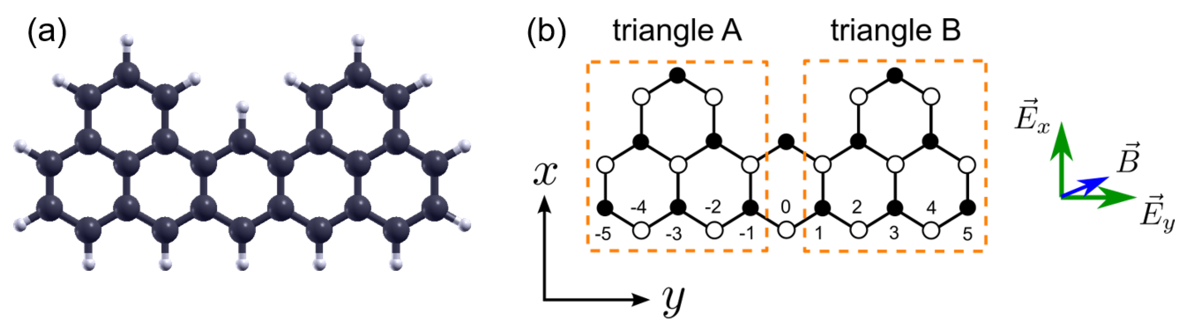
3. Results
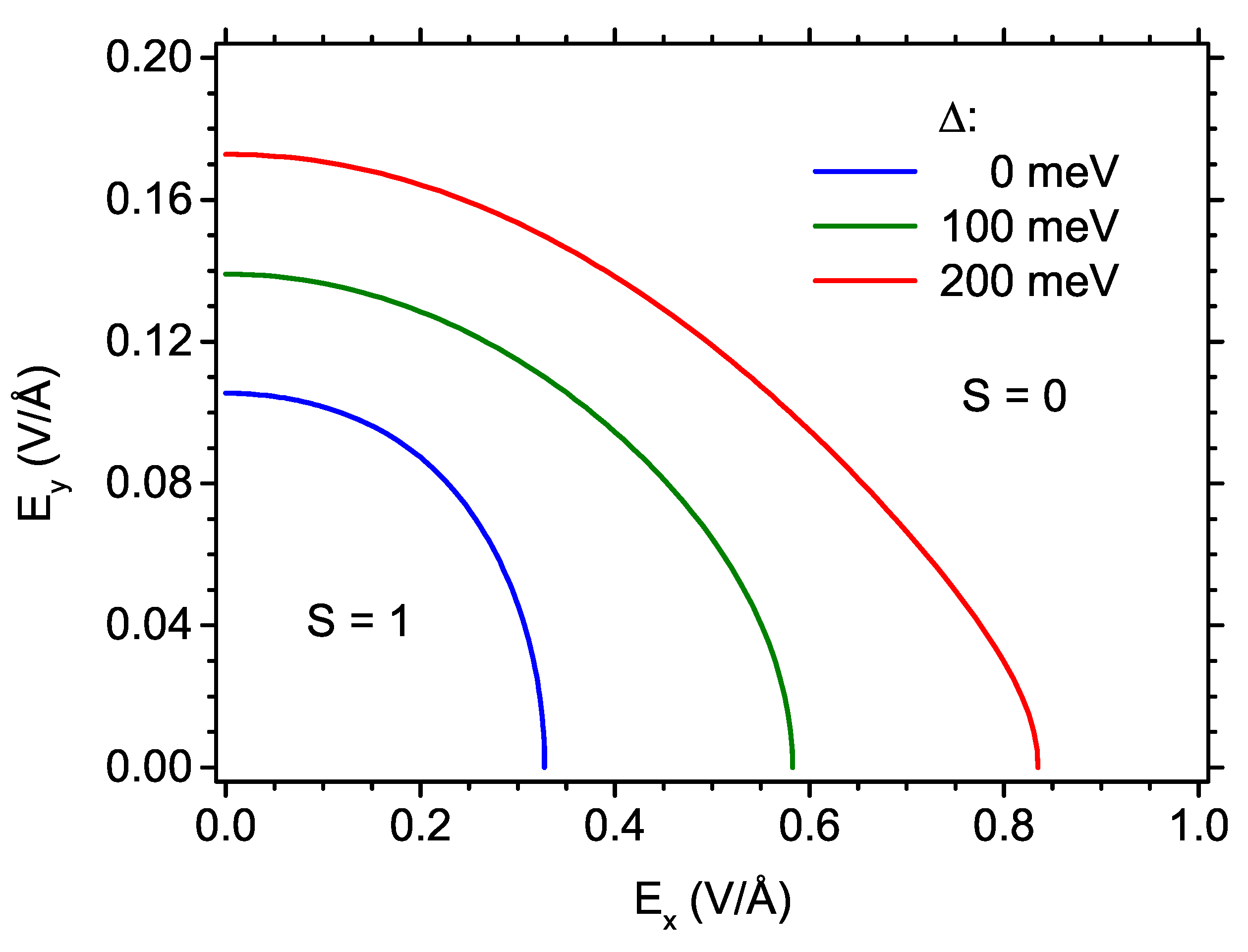
3.1. Magnetic Phase Diagrams
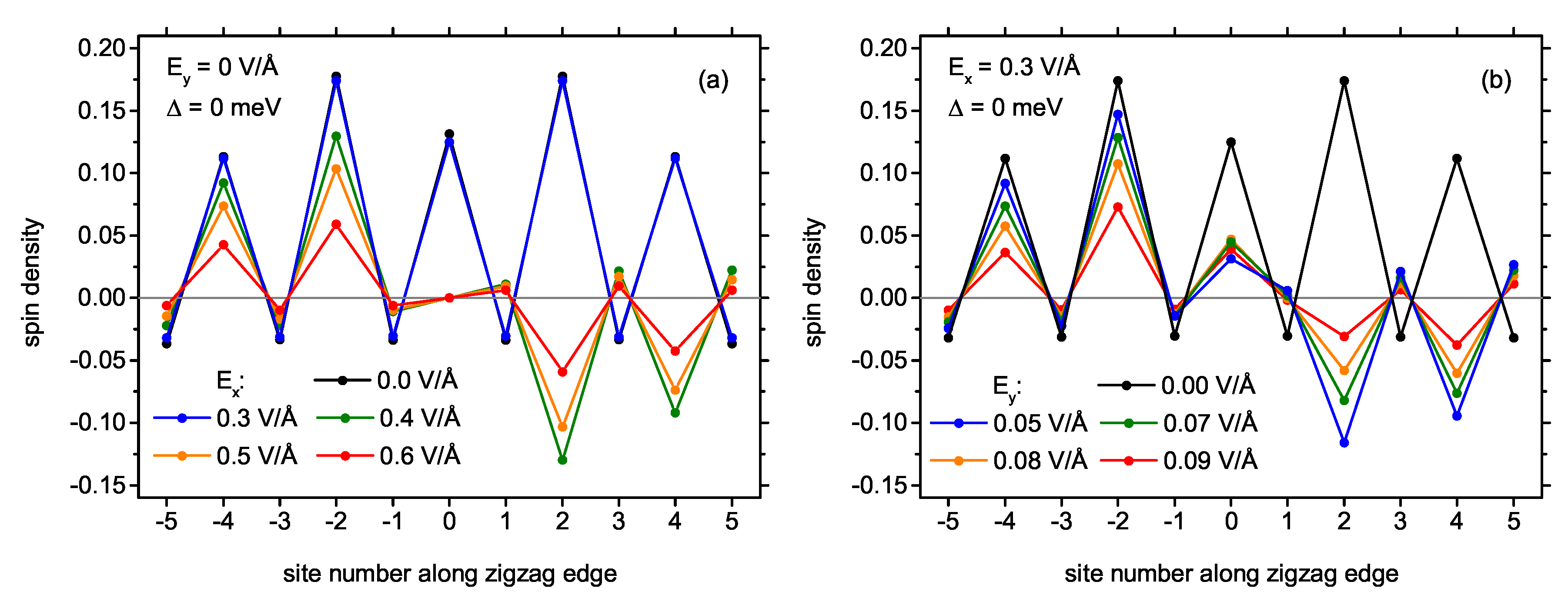
3.2. Spin Distribution and Energy States
4. Discussion
5. Conclusions
Funding
Institutional Review Board Statement
Informed Consent Statement
Data Availability Statement
Conflicts of Interest
Abbreviations
| AFM | antiferromagnetic |
| NM | non-magnetic |
References
- Ramesh, R.; Manipatruni, S. Electric Field Control of Magnetism. Proc. R. Soc. A Math. Phys. Eng. Sci. 2021, 477, 20200942. [Google Scholar] [CrossRef]
- Sahoo, S.; Kontos, T.; Furer, J.; Hoffmann, C.; Gräber, M.; Cottet, A.; Schönenberger, C. Electric Field Control of Spin Transport. Nat. Phys. 2005, 1, 99–102. [Google Scholar] [CrossRef] [Green Version]
- Matsukura, F.; Tokura, Y.; Ohno, H. Control of Magnetism by Electric Fields. Nat. Nanotechnol. 2015, 10, 209–220. [Google Scholar] [CrossRef] [PubMed]
- Yan, H.; Feng, Z.; Qin, P.; Zhou, X.; Guo, H.; Wang, X.; Chen, H.; Zhang, X.; Wu, H.; Jiang, C.; et al. Electric-Field-Controlled Antiferromagnetic Spintronic Devices. Adv. Mater. 2020, 32, 1905603. [Google Scholar] [CrossRef]
- Bogani, L.; Wernsdorfer, W. Molecular Spintronics Using Single-Molecule Magnets. Nat. Mater. 2008, 7, 179–186. [Google Scholar] [CrossRef]
- Camarero, J.; Coronado, E. Molecular vs. Inorganic Spintronics: The Role of Molecular Materials and Single Molecules. J. Mater. Chem. 2009, 19, 1678–1684. [Google Scholar] [CrossRef]
- Sanvito, S. Molecular Spintronics. Chem. Soc. Rev. 2011, 40, 3336–3355. [Google Scholar] [CrossRef] [PubMed]
- Han, W.; Kawakami, R.K.; Gmitra, M.; Fabian, J. Graphene Spintronics. Nat. Nanotechnol. 2014, 9, 794–807. [Google Scholar] [CrossRef]
- Bullard, Z.; Girão, E.C.; Owens, J.R.; Shelton, W.A.; Meunier, V. Improved All-Carbon Spintronic Device Design. Sci. Rep. 2015, 5, 7634. [Google Scholar] [CrossRef] [PubMed] [Green Version]
- Avsar, A.; Ochoa, H.; Guinea, F.; Özyilmaz, B.; van Wees, B.J.; Vera-Marun, I.J. Colloquium: Spintronics in Graphene and Other Two-Dimensional Materials. Rev. Mod. Phys. 2020, 92, 021003. [Google Scholar] [CrossRef]
- Wu, J.; Pisula, W.; Müllen, K. Graphenes as Potential Material for Electronics. Chem. Rev. 2007, 107, 718–747. [Google Scholar] [CrossRef]
- Narita, A.; Wang, X.Y.; Feng, X.; Müllen, K. New Advances in Nanographene Chemistry. Chem. Soc. Rev. 2015, 44, 6616–6643. [Google Scholar] [CrossRef] [Green Version]
- Clar, E. Polycyclic Hydrocarbons: Volume 1; Springer: Berlin/Heidelberg, Germany, 1964. [Google Scholar] [CrossRef]
- Clar, E. Polycyclic Hydrocarbons: Volume 2; Springer: Berlin/Heidelberg, Germany, 1964. [Google Scholar] [CrossRef]
- Sun, Q.; Zhang, R.; Qiu, J.; Liu, R.; Xu, W. On-Surface Synthesis of Carbon Nanostructures. Adv. Mater. 2018, 30, 1705630. [Google Scholar] [CrossRef]
- Yan, L.; Liljeroth, P. Engineered Electronic States in Atomically Precise Artificial Lattices and Graphene Nanoribbons. Adv. Phys. X 2019, 4, 1651672. [Google Scholar] [CrossRef] [Green Version]
- Talirz, L.; Ruffieux, P.; Fasel, R. On-Surface Synthesis of Atomically Precise Graphene Nanoribbons. Adv. Mater. 2016, 28, 6222–6231. [Google Scholar] [CrossRef]
- Kolmer, M.; Steiner, A.K.; Izydorczyk, I.; Ko, W.; Engelund, M.; Szymonski, M.; Li, A.P.; Amsharov, K. Rational Synthesis of Atomically Precise Graphene Nanoribbons Directly on Metal Oxide Surfaces. Science 2020, 369, 571–575. [Google Scholar] [CrossRef] [PubMed]
- Song, S.; Su, J.; Telychko, M.; Li, J.; Li, G.; Li, Y.; Su, C.; Wu, J.; Lu, J. On-Surface Synthesis of Graphene Nanostructures with π-Magnetism. Chem. Soc. Rev. 2021, 50, 3238–3262. [Google Scholar] [CrossRef] [PubMed]
- Su, J.; Telychko, M.; Hu, P.; Macam, G.; Mutombo, P.; Zhang, H.; Bao, Y.; Cheng, F.; Huang, Z.Q.; Qiu, Z.; et al. Atomically Precise Bottom-up Synthesis of π-Extended [5]Triangulene. Sci. Adv. 2019, 5, eaav7717. [Google Scholar] [CrossRef] [PubMed] [Green Version]
- Mishra, S.; Beyer, D.; Eimre, K.; Liu, J.; Berger, R.; Gröning, O.; Pignedoli, C.A.; Müllen, K.; Fasel, R.; Feng, X.; et al. Synthesis and Characterization of π-Extended Triangulene. J. Am. Chem. Soc. 2019, 141, 10621–10625. [Google Scholar] [CrossRef]
- Mishra, S.; Beyer, D.; Eimre, K.; Kezilebieke, S.; Berger, R.; Gröning, O.; Pignedoli, C.A.; Müllen, K.; Liljeroth, P.; Ruffieux, P.; et al. Topological Frustration Induces Unconventional Magnetism in a Nanographene. Nat. Nanotechnol. 2020, 15, 22–28. [Google Scholar] [CrossRef]
- Mishra, S.; Xu, K.; Eimre, K.; Komber, H.; Ma, J.; Pignedoli, C.A.; Fasel, R.; Feng, X.; Ruffieux, P. Synthesis and Characterization of [7]Triangulene. Nanoscale 2021, 13, 1624–1628. [Google Scholar] [CrossRef] [PubMed]
- Mishra, S.; Beyer, D.; Eimre, K.; Ortiz, R.; Fernández-Rossier, J.; Berger, R.; Gröning, O.; Pignedoli, C.A.; Fasel, R.; Feng, X.; et al. Collective All-Carbon Magnetism in Triangulene Dimers. Angew. Chem. Int. Ed. 2020, 59, 12041–12047. [Google Scholar] [CrossRef] [Green Version]
- Mishra, S.; Yao, X.; Chen, Q.; Eimre, K.; Gröning, O.; Ortiz, R.; Di Giovannantonio, M.; Sancho-García, J.C.; Fernández-Rossier, J.; Pignedoli, C.A.; et al. Large Magnetic Exchange Coupling in Rhombus-Shaped Nanographenes with Zigzag Periphery. Nat. Chem. 2021, 13, 581–586. [Google Scholar] [CrossRef]
- Zhang, H.; Lu, J.; Zhang, Y.; Gao, L.; Zhao, X.J.; Tan, Y.Z.; Cai, J. Engineering the Magnetism of Nanographene via Co-Depositing Hetero Precursors. Res. Sq. 2021. [Google Scholar] [CrossRef]
- Hieulle, J.; Castro, S.; Friedrich, N.; Vegliante, A.; Lara, F.R.; Sanz, S.; Rey, D.; Corso, M.; Frederiksen, T.; Pascual, J.I.; et al. On-Surface Synthesis and Collective Spin Excitations of a Triangulene-Based Nanostar. Angew. Chem. Int. Ed. 2021, 60, 25224–25229. [Google Scholar] [CrossRef]
- Su, J.; Fan, W.; Mutombo, P.; Peng, X.; Song, S.; Ondráček, M.; Golub, P.; Brabec, J.; Veis, L.; Telychko, M.; et al. On-Surface Synthesis and Characterization of [7]Triangulene Quantum Ring. Nano Lett. 2021, 21, 861–867. [Google Scholar] [CrossRef] [PubMed]
- Mishra, S.; Catarina, G.; Wu, F.; Ortiz, R.; Jacob, D.; Eimre, K.; Ma, J.; Pignedoli, C.A.; Feng, X.; Ruffieux, P.; et al. Observation of Fractional Edge Excitations in Nanographene Spin Chains. Nature 2021, 598, 287–292. [Google Scholar] [CrossRef] [PubMed]
- Wang, X.Y.; Yao, X.; Narita, A.; Müllen, K. Heteroatom-Doped Nanographenes with Structural Precision. Accounts Chem. Res. 2019, 52, 2491–2505. [Google Scholar] [CrossRef] [Green Version]
- Fernández-Rossier, J.; Palacios, J.J. Magnetism in Graphene Nanoislands. Phys. Rev. Lett. 2007, 99, 177204. [Google Scholar] [CrossRef] [Green Version]
- Ezawa, M. Metallic Graphene Nanodisks: Electronic and Magnetic Properties. Phys. Rev. B 2007, 76, 245415. [Google Scholar] [CrossRef] [Green Version]
- Wang, W.L.; Meng, S.; Kaxiras, E. Graphene NanoFlakes with Large Spin. Nano Lett. 2008, 8, 241–245. [Google Scholar] [CrossRef] [PubMed]
- Yazyev, O.V. Emergence of Magnetism in Graphene Materials and Nanostructures. Rep. Prog. Phys. 2010, 73, 056501. [Google Scholar] [CrossRef]
- Lieb, E.H. Two Theorems on the Hubbard Model. Phys. Rev. Lett. 1989, 62, 1201–1204. [Google Scholar] [CrossRef]
- Ortiz, R.; Boto, R.A.; García-Martínez, N.; Sancho-García, J.C.; Melle-Franco, M.; Fernández-Rossier, J. Exchange Rules for Diradical π-Conjugated Hydrocarbons. Nano Lett. 2019, 19, 5991–5997. [Google Scholar] [CrossRef] [Green Version]
- Zheng, Y.; Li, C.; Xu, C.; Beyer, D.; Yue, X.; Zhao, Y.; Wang, G.; Guan, D.; Li, Y.; Zheng, H.; et al. Designer Spin Order in Diradical Nanographenes. Nat. Commun. 2020, 11, 6076. [Google Scholar] [CrossRef]
- Zhong, Q.; Ihle, A.; Ahles, S.; Wegner, H.A.; Schirmeisen, A.; Ebeling, D. Constructing Covalent Organic Nanoarchitectures Molecule by Molecule via Scanning Probe Manipulation. Nat. Chem. 2021, 13, 1133–1139. [Google Scholar] [CrossRef] [PubMed]
- Potasz, P.; Güçlü, A.D.; Hawrylak, P. Zero-Energy States in Triangular and Trapezoidal Graphene Structures. Phys. Rev. B 2010, 81, 033403. [Google Scholar] [CrossRef] [Green Version]
- Rycerz, A. Strain-Induced Transitions to Quantum Chaos and Effective Time-Reversal Symmetry Breaking in Triangular Graphene Nanoflakes. Phys. Rev. B 2013, 87, 195431. [Google Scholar] [CrossRef] [Green Version]
- Jin, H.; Li, J.; Wang, T.; Yu, Y. Photoinduced Pure Spin-Current in Triangulene-Based Nano-Devices. Carbon 2018, 137, 1–5. [Google Scholar] [CrossRef]
- Fujita, M.; Wakabayashi, K.; Nakada, K.; Kusakabe, K. Peculiar Localized State at Zigzag Graphite Edge. J. Phys. Soc. Jpn. 1996, 65, 1920–1923. [Google Scholar] [CrossRef] [Green Version]
- Klusek, Z.; Waqar, Z.; Denisov, E.A.; Kompaniets, T.N.; Makarenko, I.V.; Titkov, A.N.; Bhatti, A.S. Observations of Local Electron States on the Edges of the Circular Pits on Hydrogen-Etched Graphite Surface by Scanning Tunneling Spectroscopy. Appl. Surf. Sci. 2000, 161, 508–514. [Google Scholar] [CrossRef]
- Güçlü, A.D.; Potasz, P.; Voznyy, O.; Korkusinski, M.; Hawrylak, P. Magnetism and Correlations in Fractionally Filled Degenerate Shells of Graphene Quantum Dots. Phys. Rev. Lett. 2009, 103, 246805. [Google Scholar] [CrossRef] [Green Version]
- Potasz, P.; Güçlü, A.D.; Wójs, A.; Hawrylak, P. Electronic Properties of Gated Triangular Graphene Quantum Dots: Magnetism, Correlations, and Geometrical Effects. Phys. Rev. B 2012, 85, 075431. [Google Scholar] [CrossRef] [Green Version]
- Güçlü, A.D.; Potasz, P.; Korkusinski, M.; Hawrylak, P. Magnetic Properties of Gated Graphene Nanostructures. In Graphene Quantum Dots; Güçlü, A.D., Potasz, P., Korkusinski, M., Hawrylak, P., Eds.; NanoScience and Technology; Springer: Berlin/Heidelberg, Germany, 2014; pp. 111–144. [Google Scholar] [CrossRef]
- Güçlü, A.D.; Potasz, P.; Hawrylak, P. Sublattice Engineering and Voltage Control of Magnetism in Triangular Single and Bi-Layer Graphene Quantum Dots. Phys. Status Solidi (RRL) Rapid Res. Lett. 2016, 10, 58–67. [Google Scholar] [CrossRef] [Green Version]
- Dong, Q.; Jiang, F.; Lian, S.; Liu, C. Electric-Field Control of the Degenerate Shell in a Triangular Graphene Quantum Dot. J. Magn. Magn. Mater. 2019, 476, 225–228. [Google Scholar] [CrossRef]
- Dong, Q. Electrical Spin Switch in a Two-Electron Triangular Graphene Quantum Dot. Phys. E Low-Dimens. Syst. Nanostruct. 2020, 116, 113779. [Google Scholar] [CrossRef]
- Dong, Q.; Yin, X.; Liu, C. The Effect of Size and Applied Electric Field on the Spin Switch in a Two-Electron Graphene Quantum Dot and Graphene Qubit. Phys. E Low-Dimens. Syst. Nanostruct. 2021, 127, 114555. [Google Scholar] [CrossRef]
- Ma, W.L.; Li, S.S. Electric-Field-Induced Spin Depolarization in Graphene Quantum Dots. Phys. Rev. B 2012, 86, 045449. [Google Scholar] [CrossRef]
- Dong, Q.R.; Li, Y.; Jia, C.; Wang, F.L.; Zhang, Y.T.; Liu, C.X. Electrically-Induced Polarization Selection Rules of a Graphene Quantum Dot. Solid State Commun. 2018, 273, 55–59. [Google Scholar] [CrossRef] [Green Version]
- Szałowski, K. Graphene Nanoflakes in External Electric and Magnetic In-Plane Fields. J. Magn. Magn. Mater. 2015, 382, 318–327. [Google Scholar] [CrossRef] [Green Version]
- Ortiz, R.; García-Martínez, N.A.; Lado, J.L.; Fernández-Rossier, J. Electrical Spin Manipulation in Graphene Nanostructures. Phys. Rev. B 2018, 97, 195425. [Google Scholar] [CrossRef] [Green Version]
- Sheng, W.; Luo, K.; Zhou, A. Electric Field Induced Spin Polarization in Graphene Nanodots. Phys. Rev. B 2014, 90, 085406. [Google Scholar] [CrossRef]
- Zhou, A.; Sheng, W.; Xu, S.J. Electric Field Driven Magnetic Phase Transition in Graphene Nanoflakes. Appl. Phys. Lett. 2013, 103, 133103. [Google Scholar] [CrossRef] [Green Version]
- Zhou, A.; Sheng, W. Magnetic Phase Diagram of Graphene Nanorings in an Electric Field. J. Phys. Condens. Matter 2015, 27, 406002. [Google Scholar] [CrossRef]
- Güçlü, A.D.; Potasz, P.; Hawrylak, P. Electric-Field Controlled Spin in Bilayer Triangular Graphene Quantum Dots. Phys. Rev. B 2011, 84, 035425. [Google Scholar] [CrossRef] [Green Version]
- Sharifian, M.; Hoseini, S.S.; Faizabadi, E. Ground State Magnetic Properties in AA-Stacking Bilayer Graphene Quantum Dots Using Lieb’s Theorem. J. Magn. Magn. Mater. 2019, 477, 427–433. [Google Scholar] [CrossRef]
- Sharifian, M.; Faizabadi, E. The Influence of AA and AB Stacking on the Ground State Magnetic Properties of Triangular Bilayer Graphene Quantum Dots. J. Magn. Magn. Mater. 2021, 529, 167822. [Google Scholar] [CrossRef]
- Szałowski, K. Ferrimagnetic and Antiferromagnetic Phase in Bilayer Graphene Nanoflake Controlled with External Electric Fields. Carbon 2017, 118, 78–85. [Google Scholar] [CrossRef] [Green Version]
- Sivasubramani, S.; Debroy, S.; Acharyya, S.G.; Acharyya, A. Tunable Intrinsic Magnetic Phase Transition in Pristine Single-Layer Graphene Nanoribbons. Nanotechnology 2018, 29, 455701. [Google Scholar] [CrossRef]
- Apinyan, V.; Kopeć, T.K. Antiferromagnetic Ordering and Excitonic Pairing in AA-Stacked Bilayer Graphene. Phys. Rev. B 2021, 104, 075426. [Google Scholar] [CrossRef]
- Basak, T.; Shukla, A. Optical Signatures of Electric-Field-Driven Magnetic Phase Transitions in Graphene Quantum Dots. Phys. Rev. B 2016, 93, 235432. [Google Scholar] [CrossRef] [Green Version]
- Qi, J.; Hu, K.; Li, X. Electric Control of the Edge Magnetization in Zigzag Stanene Nanoribbons from First Principles. Phys. Rev. Appl. 2018, 10, 034048. [Google Scholar] [CrossRef] [Green Version]
- Ildarabadi, F.; Farghadan, R. Fully Spin-Valley-Polarized Current Induced by Electric Field in Zigzag Stanene and Germanene Nanoribbons. Phys. Chem. Chem. Phys. 2021, 23, 6084–6090. [Google Scholar] [CrossRef] [PubMed]
- Li, J.; Sanz, S.; Corso, M.; Choi, D.J.; Peña, D.; Frederiksen, T.; Pascual, J.I. Single Spin Localization and Manipulation in Graphene Open-Shell Nanostructures. Nat. Commun. 2019, 10, 200. [Google Scholar] [CrossRef] [PubMed] [Green Version]
- Li, J.; Sanz, S.; Castro-Esteban, J.; Vilas-Varela, M.; Friedrich, N.; Frederiksen, T.; Peña, D.; Pascual, J.I. Uncovering the Triplet Ground State of Triangular Graphene Nanoflakes Engineered with Atomic Precision on a Metal Surface. Phys. Rev. Lett. 2020, 124, 177201. [Google Scholar] [CrossRef] [PubMed]
- Su, X.; Li, C.; Du, Q.; Tao, K.; Wang, S.; Yu, P. Atomically Precise Synthesis and Characterization of Heptauthrene with Triplet Ground State. Nano Lett. 2020, 20, 6859–6864. [Google Scholar] [CrossRef] [PubMed]
- Kokalj, A. XCrySDen—a New Program for Displaying Crystalline Structures and Electron Densities. J. Mol. Graph. Model. 1999, 17, 176–179. [Google Scholar] [CrossRef]
- Feldner, H.; Meng, Z.Y.; Honecker, A.; Cabra, D.; Wessel, S.; Assaad, F.F. Magnetism of Finite Graphene Samples: Mean-Field Theory Compared with Exact Diagonalization and Quantum Monte Carlo Simulations. Phys. Rev. B 2010, 81, 115416. [Google Scholar] [CrossRef] [Green Version]
- Hancock, Y.; Uppstu, A.; Saloriutta, K.; Harju, A.; Puska, M.J. Generalized Tight-Binding Transport Model for Graphene Nanoribbon-Based Systems. Phys. Rev. B 2010, 81, 245402. [Google Scholar] [CrossRef] [Green Version]
- Ijäs, M.; Ervasti, M.; Uppstu, A.; Liljeroth, P.; van der Lit, J.; Swart, I.; Harju, A. Electronic States in Finite Graphene Nanoribbons: Effect of Charging and Defects. Phys. Rev. B 2013, 88, 075429. [Google Scholar] [CrossRef] [Green Version]
- Magda, G.Z.; Jin, X.; Hagymási, I.; Vancsó, P.; Osváth, Z.; Nemes-Incze, P.; Hwang, C.; Biró, L.P.; Tapasztó, L. Room-Temperature Magnetic Order on Zigzag Edges of Narrow Graphene Nanoribbons. Nature 2014, 514, 608–611. [Google Scholar] [CrossRef] [PubMed] [Green Version]
- Ribeiro, R.M.; Pereira, V.M.; Peres, N.M.R.; Briddon, P.R.; Neto, A.H.C. Strained Graphene: Tight-Binding and Density Functional Calculations. New J. Phys. 2009, 11, 115002. [Google Scholar] [CrossRef] [Green Version]
- Pereira, V.M.; Castro Neto, A.H.; Peres, N.M.R. Tight-Binding Approach to Uniaxial Strain in Graphene. Phys. Rev. B 2009, 80, 045401. [Google Scholar] [CrossRef] [Green Version]
- Yang, H.X.; Hallal, A.; Terrade, D.; Waintal, X.; Roche, S.; Chshiev, M. Proximity Effects Induced in Graphene by Magnetic Insulators: First-Principles Calculations on Spin Filtering and Exchange-Splitting Gaps. Phys. Rev. Lett. 2013, 110, 046603. [Google Scholar] [CrossRef] [Green Version]
- Hallal, A.; Ibrahim, F.; Yang, H.; Roche, S.; Chshiev, M. Tailoring Magnetic Insulator Proximity Effects in Graphene: First-Principles Calculations. 2D Mater. 2017, 4, 025074. [Google Scholar] [CrossRef]
- Dyrdał, A.; Barnaś, J. Anomalous, Spin, and Valley Hall Effects in Graphene Deposited on Ferromagnetic Substrates. 2D Mater. 2017, 4, 034003. [Google Scholar] [CrossRef] [Green Version]
- Žutić, I.; Matos-Abiague, A.; Scharf, B.; Dery, H.; Belashchenko, K. Proximitized Materials. Mater. Today 2019, 22, 85–107. [Google Scholar] [CrossRef]
- Bora, M.; Deb, P. Magnetic Proximity Effect in Two-Dimensional van Der Waals Heterostructure. J. Phys. Mater. 2021, 4, 034014. [Google Scholar] [CrossRef]
- Cabria, I.; Amovilli, C.; López, M.J.; March, N.H.; Alonso, J.A. Electrostrictive Deformations in Small Carbon Clusters, Hydrocarbon Molecules, and Carbon Nanotubes. Phys. Rev. A 2006, 74, 063201. [Google Scholar] [CrossRef]
- Guo, W.; Guo, Y. Giant Axial Electrostrictive Deformation in Carbon Nanotubes. Phys. Rev. Lett. 2003, 91, 115501. [Google Scholar] [CrossRef] [PubMed]
- Stroscio, J.A.; Eigler, D.M. Atomic and Molecular Manipulation with the Scanning Tunneling Microscope. Science 1991, 254, 1319–1326. [Google Scholar] [CrossRef] [PubMed] [Green Version]
- Sierra, J.F.; Fabian, J.; Kawakami, R.K.; Roche, S.; Valenzuela, S.O. Van Der Waals Heterostructures for Spintronics and Opto-Spintronics. Nat. Nanotechnol. 2021, 16, 856–868. [Google Scholar] [CrossRef]
- Kunstmann, J.; Özdoğan, C.; Quandt, A.; Fehske, H. Stability of Edge States and Edge Magnetism in Graphene Nanoribbons. Phys. Rev. B 2011, 83, 045414. [Google Scholar] [CrossRef] [Green Version]
- Krompiewski, S. Limited Robustness of Edge Magnetism in Zigzag Graphene Nanoribbons with Electrodes. Nanotechnology 2014, 25, 465201. [Google Scholar] [CrossRef] [Green Version]
- Luo, M. Bistability of Zigzag Edge Magnetism in Graphene Nanoribbons Induced by Electric Field. J. Phys. D Appl. Phys. 2021, 54, 325003. [Google Scholar] [CrossRef]
- Modarresi, M.; Roknabadi, M.R.; Shahtahmasebi, N. Spin Polarization Tuning in the Graphene Quantum Dot by Using In-Plane External Electric Field. J. Magn. Magn. Mater. 2014, 350, 6–11. [Google Scholar] [CrossRef]
- Weymann, I.; Barnaś, J.; Krompiewski, S. Manifestation of the Shape and Edge Effects in Spin-Resolved Transport through Graphene Quantum Dots. Phys. Rev. B 2012, 85, 205306. [Google Scholar] [CrossRef] [Green Version]
- Weymann, I.; Krompiewski, S.; Barnaś, J. Spin-Dependent Transport Through Graphene Quantum Dots. J. Nanosci. Nanotechnol. 2012, 12, 7525–7528. [Google Scholar] [CrossRef]
- Weymann, I.; Barnaś, J.; Krompiewski, S. Transport through Graphenelike Flakes with Intrinsic Spin-Orbit Interactions. Phys. Rev. B 2015, 92, 045427. [Google Scholar] [CrossRef] [Green Version]
- Wang, D.; Zhang, Z.; Zhang, J.; Deng, X.; Fan, Z.; Tang, G. Electronic and Magnetic Properties of Zigzag-Edged Hexagonal Graphene Ring Nanojunctions. Carbon 2015, 94, 996–1002. [Google Scholar] [CrossRef]
- Fan, Z.Q.; Sun, W.Y.; Zhang, Z.H.; Deng, X.Q.; Tang, G.P.; Xie, H.Q. Symmetry-Dependent Spin Transport Properties of a Single Phenalenyl or Pyrene Molecular Device. Carbon 2017, 122, 687–693. [Google Scholar] [CrossRef]
- Gmitra, M.; Fabian, J. Graphene on Transition-Metal Dichalcogenides: A Platform for Proximity Spin-Orbit Physics and Optospintronics. Phys. Rev. B 2015, 92, 155403. [Google Scholar] [CrossRef] [Green Version]
- Krompiewski, S. Edge Magnetism of Finite Graphene-like Nanoribbons in the Presence of Intrinsic Spin–Orbit Interaction and Perpendicular Electric Field. Nanotechnology 2016, 27, 315201. [Google Scholar] [CrossRef]
- Krompiewski, S. Selected Graphenelike Zigzag Nanoribbons with Chemically Functionalized Edges: Implications for Electronic and Magnetic Properties. Phys. Rev. B 2019, 100, 125421. [Google Scholar] [CrossRef] [Green Version]
- Krompiewski, S. One Edge Magnetic Configurations in Graphene, Stanene and Phosphorene Zigzag Nanoribbons. J. Magn. Magn. Mater. 2021, 534, 168036. [Google Scholar] [CrossRef]
- Ortiz, R.; Fernández-Rossier, J. Probing Local Moments in Nanographenes with Electron Tunneling Spectroscopy. Prog. Surf. Sci. 2020, 95, 100595. [Google Scholar] [CrossRef]


Publisher’s Note: MDPI stays neutral with regard to jurisdictional claims in published maps and institutional affiliations. |
© 2021 by the author. Licensee MDPI, Basel, Switzerland. This article is an open access article distributed under the terms and conditions of the Creative Commons Attribution (CC BY) license (https://creativecommons.org/licenses/by/4.0/).
Share and Cite
Szałowski, K. Spin State Switching in Heptauthrene Nanostructure by Electric Field: Computational Study. Int. J. Mol. Sci. 2021, 22, 13364. https://doi.org/10.3390/ijms222413364
Szałowski K. Spin State Switching in Heptauthrene Nanostructure by Electric Field: Computational Study. International Journal of Molecular Sciences. 2021; 22(24):13364. https://doi.org/10.3390/ijms222413364
Chicago/Turabian StyleSzałowski, Karol. 2021. "Spin State Switching in Heptauthrene Nanostructure by Electric Field: Computational Study" International Journal of Molecular Sciences 22, no. 24: 13364. https://doi.org/10.3390/ijms222413364
APA StyleSzałowski, K. (2021). Spin State Switching in Heptauthrene Nanostructure by Electric Field: Computational Study. International Journal of Molecular Sciences, 22(24), 13364. https://doi.org/10.3390/ijms222413364