Abstract
Two-dimensional (2D) semiconductors are being considered as alternative channel materials as silicon-based field-effect transistors (FETs) have reached their scaling limits. Recently, air-stable 2D selenium nanosheet FETs with a gate length of 5 µm were experimentally produced. In this study, we used an ab initio quantum transport approach to simulate sub-5 nm gate-length double-gate monolayer (ML) selenene FETs. When considering negative-capacitance technology and underlap, we found that 3 nm gate-length p-type ML selenene FETs can meet the 2013 ITRS standards for high-performance applications along the armchair and zigzag directions in the 2028 horizon. Therefore, ML selenene has the potential to be a channel material that can scale Moore’s law down to a gate length of 3 nm.
1. Introduction
The short channel effect of silicon field-effect transistors (FETs) exceeds the physical limits of FETs, making them difficult to apply [1,2,3]. Therefore, the search for a new material to replace silicon is crucial. When successfully foliated, two-dimensional (2D) semiconductors have begun competing with graphene as a future channel material [4,5]. The newly created 2D Xenes (silicene, phosphorene, tellurene, and so on) have the potential to surpass the limitations in practical applications because of their uniform thickness, higher electrostatic gate control, simple elemental composition, and other properties [6,7]. The on/off-state current ratio of sub-10 nm gate length (Lg) monolayer and bilayer tellurene FETs with p-type characteristics is 108 and 106, respectively [8,9]. The p-type monolayer (ML) tellurene transistor meets the criterion for the International Technology Roadmap for Semiconductors (ITRS), with a gate length of 4 nm [9]. Thus, investigating 2D monoelemental semiconductors, which have good carrier mobility and air stability for use in logic circuits, is required [6,7,9,10,11,12,13,14,15,16].
Selenium, which is known for its essential role in biological systems, has received attention in the realm of physical sciences [17,18,19,20,21,22]. The thermal properties of 2D α-selenene were investigated by Liu et al., revealing its remarkable thermophysical characteristics. At a temperature of 300 K, 2D α-selenene exhibited an excellent thermal conductivity of 3.04 W/(m·K). The study by Liu et al. further emphasized the crucial role played by relaxation time in controlling the thermal transport behavior of 2D α-selenene [23]. Lin et al. conducted a detailed investigation into the thermoelectric properties of 2D ML square selenene, using a comprehensive approach to reveal a significant anisotropy in the thermal performance of the material. These findings provided valuable insights into the complex relationship between directionality and the thermal transport behavior of ML square selinene [22].
The photonic properties of 2D selenium nanosheets have also been investigated, revealing remarkable findings regarding the photoresponsivity and temporal characteristics of selenium nanosheet phototransistors. The photoresponsivity measurement has achieved an impressive value of 263 A/W, accompanied by the rapid rise and fall times of 0.1 s and 0.12 s, respectively [17]. These results indicate that ML square selenene is a potential material for thermoelectric and photonic devices in the future.
Back-gated FETs were fabricated by employing p-type selenium nanosheets with 5 μm Lg, using the physical vapor-deposition technique. The resulting FETs demonstrated a low on-state current (Ion) of approximately 20 A/m at Vdd = 3 V, which can be attributed to the presence of zigzag edges in the selenium nanosheets. Selenene, a 2D form of selenium, is fabricated in such a way that it is atomically thin [17]. Nevertheless, there is currently a knowledge gap in the existing literature about the fabrication and characterization of sub-5 nm Lg selenene FETs (sub-5 FETs).
This study presents a theoretical evaluation of the performances of sub-5 FETs using ab inito quantum transport simulations. The ITRS high-performance (HP) criteria were met by the Ion of the 3 nm Lg p-type selenene FETs (p-type 3 FETs) with underlap (UL) along the armchair direction (arm-direction) and the Ion of the 1 nm Lg p-type selenene FETs (p-type 1 FETs) with UL were approximately 17.55% and 1.90%, respectively, for the ITRS HP criteria along the armchair and zigzag directions (the arm-direction and the zig-direction). After considering the negative-capacitance (NC) effect and UL, the p-type 3 FETs met the ITRS HP criteria along both the arm-direction and the zig-direction. These results demonstrate that ML selenene is a potential channel material that is capable of extending Moore’s law by 3 nm.
2. Result and Discussion
2.1. Device Structure
The optimal lattice parameters of ML selenene are a = 3.76 Å, c = 6.52 Å, based on previous theoretical work [19,20]. Lattice structures of ML selenene from both top and side views are presented in Figure 1a. Figure 1b depicts the band structure of ML selenene using a double-zeta polarized (DZP) basis set in QuantumATK, showing an indirect band gap of 1.0 eV and exceeding the expected theoretical value of 0.73 eV (DFT/PBE) by a small amount, which is close to the theoretical value of 1.13 eV (DFT/HSE06) [24,25]. Figure 1c presents the n- and p-doped ML selenene, serving as channels and electrodes for the sub-5-FETs. A UL area was the uncovered part of the channel by the gate electrode, which was added between the source/drain electrode and gate. UL is an effective method to extend the effective channel length [26,27,28]. We executed the test for doping concentration to provide the best possible device performance (Figure S1). According to the test for doping concentration, we found that the off-state current of the 5 nm gate length n-type selenene FETs can not meet Ioff for ITRS HP along the armchair direction, except for doping concentration n = 5 × 1012 cm−2, as shown in Figure S1. Thus, the on-state current of the 5 nm gate length p-type selenene FETs is higher than that of n-type selenene FETs. The slope of transfer characteristics curves of the 5 nm gate length p-type selenene FETs is larger than that of n-type selenene FETs. Therefore, the p-type ML selenene FETs perform better than the n-type ones in the device. As a result, we exclusively investigated p-type ML selenene FETs in the arm- and zig-directions, and we adopted the doping concertation to 5 × 1013 cm−2 in the following calculations.
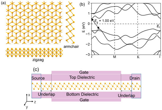
Figure 1.
(a) Lattice structure of ML selenene (top and side view). (b) Band structure of ML selenene. (c) Schematic view of the ML selenene FETs.
2.2. On-State Current
A critical figure of merit for the logic transistor is the Ion. Figure 2 depicts the transfer characteristic curve of the sub-5 FETs along the arm- and zig-directions. According to ITRS 2013, Vdd is the power supply voltage, chosen as Vdd = 0.64 V, Ioff = 0.1 μA/μm. We can obtain the off-state voltage (Vg,off) from transfer characteristics curves of the sub-5 nm gate lengths selenene FETs at the off-state current (Ioff). Thus, the on-state voltage and current (Vg,on and Ion) can be obtained. Figure 2 can determine Vg,on = Vg,off ±Vdd (“+” and “−” sign corresponds to n- and p-types) [29]. The power supply voltage is denoted by Vdd, according to ITRS 2013, Vdd = 0.64 V, Ioff = 0.1 μA/μm. The transfer current is calculated using the width normalization, and the width is 3.761 Å (6.515 Å) along the arm-(zig-) direction throughout the whole paper. All the p-type sub-5 FETs without UL cannot comply with the ITRS HP requirement along the arm- and zig-directions. After summarizing Ion in various Lg and UL lengths listed in Table 1 and Table 2, suitable UL lengths could significantly improve Ion for both the arm- and zig-directions in the ITRS HP application. The Ion of the p-type 3 FETs with LUL = 3 nm was 1010.32 μA/μm along the armchair directions, whereas the Ion (571.02 μA/μm) of the p-type 3 FETs with LUL = 2 nm was 63% of the ITRS for HP goal along the zig-directions, as shown in Figure 3.
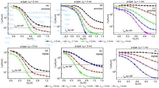
Figure 2.
Transfer characteristics of the p-type sub-5 FETs with LUL = 0, 1, 2, 3, and 4 nm (a–c) along the armchair and (d–f) zigzag direction. The bias is 0.64 V. Black dashed lines represent the ITRS HP requirements for the off-state current.

Table 1.
Benchmark of the ballistic performance of the p-type sub-5 FETs (along the armchair direction) against the ITRS 2013 requirements for HP transistors of the next decades.
Table 2.
Benchmark of the ballistic performance of the p-type sub-5 FETs (along the zigzag direction) against the ITRS 2013 requirements for HP transistors of the next decades.
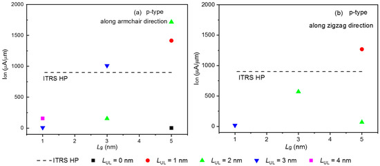
Figure 3.
On-state current as a function of the p-type sub-5 FETs with different gate lengths for HP applications along the (a) armchair and (b) zigzag direction.
Figure 4 presents spectrum characteristics of the 5 nm Lg p-type selenene FETs (p-type 5 FETs) with LUL = 1 nm in the HP application, allowing us to observe gate modulation along the arm-direction. Examples will be shown to demonstrate the spectrum current and position-resolved local density of states (LDOS) at on-, intermediate-, and off-states. The distance between the source’s Fermi level and the channel’s lowest valence band maximum is known as the hole activation energy (ΦB). As Vg rises from 0.08 to 0.72 V, the channel’s band edge tilts downwards, increasing from 0 to 0.34 eV. Consequently, the total current (Itotal) in the device comprises tunnel and thermal current (Itunnel and Itherm). Figure S2 depicts the 5 FETs with LUL = 1 nm in the zig-direction. The gate modulation mechanism of the p-type 5 FETs with LUL = 1 nm in the zig-direction is similar to that in the arm-direction. The related transmission eigenstates are the transport conditions in the on-, intermediate-, and off-state with E = 0.38 eV. Figure 4 and Figure S2 depict the transmission eigenstates of p-type 5 FETs with LUL = 1 nm at E = −0.38 eV in the on-, intermediate-, and off-state, respectively.
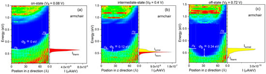
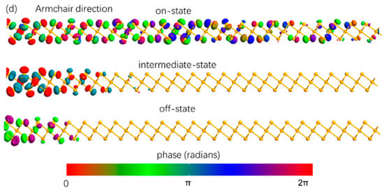
Figure 4.
(a–c) LDOS and spectrum current of the p-type 5 FETs with LUL = 1 nm at the on-, intermediate- and off-state for the HP applications along the armchair direction. μs(d) are the electrochemical potentials of the source (drain), respectively. ΦB is the activation energy height. (d) On-, intermediate-, and off-state transmission eigenstates of the p-type 5-FETs with LUL = 1 nm at E = −0.38 eV. The isovalue is 0.05 a.u.
2.3. Gate Controlling Ability
The subthreshold swing (SS = ∂Vg/∂(logIds)) is crucial in determining the ability of ML selenene FET to gate control [9,14]. We can obtain the SS from transfer characteristics curves of the sub-5 nm gate lengths selenene FETs in the subthreshold zone. A smaller SS offers higher gate control capability in the subthreshold zone. Figure 5 illustrates how the UL structure promotes SS growth as the Lg decreases in the p-type 5 FETs. Along the arm-direction, the SS of the p-type 5/3/1 FETs with UL structure is 100.39/117.19/178.68 mV/decade, respectively. The SS of the p-type sub-5 FETs with UL structure along the zig-direction is similar to that of the device in the arm-direction.
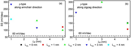
Figure 5.
SS versus Lg in the p-type sub-5 FETs with different underlap lengths (a) along the armchair direction (b) along the zigzag direction.
2.4. τ, PDP and EDP
The switching speed of ML selenene FETs is determined by the effective delay time (τ = CtVdd/Ion). Ct = Cg + Cf, Cg(f) is the gate (fringing) capacitance, and Cg = ∂Qch/∂Vg. According to ITRS 2013, Cg is equal to half of Cf. The QuantumATK 2019 software package was used with the DZP basis set to derive the total Mulliken charge (Qch) in the central region [24]. Furthermore, the Ct values of the p-type sub-5 FETs are smaller than the ITRS HP goal along the arm-direction. However, the Ct (0.2 fF/μm) of the p-type 3 FETs with LUL = 3 nm is smaller than the ITRS HP along the zig-direction, as shown in Figure S3. The Ct of p-type 3 FETs along the arm-direction is lower than that of the ones along the zig-direction for the same Lg. The response speed of the p-type 3 FETs in the arm-direction is faster than the device along the zig-direction, because of combining small Ct and large Ion to create a high-speed switch.
The switching energy of ML selenene FETs is measured using power dissipation (PDP = VddIonτ). Figure S4 shows that the PDP values of the p-type sub-5 FETs decrease with increasing Lg along both the arm- and zig-directions. Along the arm-direction, all PDPs of the p-type ML selenene FETs with UL can meet the ITRS HP criteria.
In Figure 6, we also include the energy–delay product (EDP) of p-type sub-5 FETs. EDP can be defined as EDP = PDP × τ, taking into account both response speed and energy dissipation. The minimum EDP value specified by ITRS requirements, as well as the EDP values for p-type sub-5 FETs and ML Teurene (Te) FETs reports, are plotted in red, pink, and blue lines, respectively. Except for the p-type 3 and 1 FETs with UL along a zig-direction, all of the p-type sub-5 FETs have EDP values that are lower than the EDP of ITRS HP criteria for the 2028 horizon (1.02 × 10⁻²⁸ J·s/μm). The p-type ML selenene FETs have the lowest EDP value at 1.5 × 10⁻²⁹ J·s/μm when Lg is set to 3 nm. It can be compared with those of ML MoS2 [30], InSe [31], Bi2O2Se [32], and Tellurene FETs [9]. The EDP of p-type ML selenene FETs is higher than that of ML InSe, Bi2O2Se, and tellurene FETs. It is roughly 17 times greater than the minimum EDP (9.02 × 10⁻³¹ J·s/μm) for ML tellurene FETs, but only slightly higher than the minimum EDP (1.34 × 10⁻³⁰ J·s/μm) for ML MoS2 FETs.
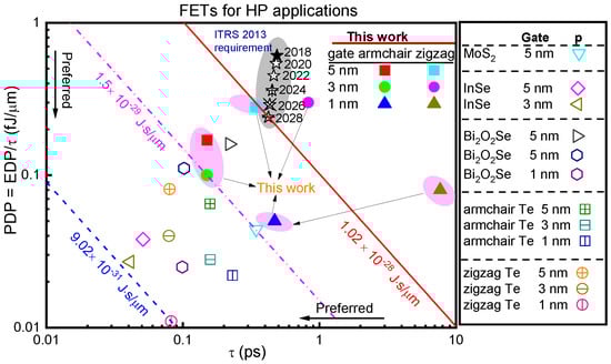
Figure 6.
PDP versus τ of ML MoS2 [30], InSe [31], Bi2O2Se [32], and Tellurene FETs (along the arm- and zig-direction) [9] for the HP applications, respectively. Solid lines are the minimum ITRS requirements for the energy–delay product EDP = τ × PDP. Dot and dash dot lines are the minimum EDP value of the p-type sub-5 FETs and ML tellurene FETs reports, respectively.
2.5. Discussion
Many 2D transistors are suitable for HP applications, such as ML MoS2 [30], ML InSe [31], ML and bilayer (BL) Bi2O2Se [32,33], ML and BL tellurene [8,9], and ML silicane [15], and so on. Several transport simulations of 2D semiconductors transistors based on the DFT + NEGF method are used to explore the potential channel candidates for post-silicon nanoelectronics. ML MoS2 and ML silicane can extend Moore’s law to 5 nm, respectively. ML InSe can extend Moore’s law to 3 nm. ML and BL Bi2O2Se can extend Moore’s law to 2 and 5 nm, respectively. ML and BL tellurene can extend Moore’s law to 4 and 9 nm, respectively.
The Ion is a critical figure of merit for the logic transistor, to figure out the key factor that affects Ion, the relationship between the effective mass (m*) and Ion of the suggested model at various 5 nm Lg 2D semiconductors FETs is displayed in Figure 7 [9,30,31,32]. When m* < 0.68 m0, Ion decreases with increasing m*, and Ion is at its lowest when m* ≈ 0.68 m0. For m* > 0.68 m0, Ion increases with increasing m*. Tiny m* results in a higher Ion and greater carrier velocities (v = eEτ/m*), which are determined by the e (charge), E (electric field), and τ, respectively. The current can be written as I = nev, where n is the carrier concentration. The density of states (DOS) of the transport channel is negligibly tiny. DOS is written as , where gs(v) is the spin (valley) degeneracies, is the reduced Plank constant, and is the transverse (transport) effective mass. Larger m* leads to slower velocity, but the DOS of the transport channel is enough; thus, Ion is high. According to Figure 7, the competition between m* and DOS results in a dominant factor affecting Ion. The anisotropy has been found in many 2D materials, such as ML BP [34,35], 2D BiAs [36], ML and BL tellurene [8,9], and ML selinene [19], and so on. The physical properties (elastic modulus, effective mass, deformation potential, and carrier mobility) of ML selenene are different between the arm- and zig-direction. Using the software package QuantumATK 2019, the effective mass (m*) of ML selenene was obtained from the band structure; the hole effective mass of ML selenene is 0.14 m0 and 0.43 m0 along the arm- and zig-direction, respectively. It is consistent with previous reports in the literature [19]. The hole effective mass of ML selenene along the arm-direction is lighter than that of the zig-direction, and the Ion (1717.80 μA/μm) of p-type 5 FETs along the arm-direction is larger than that (1269.00 μA/μm) of the device along the zig-direction, as shown in Table S1. The Ion of ML selenene are different between arm- and zig-direction with 3 nm and 1 nm gate length. Along the arm-direction, the m* (0.14 m0) of the hole for ML selenene is lighter than that (0.39 m0) of the ML tellurene, the Ion (1717.81 μA/μm) of ML selenene is larger than that (951 μA/μm) of ML tellurene. Along the zig-direction, the effective mass (0.43 m0) of ML selenene is larger than that (0.11 m0) of ML tellurene, so the Ion (1269 μA/μm) of ML selenene is smaller than that (2114 μA/μm) of ML tellurene.
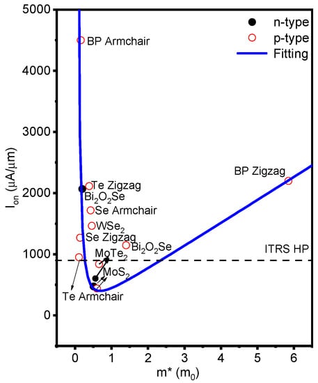
Figure 7.
The on-state current versus the effective mass of n- and p-type 5 FETs, and ML 2D channel materials for HP applications. All the data are calculated by ab initio quantum transport simulations. The solid curve line is a visual guide. The dashed line is the ITRS HP requirements of the 2013 edition.
We added a negative-capacitance (NC) gate stack to the ferroelectric materials to further enhance the performances of the p-type sub-5 FETs in Figure S5a [9,37]. We found that the Ion of the device increased, and the SS of p-type sub-5 FETs with the same Lg and UL decreased, but the Ion of the device increased. It is already known that the NC voltage is VNC = −3.822 × 10⁸ × tFEQ + 2.3529 × 10¹⁰ tFEQ3 of Hf0.5Zr0.5O2 ferroelectric material [38,39]. The electrical charge is represented by the symbol Q. The thickness of the ferroelectric layer is denoted by tFE, and for the ML selenene FETs, we incorporated a ferroelectric layer that was 50 nm thick.
Tables S2 and S3 compare the Ion and SS with those without NC for p-type sub-5 FETs with and without NC at LUL = 2 nm. Figure S5b compares the arm- and zig-direction transfer properties of p-type sub-5 FETs at Lg = 5 nm. Generally, the SS of p-type sub-5 FETs with NC is lower than those of p-type sub-5 FETs without NC. The minimum value of SS (81.26 mV/dec) is obtained by p-type 5 FETs with NC and LUL = 2 nm along the arm-direction. The Ion of p-type sub-5 nm FETs with NC is greater than those of p-type sub-5 FETs without NC. All Ion of p-type 5 FETs and 3 FETs with NC and UL satisfy the 2028 requirements (900 µA/µm) of ITRS HP application along arm- and zig-direction, respectively. The maximum value of Ion (3202.95 µA/µm) is obtained by p-type 5 FETs with NC and LUL = 2 nm along the arm-direction. In contrast, the maximum value of Ion is 3.55 times greater than the ITRS criteria for HP application.
3. Model and Approach
Using the software package QuantumATK Version P-2019.03, which combines the density functional theory (DFT) and the nonequilibrium Green’s function (NEGF), the transport characteristics of sub-5 FETs can be determined [24,26,40,41]. The following Landauer–Bűttiker formula is used to determine the drain current at a given bias (gate) voltage Vb(G) [41]:
where e and h are the elementary charges and the Planck constant, respectively, and the electrochemical potential and the Fermi–Dirac distribution function for the source (drain) are denoted by μS(D) and fS(D), respectively. The transmission coefficient is denoted by T(E, Vb, VG). FHI pseudopotential is used with the basis set of polarized double zeta. The exchange–correlation interaction is described using the generalized gradient approximation (GGA) as the Perdew–Burke–Ernzerhof (PBE) function [26,42,43,44]. The DFT method, which is based on GGA with single-electron approximation, is useful in characterizing a device’s electronic structure. This method is effective in modeling the electronic behavior of a device by doping the carriers with a strongly screened electron–electron interaction [45]. The k-point meshes in the Brillouin zone are set to Monkhorst–Pack 7 × 1 × 145 for the electrode and the central region. The temperature and real-space mesh cutoff are 300 K and 30 Ha, respectively. The boundary conditions for the x, y, and z axes are Neumann, Periodic, and Dirichlet, respectively. The z-axis is always the path of transport.
4. Conclusions
In the current work, the performance of the sub-5 FETs was first examined. With the proper UL structure, the Ion, τ, and PDP of the p-type 3 (5) FETs satisfy the ITRS HP criteria along the arm-(zig-)directions. After considering the NC effect and UL, the p-type 3 FETs can meet ITRS HP criteria along both arm- and zig-directions. Therefore, ML selenene has the potential to be used as a channel material for HP devices and extend Moore’s Law down to the 3 nm scale.
Supplementary Materials
The following supporting information can be downloaded at: https://www.mdpi.com/article/10.3390/molecules28145390/s1. Figure S1: Transfer characteristics of the n- and p-type 5 FETs with varying doping concentrations along arm- and zig-directions; Figure S2: LDOS and spectrum current of the p-type 5 FETs with LUL = 1 nm at the on-, intermediate- and off-state; Figures S3 and S4: the τ and PDP vs. Lg in the p-type sub-5 FETs with different UL along the arm- and zig-directions; Figure S5: A schematic presentation of the ML selenene FETs with the ferroelectric layers; Transfer characteristics of the p-type 5 FETs at LUL = 2 nm with and without NC dielectric; Tables S1–S3: Summary of Ion and SS values of the p-type sub-5 FETs for the HP application between with and without NC dielectric along the arm- and zig-direction.
Author Contributions
Q.L. is an expert in 2D materials and transistors. He was involved in performing the conceptualization, software, methodology, writing, and funding acquisition. X.T. is an expert in 2D materials and transistors. He was involved in performing the conceptualization, software, methodology, writing, and validation. Y.Y. is an expert in 2D materials and transistors. He was involved in performing the conceptualization, methodology, writing, and validation. X.X. is an expert in 2D materials and 2D materials transistors. He was involved in performing the software, formal analysis, writing, and validation. T.Z. is an expert in 2D materials. He was involved in performing the formal analysis, writing, validation, and funding acquisition. Z.W. is an expert in 2D materials. He was involved in performing the software, formal analysis, writing, and validation. All authors have read and agreed to the published version of the manuscript.
Funding
This research was supported by the educational commission of Hubei province of China (No. T201914), the science and technology innovation project funding for youth talent of Enshi (No. D20220066), the natural science foundation of Hubei in China (No. 2022CFB758), the scientific research program project of the Educational Commission of Hubei in China (No. Q20211906).
Institutional Review Board Statement
Not applicable.
Informed Consent Statement
Not applicable.
Data Availability Statement
Data openly available in a public repository.
Acknowledgments
The authors would like to thank all the reviewers who participated in the review and MJEditor (www.mjeditor.com (accessed on 23 May 2023)) for its linguistic assistance during the preparation of this manuscript. We thank Qiuhui Li and Shibo Fang for the helpful discussions.
Conflicts of Interest
The authors declare no conflict of interest.
Sample Availability
Not applicable.
References
- Moore, G.E. Cramming more components onto integrated circuits. Electronics 1965, 38, 114–117. [Google Scholar] [CrossRef]
- Lundstrom, M. Moore’s law forever? Science 2003, 299, 210–211. [Google Scholar] [CrossRef] [PubMed]
- Packan, P.A. Pushing the limits. Science 1999, 285, 2079–2081. [Google Scholar] [CrossRef]
- Dennard, R.H.; Gaensslen, F.H.; Yu, H.N.; Rideout, V.L.; Bassous, E.; LeBlanc, A.R. Design of ion-implanted MOSFET’s with very small physical dimensions. IEEE J. Solid State Circuits 1974, 9, 256–268. [Google Scholar] [CrossRef]
- Chhowalla, M.; Jena, D.; Zhang, H. Two-dimensional semiconductors for transistors. Nat. Rev. Mater. 2016, 1, 16052. [Google Scholar] [CrossRef]
- Glavin, N.R.; Rao, R.; Varshney, V.; Bianco, E.; Apte, A.; Roy, A.; Ringe, E.; Ajayan, P.M. Emerging Applications of Elemental 2D Materials. Adv. Mater. 2020, 32, 1904302. [Google Scholar] [CrossRef]
- Tao, W.; Kong, N.; Ji, X.; Zhang, Y.; Sharma, A.; Ouyang, J.; Qi, B.; Wang, J.; Xie, N.; Kang, C.; et al. Emerging two-dimensional monoelemental materials (Xenes) for biomedical applications. Chem. Soc. Rev. 2019, 48, 2891–2912. [Google Scholar] [CrossRef]
- Li, Q.; Xu, L.; Liu, S.; Yang, J.; Fang, S.; Li, Y.; Ma, J.; Zhang, Z.; Quhe, R.; Yang, J.; et al. Bilayer tellurene: A potential p-type channel material for sub-10 nm transistors. Adv. Theory Simul. 2021, 4, 2000252. [Google Scholar] [CrossRef]
- Yan, J.; Pang, H.; Xu, L.; Yang, J.; Quhe, R.; Zhang, X.; Pan, Y.; Shi, B.; Liu, S.; Xu, L.; et al. Excellent device performance of sub-5-nm monolayer tellurene transistors. Adv. Electron. Mater. 2019, 5, 1900226. [Google Scholar] [CrossRef]
- Li, L.; Yu, Y.; Ye, G.J.; Ge, Q.; Ou, X.; Wu, H.; Feng, D.; Chen, X.H.; Zhang, Y. Black phosphorus field-effect transistors. Nat. Nanotechnol. 2014, 9, 372–377. [Google Scholar] [CrossRef]
- Xie, Z.; Zhang, B.; Ge, Y.; Zhu, Y.; Nie, G.; Song, Y.; Lim, C.-K.; Zhang, H.; Prasad, P.N. Chemistry, Functionalization, and Applications of Recent Monoelemental Two-Dimensional Materials and Their Heterostructures. Chem. Rev. 2022, 122, 1127–1207. [Google Scholar] [CrossRef] [PubMed]
- Li, H.; Tie, J.; Li, J.; Ye, M.; Zhang, H.; Zhang, X.; Pan, Y.; Wang, Y.; Quhe, R.; Pan, F.; et al. High-performance sub-10-nm monolayer black phosphorene tunneling transistors. Nano Res. 2018, 11, 2658–2668. [Google Scholar] [CrossRef]
- Qiu, C.; Zhang, Z.; Xiao, M.; Yang, Y.; Zhong, D.; Peng, L.-M. Scaling carbon nanotube complementary transistors to 5-nm gate lengths. Science 2017, 355, 271–276. [Google Scholar] [CrossRef] [PubMed]
- Quhe, R.; Li, Q.; Zhang, Q.; Wang, Y.; Zhang, H.; Li, J.; Zhang, X.; Chen, D.; Liu, K.; Ye, Y.; et al. Simulations of quantum transport in sub-5-nm monolayer phosphorene transistors. Phys. Rev. Appl. 2018, 10, 024022. [Google Scholar] [CrossRef]
- Pan, Y.; Dai, J.; Xu, L.; Yang, J.; Zhang, X.; Yan, J.; Li, J.; Shi, B.; Liu, S.; Hu, H.; et al. Sub-5-nm monolayer silicane transistor: A first-principles quantum transport simulation. Phys. Rev. Appl. 2020, 14, 024016. [Google Scholar] [CrossRef]
- Grazianetti, C.; Martella, C.; Molle, A. The Xenes Generations: A Taxonomy of Epitaxial Single-Element 2D Materials. Phys. Status Solidi (RRL)—Rapid Res. Lett. 2020, 14, 1900439. [Google Scholar] [CrossRef]
- Qin, J.; Qiu, G.; Jian, J.; Zhou, H.; Yang, L.; Charnas, A.; Zemlyanov, D.Y.; Xu, C.-Y.; Xu, X.; Wu, W.; et al. Controlled Growth of a Large-Size 2D Selenium Nanosheet and Its Electronic and Optoelectronic Applications. ACS Nano 2017, 11, 10222–10229. [Google Scholar] [CrossRef]
- Ren, L.; Zhang, H.; Tan, P.; Chen, Y.; Zhang, Z.; Chang, Y.; Xu, J.; Yang, F.; Yu, D. Hexagonal Selenium Nanowires Synthesized via Vapor-Phase Growth. J. Phys. Chem. B 2004, 108, 4627–4630. [Google Scholar] [CrossRef]
- Singh, J.; Jamdagni, P.; Jakhar, M.; Kumar, A. Stability, electronic and mechanical properties of chalcogen (Se and Te) monolayers. Phys. Chem. Chem. Phys. 2020, 22, 5749–5755. [Google Scholar] [CrossRef]
- Hu, A.-M.; Zhang, X.-H.; Xiao, W.-Z.; Meng, B. Structural, electronic, and optic properties of Se nanotubes. Phys. B Condens. Matter 2022, 624, 413417. [Google Scholar] [CrossRef]
- Li, Q.; Tan, X.; Yang, Y. Sub-5 nm Gate Length Selenium Nanowire Transistors: Implications for Nanoelectronics. ACS Appl. Nano Mater. 2023, 6, 4067–4077. [Google Scholar] [CrossRef]
- Lin, C.; Cheng, W.; Chai, G.; Zhang, H. Thermoelectric properties of two-dimensional selenene and tellurene from group-VI elements. Phys. Chem. Chem. Phys. 2018, 20, 24250–24256. [Google Scholar] [CrossRef] [PubMed]
- Liu, G.; Gao, Z.; Li, G.-L.; Wang, H. Abnormally low thermal conductivity of 2D selenene: An ab initio study. J. Appl. Phys. 2020, 127, 065103. [Google Scholar] [CrossRef]
- QuantumATK Version P-2019.03. Available online: https://www.synopsys.com/silicon/quantumatk.html (accessed on 1 April 2019).
- Min, J.; Zhao, C.; Zeng, Z.; Jia, Y.; Du, Z. Tunable visible-light excitonic absorption and high photoconversion efficiency in two-dimensional group-VI monolayer materials. Phys. Rev. B 2019, 100, 085402. [Google Scholar] [CrossRef]
- Smidstrup, S.; Markussen, T.; Vancraeyveld, P.; Wellendorff, J.; Schneider, J.; Gunst, T.; Verstichel, B.; Stradi, D.; Khomyakov, P.A.; Vej-Hansen, U.G.; et al. QuantumATK: An integrated platform of electronic and atomic-scale modelling tools. J. Phys. Condens. Matter 2019, 32, 015901. [Google Scholar] [CrossRef]
- Datta, S. Quantum Transport: Atom to Transistor; Cambridge University Press: Cambridge, UK, 2005. [Google Scholar]
- Quhe, R.; Liu, S.; Yang, C.; Wang, Y.; Li, H.; Yang, J.; Li, Q.; Shi, B.; Li, Y.; Pan, Y.; et al. Sub-10 nm two-dimensional transistors: Theory and experiment. Phys. Rep. 2021, 938, 1–72. [Google Scholar] [CrossRef]
- Cao, W.; Kang, J.; Sarkar, D.; Liu, W.; Banerjee, K. 2D semiconductor FETs-projections and design for sub-10 nm VLSI. IEEE Trans. Electron Devices 2015, 62, 3459–3469. [Google Scholar] [CrossRef]
- Zhang, H.; Shi, B.; Xu, L.; Yan, J.; Zhao, W.; Zhang, Z.; Zhang, Z.; Lu, J. Sub-5 nm monolayer MoS2 transistors toward low-power devices. ACS Appl. Electron. Mater. 2021, 3, 1560–1571. [Google Scholar] [CrossRef]
- Wang, Y.; Fei, R.; Quhe, R.; Li, J.; Zhang, H.; Zhang, X.; Shi, B.; Xiao, L.; Song, Z.; Yang, J.; et al. Many-body effect and device performance limit of monolayer InSe. ACS Appl. Mater. Interfaces 2018, 10, 23344–23352. [Google Scholar] [CrossRef]
- Quhe, R.; Liu, J.; Wu, J.; Yang, J.; Wang, Y.; Li, Q.; Li, T.; Guo, Y.; Yang, J.; Peng, H.; et al. High-performance sub-10 nm monolayer Bi2O2Se transistors. Nanoscale 2019, 11, 532–540. [Google Scholar] [CrossRef]
- Yang, J.; Quhe, R.; Li, Q.; Liu, S.; Xu, L.; Pan, Y.; Zhang, H.; Zhang, X.; Li, J.; Yan, J.; et al. Sub 10 nm bilayer Bi2O2Se transistors. Adv. Electron. Mater. 2019, 5, 1800720. [Google Scholar] [CrossRef]
- Meng, Y.-X.; Zhao, Y.-F.; Li, S.-C. Research progress of puckered honeycomb monolayers. Acta Phys. Sin. 2021, 70, 148101-1–148101-18. [Google Scholar] [CrossRef]
- Chen, P.; Li, N.; Chen, X.; Ong, W.-J.; Zhao, X. The rising star of 2D black phosphorus beyond graphene: Synthesis, properties and electronic applications. 2D Mater. 2018, 5, 014002. [Google Scholar] [CrossRef]
- Qu, H.; Guo, S.; Zhou, W.; Wu, Z.; Cao, J.; Li, Z.; Zeng, H.; Zhang, S. Enhanced interband tunneling in two-dimensional tunneling transistors through anisotropic energy dispersion. Phys. Rev. B 2022, 105, 075413. [Google Scholar] [CrossRef]
- Jiang, C.; Si, M.; Liang, R.; Xu, J.; Ye, P.D.; Alam, M.A. A closed form analytical model of back-gated 2-D semiconductor negative capacitance field effect transistors. IEEE J. Electron Devices Soc. 2018, 6, 189–194. [Google Scholar] [CrossRef]
- Starkov, A.; Starkov, I. Asymptotic description of the time and temperature hysteresis in the framework of Landau-Khalatnikov equation. Ferroelectrics 2014, 461, 50–60. [Google Scholar] [CrossRef]
- Xu, P.; Liang, J.; Li, H.; Liu, F.; Tie, J.; Jiao, Z.; Luo, J.; Lu, J. Device performance limits and negative capacitance of monolayer GeSe and GeTe tunneling field effect transistors. RSC Adv. 2020, 10, 16071–16078. [Google Scholar] [CrossRef]
- Brandbyge, M.; Mozos, J.-L.; Ordejón, P.; Taylor, J.; Stokbro, K. Density-functional method for nonequilibrium electron transport. Phys. Rev. B 2002, 65, 165401. [Google Scholar] [CrossRef]
- Datta, S. Electronic Transport in Mesoscopic Systems; Cambridge University Press: Cambridge, UK, 1995. [Google Scholar]
- Smidstrup, S.; Stradi, D.; Wellendorff, J.; Khomyakov, P.A.; Vej-Hansen, U.G.; Lee, M.E.; Ghosh, T.; Jónsson, E.; Jónsson, H.; Stokbro, K. First-principles Green’s-function method for surface calculations: A pseudopotential localized basis set approach. Phys. Rev. B 2017, 96, 195309. [Google Scholar] [CrossRef]
- Stradi, D.; Martinez, U.; Blom, A.; Brandbyge, M.; Stokbro, K. General atomistic approach for modeling metal-semiconductor interfaces using density functional theory and nonequilibrium Green’s function. Phys. Rev. B 2016, 93, 155302. [Google Scholar] [CrossRef]
- Perdew, J.P.; Burke, K.; Ernzerhof, M. Generalized gradient approximation made simple. Phys. Rev. Lett. 1996, 77, 3865–3868. [Google Scholar] [CrossRef] [PubMed]
- Gao, S.; Yang, L. Renormalization of the quasiparticle band gap in doped two-dimensional materials from many-body calculations. Phys. Rev. B 2017, 96, 155410. [Google Scholar] [CrossRef]


Disclaimer/Publisher’s Note: The statements, opinions and data contained in all publications are solely those of the individual author(s) and contributor(s) and not of MDPI and/or the editor(s). MDPI and/or the editor(s) disclaim responsibility for any injury to people or property resulting from any ideas, methods, instructions or products referred to in the content. |
© 2023 by the authors. Licensee MDPI, Basel, Switzerland. This article is an open access article distributed under the terms and conditions of the Creative Commons Attribution (CC BY) license (https://creativecommons.org/licenses/by/4.0/).