
Status and Prospects of Cubic Silicon Carbide Power Electronics Device Technology


 ,
,  ,
,  ,
,  ,
,  ,
,
Abstract
:1. Introduction
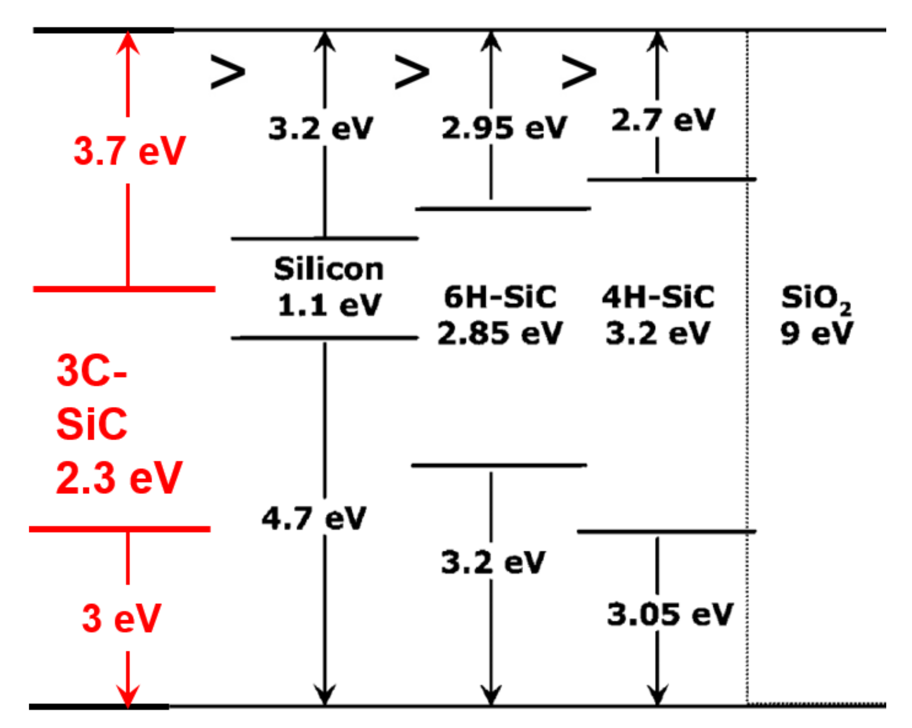
2. Cubic Silicon Carbide (3C-SiC): Structure and Material Properties for Power Electronic Application
3. Processing Technology for 3C-SiC
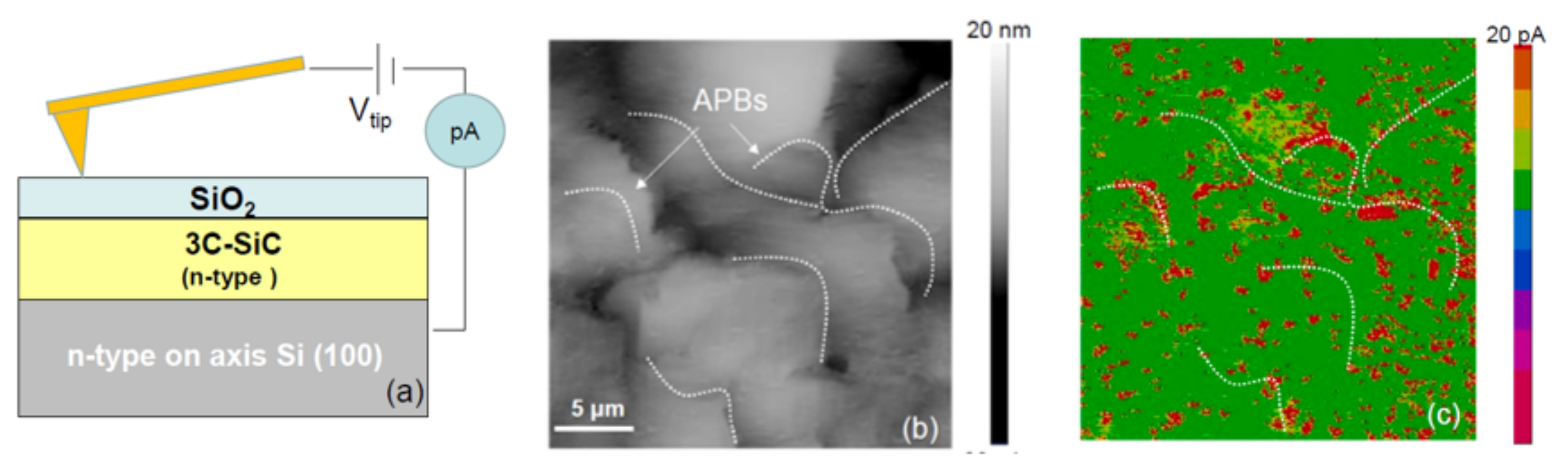
3.1. Schottky Contact

| Metal | 3C-SiC Orientation | Growing Substrate | Schottky Barrier Height (eV) | Ideality Factor | Extraction Method | Ref. |
|---|---|---|---|---|---|---|
| Au | 100 | Si | 1.15 | N.A. | C-V | [22] |
| Au | 100 | Si | 1.2 | 1.5 | C-V | [23] |
| Au | 111, 100 | Si | 1.0–1.6 | N.A. | C-V | [24] |
| Pt | 1.3–1.8 | |||||
| Pt | 100 | Si | 0.95 (as dep) −1.35 (800 °C) | N.A. | C-V | [25] |
| Pd | 100 | Si | 0.92, 0.95 | N.A. | C-V, XPS | [26] |
| Au | 0.87, 0.78 | |||||
| Co | 0.73, 0.69 | |||||
| Au | 100 | Si | 0.47–0.69 | 1.58–2.30 | I-V | [27] |
| Pd | 100 | Si | 0.42–0.60 | 3.02–5.28 | I-V | [28] |
| Ti | 100 | 3C-SiC | 0.4, N.A. | N.A. | I-V, C-V | [29] |
| Au | 0.67, 0.65 | |||||
| Ni | 0.56, 0.54 | |||||
| Au | 111 | 4H-SiC | 0.7, 1.39 | >2 | I-V, I-V by C-AFM | [19] |
| Pt | 100 | 3C-SiC | 0.77 (as dep) −1.12 (500 °C) | N.A. | [30] | |
| Au | 111 | 4H-SiC | 0.73–0.76 | N.A. | I-V by C-AFM | [31] |
3.2. Ion Implantation and Activation
3.3. Ohmic Contact
3.4. MOS Processing
4. 3C-SiC Device Prototypes
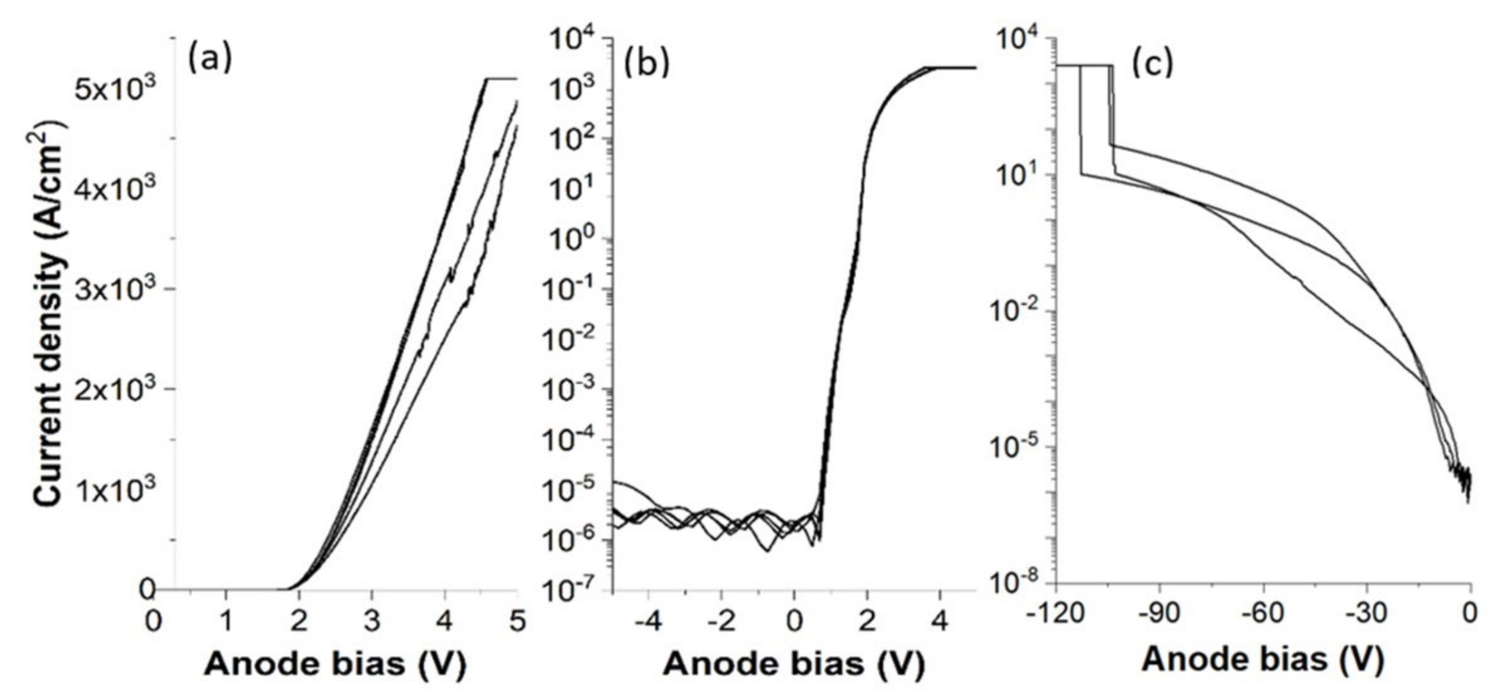
4.1. Schottky Diode
4.2. PiN Diode
4.3. MOSFET
5. Conclusions
Author Contributions
Funding
Institutional Review Board Statement
Informed Consent Statement
Data Availability Statement
Conflicts of Interest
References
- Roccaforte, F.; Greco, G.; Fiorenza, P.; Iucolano, F. An Overview of Normally-Off GaN-Based High Electron Mobility Transistors. Materials 2019, 12, 1599. [Google Scholar] [CrossRef] [PubMed] [Green Version]
- Tolbert, L.M.; King, T.; Ozpineci, B.; Campbell, J.; Muralidharan, G.; Rizy, D.; Sabau, A.; Zhang, H.; Zhang, W.; Xu, Y.; et al. Power Electronics for Distributed Energy Systems and Transmission and Distribution Applications: Assessing the Technical Needs for Utility Applications; U.S. Department of Energy Office of Scientific and Technical Information: Washington, DC, USA, 2005. [CrossRef] [Green Version]
- Yole Development. From Technologies to Markets: Compound Semiconductor Service Compound Montior; Quarterly Update—Q1 2020; Yole Development: Lyon, France, 2020. [Google Scholar]
- Ueda, T. Reliability Issues in GaN and SiC Power Devices. IEEE Int. Reliab. Phys. Symp. Proc. 2014, 1–6. [Google Scholar] [CrossRef]
- Gonzalez, J.O.; Wu, R.; Jahdi, S.; Alatise, O. Performance and Reliability Review of 650 v and 900 v Silicon and SiC Devices: MOSFETs, Cascode JFETs and IGBTs. IEEE Trans. Ind. Electron. 2020, 67, 7375–7385. [Google Scholar] [CrossRef] [Green Version]
- Chow, T.P.; Omura, I.; Higashiwaki, M.; Kawarada, H.; Pala, V. Smart Power Devices and ICs Using GaAs and Wide and Extreme Bandgap Semiconductors. IEEE Trans. Electron Devices 2017, 64, 856–873. [Google Scholar] [CrossRef]
- La Via, F.; Severino, A.; Anzalone, R.; Bongiorno, C.; Litrico, G.; Mauceri, M.; Schoeler, M.; Schuh, P.; Wellmann, P. From Thin Film to Bulk 3C-SiC Growth: Understanding the Mechanism of Defects Reduction. Mater. Sci. Semicond. Process. 2018, 78, 57–68. [Google Scholar] [CrossRef]
- Levinshein, M.; Sergey, L.; Shur, M. (Eds.) Properties of Advanced Semiconductor Materials: GaN, AIN, InN, BN, SiC, SiGe, 1st ed.; John Wiley & Sons, Inc.: New York, NY, USA, 2001. [Google Scholar]
- Lebedev, A.; Lebedev, S.; Dayvdov, V.; Novikov, S.; Makarov, Y. Growth and Investigation of SiC Based Herterostructures. In Proceedings of the 2016 15th Biennial Baltic Electronics Conference (BEC), Tallinn, Estonia, 3–5 October 2016; pp. 4–5. [Google Scholar]
- Arvanitopoulos, A.E.; Antoniou, M.; Perkins, S.; Jennings, M.; Guadas, M.B.; Gyftakis, K.N.; Lophitis, N. On the Suitability of 3C-Silicon Carbide as an Alternative to 4H-Silicon Carbide for Power Diodes. IEEE Trans. Ind. Appl. 2019, 55, 4080–4090. [Google Scholar] [CrossRef] [Green Version]
- Silicon Carbide Properties. Available online: https://www.ece.rutgers.edu/~jzhao/SiC-properties.html (accessed on 20 May 2021).
- Bimberg, D.; Altarelli, M.; Lipari, N.O. A Calculation of Valence Band Masses, Exciton and Acceptor Energies and the Ground State Properties of the Electron-Hole Liquid in Cubic SiC. Solid State Commun. 1981, 40, 437–440. [Google Scholar] [CrossRef]
- Fardi, H.; Van Zeghbroeck, B. Design and Simulation of 3C-SiC Vertical Power MOSFETs. Int. J. Electron. 2021, 108, 841–857. [Google Scholar] [CrossRef]
- Salupo, C.S.; Larkin, D.J.; Powell, J.A.; Matus, L.G. Electrical Properties of Epitaxial 3C- and 6H-SiC p-n Junction Diodes Produced Side-by-Side on 6H-SiC Substrates. IEEE Trans. Electron Devices 1994, 41, 826–835. [Google Scholar] [CrossRef]
- Spry, D.J.; Trunek, A.J.; Neudeck, P.G. High Breakdown Field P-Type 3C-SiC Schottky Diodes Grown on Step-Free 4H-SiC Mesas. In Silicon Carbide and Related Materials 2003; Materials Science Forum; Trans Tech Publications Ltd.: Bäch, Switzerland, 2004; Volume 457, pp. 1061–1064. [Google Scholar] [CrossRef]
- Tirino, L.; Weber, M.; Brennan, K.F.; Bellotti, E.; Goano, M. Temperature Dependence of the Impact Ionization Coefficients in GaAs, Cubic SiC, and Zinc-Blende GaN. J. Appl. Phys. 2003, 94, 423–430. [Google Scholar] [CrossRef]
- Bellotti, E.; Nilsson, H.-E.; Brennan, K.F.; Ruden, P.P. Ensemble Monte Carlo Calculation of Hole Transport in Bulk 3C–SiC. J. Appl. Phys. 1999, 85, 3211–3217. [Google Scholar] [CrossRef]
- Fardi, H.; Van Zeghbroeck, B. Breakdown Field Model for 3C-SiC Power Device Simulations. Mater. Sci. Forum 2018, 924, 617–620. [Google Scholar] [CrossRef]
- Eriksson, J.; Weng, M.H.; Roccaforte, F.; Giannazzo, F.; Leone, S.; Raineri, V. Toward an Ideal Schottky Barrier on 3C-SiC. Appl. Phys. Lett. 2009, 95, 81907. [Google Scholar] [CrossRef]
- Lanzia, M. (Ed.) Conductive Atomic Force Microscopy: Applications in Nanomaterials; Wiley VCH: Weinheim, Germany, 2017. [Google Scholar]
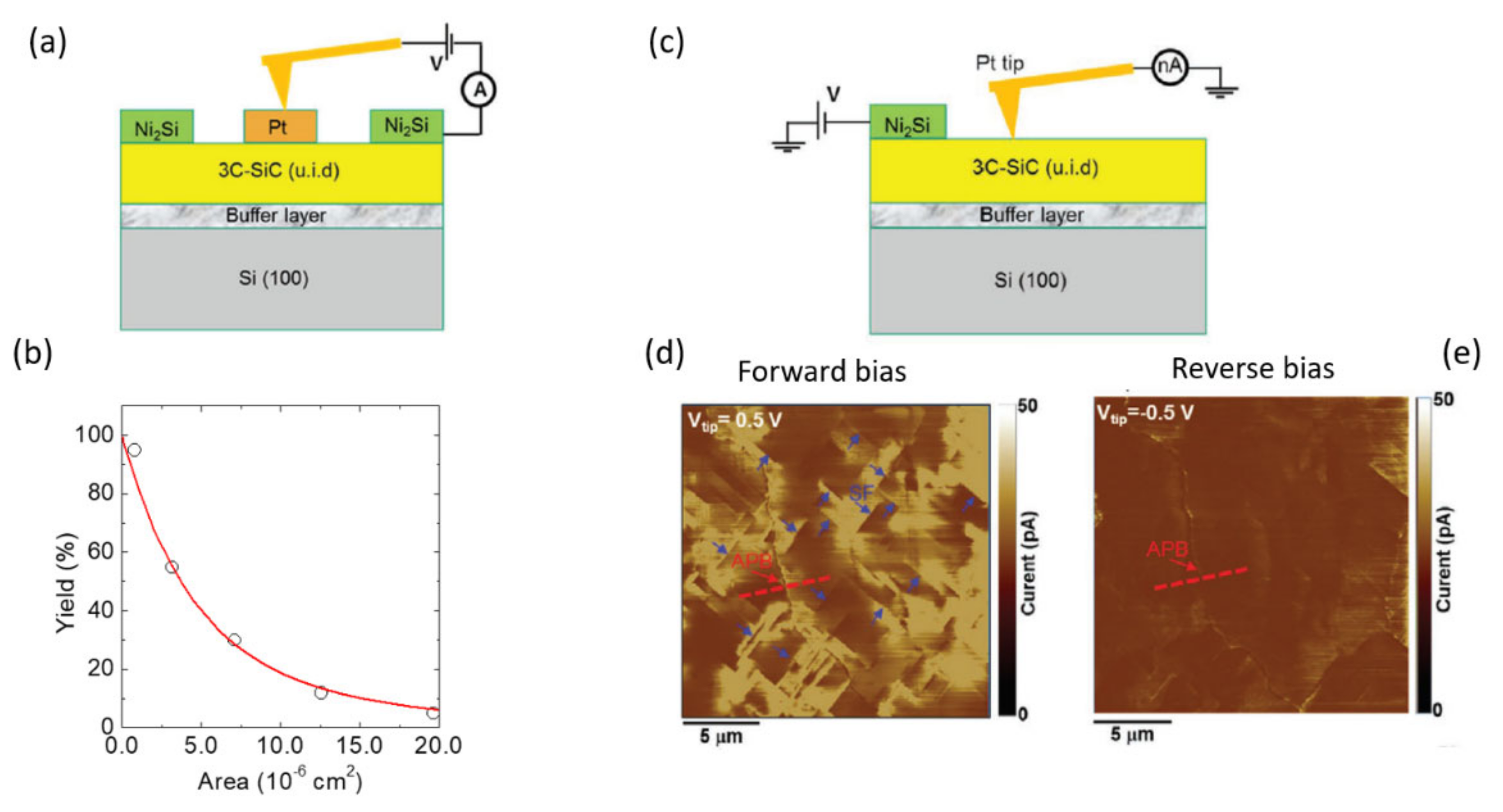
- Giannazzo, F.; Greco, G.; Di Franco, S.; Fiorenza, P.; Deretzis, I.; La Magna, A.; Bongiorno, C.; Zimbone, M.; La Via, F.; Zielinski, M.; et al. Impact of Stacking Faults and Domain Boundaries on the Electronic Transport in Cubic Silicon Carbide Probed by Conductive Atomic Force Microscopy. Adv. Electron. Mater. 2020, 6, 1–8. [Google Scholar] [CrossRef] [Green Version]
- Yoshida, S.; Sasaki, K.; Sakuma, E.; Misawa, S.; Gonda, S. Schottky Barrier Diodes on 3C-SiC. Appl. Phys. Lett. 1985, 46, 766–768. [Google Scholar] [CrossRef]
- Ioannou, D.E.; Papanicolaou, N.A.; Nordquist, P.E. The Effect of Heat Treatment on Au Schottky Contacts on β-SiC. IEEE Trans. Electron Devices 1987, 34, 1694–1699. [Google Scholar] [CrossRef]
- Fujii, Y.; Shigeta, M.; Furukawa, K.; Suzuki, A.; Nakajima, S. Dependence on the Schottky Metal and Crystal Orientation of the Schottky Diode Characteristics of Β-SiC Single Crystals Grown by Chemical Vapor Deposition. J. Appl. Phys. 1988, 64, 5020–5025. [Google Scholar] [CrossRef]
- Papanicolaou, N.A.; Christou, A.; Gipe, M.L. Pt and PtSix Schottky Contacts on N-type Β-SiC. J. Appl. Phys. 1989, 65, 3526–3530. [Google Scholar] [CrossRef]
- Waldrop, J.R.; Grant, R.W. Formation and Schottky Barrier Height of Metal Contacts to Β-SiC. Appl. Phys. Lett. 1990, 56, 557–559. [Google Scholar] [CrossRef]
- Constantinidis, G.; Kuzmic, J.; Michelakis, K.; Tsagaraki, K. Schottky Contacts on CF4/H2 Reactive Ion Etched β-SiC. Solid State Electron. 1998, 42, 253–256. [Google Scholar] [CrossRef]
- Roy, S.; Jacob, C.; Basu, S. Current Transport Properties of Pd/3C–SiC Schottky Junctions with Planar and Vertical Structures. Solid State Sci. 2004, 6, 377–382. [Google Scholar] [CrossRef]
- Satoh, M.; Matsuo, H. Evaluation of Schottky Barrier Height of Al, Ti, Au, and Ni Contacts to 3C-SiC. Mater. Sci. Forum 2006, 527, 923–926. [Google Scholar] [CrossRef]
- Eriksson, J.; Roccaforte, F.; Reshanov, S.; Giannazzo, F.; Lo Nigro, R.; Raineri, V. Evolution of the Electrical Characteristics of Pt/3C-SiC Schottky Contacts upon Thermal Annealing. AIP Conf. Proc. 2010, 1292, 75–78. [Google Scholar] [CrossRef]
- Alassaad, K.; Vivona, M.; Soulière, V.; Doisneau, B.; Cauwet, F.; Chaussende, D.; Giannazzo, F.; Roccaforte, F.; Ferro, G. Ge Mediated Surface Preparation for Twin Free 3C-SiC Nucleation and Growth on Low Off-Axis 4H-SiC Substrate. ECS J. Solid State Sci. Technol. 2014, 3, P285–P292. [Google Scholar] [CrossRef] [Green Version]
- Zhe, F. Silicon Carbide: Materials, Processing & Devices, 1st ed.; CRC Press: Boca Raton, FL, USA, 2003. [Google Scholar]
- Li, M.; Ahyi, A.C.; Zhu, X.; Chen, Z.; Isaacs-Smith, T.; Williams, J.R.; Crofton, J. Nickel Ohmic Contacts to N-Implanted (0001) 4H-SiC. J. Electron. Mater. 2010, 39, 540–544. [Google Scholar] [CrossRef]
- Vivona, M.; Greco, G.; Giannazzo, F.; Lo Nigro, R.; Rascunà, S.; Saggio, M.; Roccaforte, F. Thermal Stability of the Current Transport Mechanisms in Ni-Based Ohmic Contacts on n- and p-Implanted 4H-SiC. Semicond. Sci. Technol. 2014, 29, 75018. [Google Scholar] [CrossRef]
- Jones, K.A.; Wood, M.C.; Zheleva, T.S.; Kirchner, K.W.; Derenge, M.A.; Bolonikov, A.; Sudarshan, T.S.; Vispute, R.D.; Hullavarad, S.S.; Dhar, S. Structural and Chemical Comparison of Graphite and BN/AlN Caps Used for Annealing Ion Implanted SiC. J. Electron. Mater. 2008, 37, 917–924. [Google Scholar] [CrossRef]
- Frazzetto, A.; Giannazzo, F.; Nigro, R.L.; Raineri, V.; Roccaforte, F. Structural and Transport Properties in Alloyed Ti/Al Ohmic Contacts Formed on p-Type Al-Implanted 4H-SiC Annealed at High Temperature. J. Phys. D Appl. Phys. 2011, 44, 255302. [Google Scholar] [CrossRef] [Green Version]
- Jacob, C.; Pirouz, P.; Kuo, H.-I.; Mehregany, M. High Temperature Ohmic Contacts to 3C–Silicon Carbide Films. Solid State Electron. 1998, 42, 2329–2334. [Google Scholar] [CrossRef]
- Nipoti, R.; Canino, M.; Zielinski, M.; Torregrosa, F.; Carnera, A. 1300 °C Annealing of 1 × 10²⁰ °C m−3 Al + Ion Implanted 3C-SiC/Si. ECS J. Solid State Sci. Technol. 2019, 8, P480–P487. [Google Scholar] [CrossRef]
- Capano, M.A.; Ryu, S.; Cooper, J.A.; Melloch, M.R.; Rottner, K.; Karlsson, S.; Nordell, N.; Powell, A.; Walker, D.E. Surface Roughening in Ion Implanted 4H-Silicon Carbide. J. Electron. Mater. 1999, 28, 214–218. [Google Scholar] [CrossRef]
- Negoro, Y.; Katsumoto, K.; Kimoto, T.; Matsunami, H. Electronic Behaviors of High-Dose Phosphorus-Ion Implanted 4H-SiC (0001). J. Appl. Phys. 2004, 96, 224–228. [Google Scholar] [CrossRef] [Green Version]
- Vassilevski, K.V.; Wright, N.G.; Nikitina, I.P.; Horsfall, A.B.; O’Neill, A.G.; Uren, M.J.; Hilton, K.P.; Masterton, A.G.; Hydes, A.J.; Johnson, C.M. Protection of Selectively Implanted and Patterned Silicon Carbide Surfaces with Graphite Capping Layer during Post-Implantation Annealing. Semicond. Sci. Technol. 2005, 20, 271–278. [Google Scholar] [CrossRef]
- Song, X.; Biscarrat, J.; Michaud, J.-F.; Cayrel, F.; Zielinski, M.; Chassagne, T.; Portail, M.; Collard, E.; Alquier, D. Structural and Electrical Characterizations of N-Type Implanted Layers and Ohmic Contacts on 3C-SiC. Nucl. Instrum. Methods Phys. Res. Sect. B Beam Interact. Mater. Atoms 2011, 269, 2020–2025. [Google Scholar] [CrossRef]
- Bazin, A.E.; Michaud, J.F.; Autret-Lambert, C.; Cayrel, F.; Chassagne, T.; Portail, M.; Zielinski, M.; Collard, E.; Alquier, D. Ti–Ni Ohmic Contacts on 3C–SiC Doped by Nitrogen or Phosphorus Implantation. Mater. Sci. Eng. B 2010, 171, 120–126. [Google Scholar] [CrossRef]
- Song, X.; Bazin, A.E.; Michaud, J.F.; Cayrel, F.; Zielinski, M.; Portail, M.; Chassagne, T.; Collard, E.; Alquier, D. Electrical Characterization of Nitrogen Implanted 3C-SiC by SSRM and C TLM Measurements. Mater. Sci. Forum 2011, 679, 193–196. [Google Scholar] [CrossRef]
- Lee, K.Y.; Huang, Y.H.; Huang, C.F.; Chung, C.Y.; Lin, S.C.; Zhao, F. XRD Characterization for Al- and N-Doped 3C-SiC on Si (100) Substrate after Pulsed Excimer Laser Anneal. Mater. Sci. Forum 2012, 717, 497–500. [Google Scholar] [CrossRef]
- Taguchi, E.; Suzuki, Y.; Satoh, M. Electrical Properties of N Ion Implanted Layer in 3C-SiC(100) Grown on Self-Standing 3C-SiC Substrate. Mater. Sci. Forum 2007, 556, 579–582. [Google Scholar] [CrossRef]
- Khemka, V.; Patel, R.; Ramungul, N.; Chow, T.P.; Ghezzo, M.; Kretchmer, J. Characterization of Phosphorus Implantation in 4H-SiC. J. Electron. Mater. 1999, 28, 167–174. [Google Scholar] [CrossRef]
- Li, F.; Sharma, Y.; Shah, V.; Jennings, M.; Pérez-Tomás, A.; Myronov, M.; Fisher, C.; Leadley, D.; Mawby, P. Electrical Activation of Nitrogen Heavily Implanted 3C-SiC(100). Appl. Surf. Sci. 2015, 353, 958–963. [Google Scholar] [CrossRef] [Green Version]
- Rao, M.V.; Griffiths, P.; Holland, O.W.; Kelner, G.; Freitas, J.A.; Simons, D.S.; Chi, P.H.; Ghezzo, M. Al and B Ion-implantations in 6H- and 3C-SiC. J. Appl. Phys. 1995, 77, 2479–2485. [Google Scholar] [CrossRef]
- Nagasawa, H.; Abe, M.; Yagi, K.; Kawahara, T.; Hatta, N. Fabrication of High Performance 3C-SiC Vertical MOSFETs by Reducing Planar Defects. Phys. Status Solidi Basic Res. 2008, 245, 1272–1280. [Google Scholar] [CrossRef]
- La Via, F.; Mauceri, M.; Scuderi, V.; Calabretta, C.; Zimbone, M.; Anzalone, R. 3C-SiC Bulk Growth: Effect of Growth Rate and Doping on Defects and Stress. Mater. Sci. Forum 2020, 1004, 120–125. [Google Scholar] [CrossRef]
- Lossy, R.; Reichert, W.; Obermeier, E. Characterization of 3C-SiC Doped by Nitrogen Implantation. Mater. Sci. Eng. B 1997, 46, 156–159. [Google Scholar] [CrossRef]
- Lossy, R.; Reichert, W.; Obermeier, E.; Skorupa, W. Doping of 3C-SiC by Implantation of Nitrogen at High Temperatures. J. Electron. Mater. 1997, 26, 123–127. [Google Scholar] [CrossRef]
- Suzuki, Y.; Taguchi, E.; Nagata, S.; Satoh, M. Evaluation of Specific Contact Resistance of Al, Ti, and Ni Contacts to N Ion Implanted 3C-SiC(100). Mater. Sci. Forum 2007, 556, 705–708. [Google Scholar] [CrossRef]
- Song, X.; Biscarrat, J.; Bazin, A.E.; Michaud, J.F.; Cayrel, F.; Zielinski, M.; Chassagne, T.; Portail, M.; Collard, E.; Alquier, D. Dose Influence on Physical and Electrical Properties of Nitrogen Implantation in 3C-SiC on Si. Mater. Sci. Forum 2012, 711, 154–158. [Google Scholar] [CrossRef]
- Jennings, M.R.; Fisher, C.A.; Walker, D.; Sanchez, A.; Pérez-Tomás, A.; Hamilton, D.P.; Gammon, P.M.; Burrows, S.E.; Thomas, S.M.; Sharma, Y.K.; et al. On the Ti3SiC2 Metallic Phase Formation for Robust P-Type 4H-SiC Ohmic Contacts. Mater. Sci. Forum 2014, 778, 693–696. [Google Scholar] [CrossRef]
- Eriksson, J.; Roccaforte, F.; Giannazzo, F.; Lo Nigro, R.; Raineri, V.; Lorenzzi, J.; Ferro, G. Improved Ni/3C-SiC Contacts by Effective Contact Area and Conductivity Increases at the Nanoscale. Appl. Phys. Lett. 2009, 94, 112104. [Google Scholar] [CrossRef]
- Noh, J.I.; Nahm, K.S.; Kim, K.C.; Capano, M.A. Effect of Surface Preparation on Ni Ohmic Contact to 3C-SiC. Solid State Electron. 2002, 46, 2273–2279. [Google Scholar] [CrossRef]
- Moki, A.; Shenoy, P.; Alok, D.; Baliga, B.J.; Wongchotigul, K.; Spencer, M.G. Low Resistivity As-Deposited Ohmic Contacts to 3C-SiC. J. Electron. Mater. 1995, 24, 315–318. [Google Scholar] [CrossRef]
- Roy, S.; Jacob, C.; Basu, S. Ohmic Contacts to 3C-SiC for Schottky Diode Gas Sensors. Solid State Electron. 2003, 47, 2035–2041. [Google Scholar] [CrossRef]
- Bazin, A.E.; Michaud, J.F.; Cayrel, F.; Portail, M.; Chassagne, T.; Zielinski, M.; Collard, E.; Alquier, D. High Quality Ohmic Contacts on N-type 3C-SiC Obtained by High and Low Process Temperature. AIP Conf. Proc. 2010, 1292, 51–54. [Google Scholar] [CrossRef]
- Wan, J.; Capano, M.A.; Melloch, M.R. Formation of Low Resistivity Ohmic Contacts to N-Type 3C-SiC. Solid State Electron. 2002, 46, 1227–1230. [Google Scholar] [CrossRef]
- Zhang, J.; Howe, R.T.; Maboudian, R. Nickel and Platinum Ohmic Contacts to Polycrystalline 3C-Silicon Carbide. Mater. Sci. Eng. B 2007, 139, 235–239. [Google Scholar] [CrossRef]
- Chung, G.-S.; Yoon, K.-H. Ohmic Contacts to Single-Crystalline 3C-SiC Films for Extreme-Environment MEMS Applications. Microelectron. J. 2008, 39, 1408–1412. [Google Scholar] [CrossRef]
- Li, F.; Sharma, Y.; Walker, D.; Hindmarsh, S.; Jennings, M.; Martin, D.; Fisher, C.; Gammon, P.; Pérez-Tomás, A.; Mawby, P. 3C-SiC Transistor with Ohmic Contacts Defined at Room Temperature. IEEE Electron Device Lett. 2016, 37, 1189–1192. [Google Scholar] [CrossRef]
- Spera, M.; Greco, G.; Lo Nigro, R.; Bongiorno, C.; Giannazzo, F.; Zielinski, M.; La Via, F.; Roccaforte, F. Ohmic Contacts on N-Type and p-Type Cubic Silicon Carbide (3C-SiC) Grown on Silicon. Mater. Sci. Semicond. Process. 2019, 93, 295–298. [Google Scholar] [CrossRef] [Green Version]
- Jiang, Y.; Zhao, C.; Liu, S.; Huang, Q. Polysilicon-Al Based Ohmic Contact on p-Type 3C-SiC Film Grown on Silicon Substrate. In Proceedings of the 2006 8th Internation Conference on Solid-State and Integrated Circuit Technology Proceedings, Shanghai, China, 23–26 October 2006; pp. 938–940. [Google Scholar]
- Schöner, A.; Krieger, M.; Pensl, G.; Abe, M.; Nagasawa, H. Fabrication and Characterization of 3C-SiC-Based MOSFETs. Chem. Vap. Depos. 2006, 12, 523–530. [Google Scholar] [CrossRef]
- Afanas’ev, V.V.; Ciobanu, F.; Pensl, G.; Stesmans, A. Contributions to the Density of Interface States in SiC MOS Structures. In Silicon Carbide: Recent Major Advances; Choyke, W.J., Matsunami, H., Pensl, G., Eds.; Springer: Berlin/Heidelberg, Germany, 2004; pp. 343–371. [Google Scholar] [CrossRef]
- Afanasev, V.; Bassler, M.; Pensl, G.; Shulz, M. Intrinsic SiC/SiO2 Interface States. Phys. Stat. Sol. 1997, 162, 321–337. [Google Scholar] [CrossRef]
- Esteve, R. Fabrication and Characterization of 3C- and 4H-SiC MOSFETs. Doctoral Thesis, KTH, School of Information and Communication Technology (ICT), Integrated Devices and Circuits, Stockholm, Sweden, 2011. [Google Scholar]
- Esteve, R.; Schöner, A.; Reshanov, S.A.; Zetterling, C.-M.; Nagasawa, H. Comparative Study of Thermally Grown Oxides on N-Type Free Standing 3C-SiC (001). J. Appl. Phys. 2009, 106, 44513. [Google Scholar] [CrossRef]
- Wan, J.; Capano, M.A.; Melloch, M.R.; Cooper, J.A. N-Channel 3C-SiC MOSFETs on Silicon Substrate. IEEE Electron Device Lett. 2002, 23, 482–484. [Google Scholar] [CrossRef]
- Abe, M.; Nagasawa, H.; Ericsson, P.; Strömberg, H.; Bakowski, M.; Schöner, A. High Current Capability of 3C-SiC Vertical DMOSFETs. Microelectron. Eng. 2006, 83, 24–26. [Google Scholar] [CrossRef]
- Krieger, M.; Beljakowa, S.; Trapaidze, L.; Frank, T.; Weber, H.B.; Pensl, G.; Hatta, N.; Abe, M.; Nagasawa, H.; Schöner, A. Analysis of Interface Trap Parameters from Double-Peak Conductance Spectra Taken on N-Implanted 3C-SiC MOS Capacitors. Phys. Status Solidi Basic Res. 2008, 245, 1390–1395. [Google Scholar] [CrossRef]
- Li, F.; Vavasour, O.J.; Walker, M.; Martin, D.M.; Sharma, Y.K.; Russell, S.A.O.; Jennings, M.R.; Pérez-Tomás, A.; Mawby, P.A. Physical Characterisation of 3C-SiC(001)/SiO2 Interface Using XPS. Mater. Sci. Forum 2017, 897, 151–154. [Google Scholar] [CrossRef] [Green Version]
- Arora, R.; Rozen, J.; Fleetwood, D.M.; Galloway, K.F.; Zhang, C.X.; Han, J.; Dimitrijev, S.; Kong, F.; Feldman, L.C.; Pantelides, S.T.; et al. Charge Trapping Properties of 3C- and 4H-SiC MOS Capacitors With Nitrided Gate Oxides. IEEE Trans. Nucl. Sci. 2009, 56, 3185–3191. [Google Scholar] [CrossRef] [Green Version]
- Matocha, K.; Beaupre, R. Time-Dependent Dielectric Breakdown of Thermal Oxides on 4H-SiC. Mater. Sci. Forum 2007, 556, 675–678. [Google Scholar] [CrossRef]
- Fiorenza, P.; Schilirò, E.; Giannazzo, F.; Bongiorno, C.; Zielinski, M.; La Via, F.; Roccaforte, F. On the Origin of the Premature Breakdown of Thermal Oxide on 3C-SiC Probed by Electrical Scanning Probe Microscopy. Appl. Surf. Sci. 2020, 526, 146656. [Google Scholar] [CrossRef]
- Esteve, R.; Schöner, A.; Reshanov, S.A.; Zetterling, C.-M.; Nagasawa, H. Advanced Oxidation Process Combining Oxide Deposition and Short Postoxidation Step for N-Type 3C- and 4H-SiC. J. Appl. Phys. 2009, 106, 44514. [Google Scholar] [CrossRef]
- Anzalone, R.; Privitera, S.; Camarda, M.; Alberti, A.; Mannino, G.; Fiorenza, P.; Di Franco, S.; La Via, F. Interface State Density Evaluation of High Quality Hetero-Epitaxial 3C–SiC(001) for High-Power MOSFET Applications. Mater. Sci. Eng. B 2015, 198, 14–19. [Google Scholar] [CrossRef]
- Sharma, Y.K.; Li, F.; Jennings, M.R.; Fisher, C.A.; Pérez-Tomás, A.; Thomas, S.; Hamilton, D.P.; Russell, S.A.O.; Mawby, P.A. High-Temperature (1200–1400 °C) Dry Oxidation of 3C-SiC on Silicon. J. Electron. Mater. 2015, 44, 4167–4174. [Google Scholar] [CrossRef]
- Furukawa, K.; Uemoto, A.; Shigeta, M.; Suzuki, A.; Nakajima, S. 3C-SiC P-n Junction Diodes. Appl. Phys. Lett. 1986, 48, 1536–1537. [Google Scholar] [CrossRef]
- Davis, R.F.; Kelner, G.; Shur, M.; Palmour, J.W.; Edmond, J.A. Thin Film Deposition and Microelectronic and Optoelectronic Device Fabrication and Characterization in Monocrystalline Alpha and Beta Silicon Carbide. Proc. IEEE 1991, 79, 677–701. [Google Scholar] [CrossRef]
- Neudeck, P.G.; Larkin, D.J.; Starr, J.E.; Powell, J.A.; Salupo, C.S.; Matus, L.G. Greatly Improved 3C-SiC p-n Junction Diodes Grown by Chemical Vapor Deposition. IEEE Electron Device Lett. 1993, 14, 136–139. [Google Scholar] [CrossRef]
- Shenoy, P.; Moki, A.; Baliga, B.J.; Alok, D.; Wongchotigul, K.; Spencer, M. Vertical Schottky Barrier Diodes on 3C-SiC Grown on Si. In Proceedings of the 1994 IEEE International Electron Devices Meeting, San Francisco, CA, USA, 11–14 December 1994; pp. 411–414. [Google Scholar] [CrossRef]
- Cherkaoui, K.; Duane, R.; Ward, P.; Blake, A. Fabrication and Characterisation of Silicide/3C-SiC/Si Contacts for Schottky Barrier Diode Application. ECS Meet. Abstr. 2020, 23, 1334. [Google Scholar] [CrossRef]
- Arvanitopoulos, A.; Li, F.; Jennings, M.R.; Perkins, S.; Gyftakis, K.N.; Antoniou, M.; Mawby, P.; Lophitis, N. Experimental Investigation and Verification of Traps Affecting the Performance of 3C-SiC-on-Si Schottky Barrier Diodes. In Proceedings of the 2019 IEEE Energy Conversion Congress and Exposition (ECCE), Baltimore, MD, USA, 29 September–3 October 2019; pp. 1941–1947. [Google Scholar] [CrossRef]
- Wang, L.; Dimitrijev, S.; Han, J.; Tanner, P.; Iacopi, A.; Hold, L. Demonstration of P-Type 3C–SiC Grown on 150 mm Si(100) Substrates by Atomic-Layer Epitaxy at 1000 °C. J. Cryst. Growth 2011, 329, 67–70. [Google Scholar] [CrossRef] [Green Version]
- Shibahara, K.; Takeuchi, T.; Matsunami, H.; Nishino, S. Electrical Properties of Undoped and Ion-Implanted Cubic SiC Grown on Si(100) by Chemical Vapor Deposition. Jpn. J. Appl. Phys. 1989, 28, 1341–1347. [Google Scholar] [CrossRef]
- Tyagi, R.; Chow, T.P. Self-Enclosed vs. LOPOS-Terminated Lateral Planar p/Sup +/n and n/Sup +/p Junctions in 3C-SiC/Si. In Proceedings of the 8th International Symposium on Power Semiconductor Devices and Ics, ISPSD ’96 Proceedings, Lahaina, HI, USA, 20–23 May 1996; pp. 115–118. [Google Scholar] [CrossRef]
- Hatta, N.; Kawahara, T.; Yagi, K.; Nagasawa, H.; Reshanov, S.A.; Schöner, A. Reliable Method for Eliminating Stacking Fault on 3C-SiC(001). Mater. Sci. Forum 2012, 717, 173–176. [Google Scholar] [CrossRef]
- Fisicaro, G.; Bongiorno, C.; Deretzis, I.; Giannazzo, F.; La Via, F.; Roccaforte, F.; Zielinski, M.; Zimbone, M.; La Magna, A. Genesis and Evolution of Extended Defects: The Role of Evolving Interface Instabilities in Cubic SiC. Appl. Phys. Rev. 2020, 7, 21402. [Google Scholar] [CrossRef]
- Singh, R.; Cooper, J.A.; Melloch, M.R.; Chow, T.P.; Palmour, J.W. SiC Power Schottky and PiN Diodes. IEEE Trans. Electron Devices 2002, 49, 665–672. [Google Scholar] [CrossRef]
- Bu, Y.; Yoshimoto, H.; Watanabe, N.; Shima, A. Fabrication of 4H-SiC PiN Diodes without Bipolar Degradation by Improved Device Processes. J. Appl. Phys. 2017, 122, 244504. [Google Scholar] [CrossRef]
- Fisher, C.A.; Jennings, M.R.; Sharma, Y.K.; Hamilton, D.P.; Gammon, P.M.; Pérez-Tomás, A.; Thomas, S.M.; Burrows, S.E.; Mawby, P.A. Improved Performance of 4H-SiC PiN Diodes Using a Novel Combined High Temperature Oxidation and Annealing Process. IEEE Trans. Semicond. Manuf. 2014, 27, 443–451. [Google Scholar] [CrossRef]
- Bakowski, M.; Schöner, A.; Ericsson, P.; Stromberg, H.; Nagasawa, H.; Abe, M. Development of 3C-SiC MOSFETs. J. Telecommun. Inf. Tech. 2007, 2, 49–56. [Google Scholar]
- Japanese Push SiC Power. III-Vs Rev. 2004, 17, 35.
- Nagasawa, H.; Yagi, K.; Kawahara, T.; Hatta, N.; Abe, M.; Schöner, A.; Bakowski, M.; Ericsson, P.; Pensl, G. Challenges for Improving the Crystal Quality of 3C-SiC Verified with MOSFET Performance. Mater. Sci. Forum 2009, 600, 89–94. [Google Scholar] [CrossRef]
- Nagasawa, H.; Yagi, K.; Kawahara, T.; Hatta, N.; Abe, M. Hetero- and Homo-Epitaxial Growth of 3C-SiC for MOS-FETs. Microelectron. Eng. 2006, 83, 185–188. [Google Scholar] [CrossRef]
- Kobayashi, M.; Uchida, H.; Minami, A.; Sakata, T.; Esteve, R.; Schöner, A. 3C-SiC MOSFET with High Channel Mobility and CVD Gate Oxide. Mater. Sci. Forum 2011, 679, 645–648. [Google Scholar] [CrossRef]
- Schoner, A.; Bakowski, M.; Ericsson, P.; Stromberg, H.; Nagasawa, H.; Abe, M. Vertical MOSFET Devices Fabricated on 3C-SiC with High and Low Material Quality. MRS Online Proc. Libr. 2011, 911, 1303. [Google Scholar] [CrossRef]
- Lee, K.K.; Ishida, Y.; Ohshima, T.; Kojima, K.; Tanaka, Y.; Takahashi, T.; Okumura, H.; Arai, K.; Kamiya, T. N-Channel MOSFETs Fabricated on Homoepitaxy-Grown 3C-SiC Films. IEEE Electron Device Lett. 2003, 24, 466–468. [Google Scholar] [CrossRef]
- Uchida, H.; Minami, A.; Sakata, T.; Nagasawa, H.; Kobayashi, M. High Temperature Performance of 3C-SiC MOSFETs with High Channel Mobility. Mater. Sci. Forum 2012, 717, 1109–1112. [Google Scholar] [CrossRef]


| Material | Band Gap, (eV) | Intrinsic Carrier Conc., (cm−3) | Dielectric Constant | Electron Mobility (cm2/Vs) | Critical Electric Field (MV/cm) | Saturation Velocity (107 cm/s) | Thermal Conductivity (W/cmK) | Baliga Figure of Merit |
|---|---|---|---|---|---|---|---|---|
| Si | 1.12 | 1.5 × 10¹⁰ | 11.8 | 1350 | 0.2 | 1.0 | 1.5 | 1 |
| GaAs | 1.42 | 1.8 × 10⁶ | 13.1 | 8500 | 0.4 | 1.2 | 0.55 | 29 |
| 3C-SiC | 2.36 | 1.5 × 10⁻¹ | 9.7 | 800 | 1.4 | 2.5 | 3.2 | 86 |
| 4H-SiC | 3.26 | 8.2 × 10⁻⁹ | 10 | 720 a 650 c | 2.8 | 2.0 | 4.5 | 556 |
| 2H-GaN | 3.39 | 1.9 × 10⁻¹⁰ | 9.9 | 1000 a 2000 ** | 3.75 a 3.3 * | 2.5 | 1.3 | 3175 |
| Ga2O3 | 4.85 | 2.6 × 10⁻⁹ −1.0 × 10⁻²² | 10 | 300 | 8 | 1.8–2.0 | 0.1–0.3 | 6171 |
| Diamond | 5.45 | 1.6 × 10⁻²⁷ | 5.5 | 3800 | 10 | 2.7 | 22 | 8.4 × 10⁴ |
| 2H-AlN | 6.2 | 10−34 | 8.5 | 300 | 12 * | 1.7 | 2.85 | 1.8 × 10⁴ |
| Material | Implantation | PIA | Activation Rate | Ref. |
|---|---|---|---|---|
| N-Type | ||||
| 2 × 1017 cm−3 p-type 3C-SiC(100)/Si | RT 1, N, peak 5 × 10¹⁹/5 × 1020 cm−3 | None | 0.44%/0.55% | [52] |
| 400 °C, N, peak 5 × 1019 cm−3 | 1.35% | |||
| 800 °C, N, peak 5 × 10¹⁹/5 × 1020cm−3 | 15%/50.8% | |||
| 1 × 1018 cm−3 p-type 3C-SiC(100)/Si | 800 °C, N, peak 5 × 1019 cm−3 | None | 12.4% | [53] |
| 900 °C, N, peak 5 × 1019 cm−3 | 14.8% | |||
| 1000 °C, N, peak 5 × 1019 cm−3 | 18.4% | |||
| 1100 °C, N, peak 5 × 1019 cm−3 | 36.0% | |||
| 1200 °C, N, peak 5 × 1019 cm−3 | 52.2% | |||
| 1 × 1016 cm−3 p-type 3C-SiC(100) | RT, N, peak 1 × 1020 cm−3 | 10 min in Ar at 1500 °C | 68% | [49] |
| 1 × 1016 cm−3 p-type 3C-SiC(100) | RT, N, peak 6 × 1019 cm−3 | 10 min in Ar at 1400 °C | 80% | [54] |
| <1 × 1016 cm−3 n-type 3C-SiC(100)/Si | RT, N, peak 5 × 1020 cm−3 | 1 h in Ar at 1150 °C | 6.5% | [46] |
| 1 h in Ar at 1350 °C | 13% | |||
| <1 × 1016 cm−3 n-type 3C-SiC(100)/Si | RT, N, peak 5 × 1019 cm−3 | 1 h in Ar at 1150 °C | 40% | [44] |
| 1 h in Ar at 1350 °C | 57% | |||
| 1 h in Ar at 1400 °C | 100% | |||
| <1 × 1016 cm−3 n-type 3C-SiC(100/Si | RT, N, peak 5 × 10¹⁹/5 × 1020 cm−3 | 1 h in Ar at 1350 °C | 60%/17% | [55] |
| <1 × 1016 cm−3 n-type 3C-SiC(100/Si | RT, N, peak 1.5 × 10¹⁹/6 × 1020 cm−3 | 1 h in Ar at 1375 °C | 100%/12% | [49] |
| P-type | ||||
| 2.8 × 1016 cm−3 n-type 3C-SiC(100)/Si | RT and 850 °C, Al and B, peak 5 × 10¹⁹–1 × 1020 cm−3 | 10 min in N2 at 1200 °C | Too low, n-type behaviour | [50] |
| <1 × 1016 cm−3 n-type 3C-SiC(100)/Si | 500 °C, Al, peak 1 × 1020 cm−3 | 317–546 h in Ar at 1300 °C | Weak p-type behaviour | [38] |
| Contact | Doping (cm−3) | PMA Conditions | ρc (Ωcm2) | Ref. |
|---|---|---|---|---|
| N-Type | ||||
| Al | 5 × 10¹⁸ N implanted | As-deposited | 1 × 10⁻⁴ | [59] |
| 3 × 10¹⁹ N implanted | 6 × 10⁻⁵ | |||
| 1 × 10²⁰ N implanted | 5 × 10⁻⁵ | |||
| 3 × 10²⁰ N implanted | 1.3 × 10⁻⁵ | |||
| 6 × 10¹⁹ N implanted | As-deposited/500 °C | 5 × 10⁻⁷/6 × 10−5 | [54] | |
| 6 × 10¹⁸ N implanted | 300 °C | 5 × 10⁻⁷ | [61] | |
| 1 × 10¹⁷ N doped epi | As deposited/500 °C | 2 × 10⁻⁴/1 × 10−4 | [37] | |
| Ti | 5 × 10¹⁸ N implanted | As-deposited | 7 × 10⁻⁵ | [59] |
| 3 × 10¹⁹ N implanted | 4 × 10⁻⁵ | |||
| 1 × 10²⁰ N implanted | 2 × 10⁻⁵ | |||
| 3 × 10²⁰ N implanted | 1.5 × 10⁻⁵ | |||
| 6 × 10¹⁹ N implanted | As-deposited/500 °C | 5 × 10⁻⁶/6 × 10−5 | [54] | |
| Ni | Not known, N doped epi | 1000°C | 3.7 × 10⁻⁴ | [58] |
| 6 × 10¹⁹ N implanted | As-deposited/500 °C | 2 × 10⁻⁵/5 × 10−6 | [54] | |
| 3 × 10¹⁹ N doped epi | 950 °C | 1.2 × 10⁻⁵ | [61] | |
| 1 × 10¹⁷ N doped epi | As-deposited/500 °C | 5 × 10⁻⁴/5 × 10−5 | [37] | |
| 1 × 10²⁰ P implanted | 1000 °C | 1.4 × 10⁻⁵ | [61] | |
| Not known, poly crystal epi | As-deposited | 1.6 × 10⁻⁶ | [65] | |
| 5 × 10¹⁷ N doped epi | 950 °C | 1.5 × 10⁻⁵ | [57] | |
| 1 × 10¹⁷ N doped epi | 950 °C | 3.7 × 10⁻³ | [66] | |
| Ni/Ti | 5 × 10¹⁹ N implanted | As-deposited | 7 × 10⁻⁴ | [65] |
| 5 × 10²⁰ N implanted | 3 × 10⁻⁵ | |||
| 1 × 10¹⁹ N implanted | 1000 °C | 2 × 10⁻⁴ | ||
| 5 × 10¹⁹ N implanted | 4 × 10⁻⁵ | |||
| 5 × 10²⁰ N implanted | 9 × 10⁻⁶ | |||
| 5 × 10²⁰ N implanted | 1000 °C | 8 × 10⁻⁶ | [43] | |
| 5 × 10²⁰ P implanted | 2 × 10⁻⁵ | |||
| >1020 N implanted | 1050 °C | 2 × 10⁻⁵ | [61] | |
| 5 × 10¹⁹ N implanted | 1000 °C | 3.2 × 10⁻⁶ | [55] | |
| Au/Ti | 3 × 10²⁰ N implanted | 600 °C | 1.2 × 10⁻⁵ | [61] |
| Pt | Not know, poly crystal N doped epi | As-deposited | 1.2 × 10⁻⁵ | [63] |
| W | 1 × 10¹⁷ N doped epi | As-deposited/500 °C | 2 × 10⁻³/2 × 10−3 | [37] |
| TiW | Not know, N doped epi | 1000 °C | 4.6 × 10⁻⁴ | [64] |
| 4 × 10¹⁹ N/P implanted | As-deposited | ohmic | [68] | |
| P-type | ||||
| Al | 1.33 × 10¹⁷ Al doped epi | 710 °C | 1.4 × 10⁻² | [67] |
| Al/Poly | 3.5 × 10⁻⁴ | |||
| Ni/Al/Ti | 5 × 10¹⁹ Al doped epi | 950 °C | 1.8 × 10⁻⁵ | [66] |
| 1 × 10²⁰ Al implanted | 1000 °C | 10−2 | [38] | |
| 1 × 10²⁰ Al implanted | 1000 °C | 10−3 | This work | |
| Oxidation Substrate | Oxidation | POA | Qfc (cm−2) | Dit (cm−2 eV−1) | Ec (MV/cm) | Ref. |
|---|---|---|---|---|---|---|
| n-type 3C-SiC | NO, 1175 °C, 4 h | - | - | ~1011 | - | [68] |
| Al implanted 3C-SiC | Dry O2, 1100 °C, 1.5 h | Wet O2, 950 °C, 3 h | - | 5 × 10¹²–1 × 10¹³ | - | [74] |
| n-type 3C-SiC | Dry O2, 1120 °C, 0.5 h | Ar, 1120 °C, 1 h | - | ~1012 | - | [75] |
| n-type 3C-SiC | PECVD (SiH4 + N2O) | N2O, 1100 °C, 3 h | 2.01 × 10¹² | ~1012 | 8.2 | [80] |
| Wet O2, 950 °C, 3 h | 1.7 × 10¹¹ | ~2 × 10¹² | 9.1 | |||
| Dry O2, 950 °C, 3 h | 1.76 × 10¹¹ | ~2 × 10¹³ | 5.9 | |||
| N2, 1100 °C, 3 h | 4.65 × 10¹² | ~7 × 10¹² | 6.3 | |||
| N2, 950 °C, 3 h | 2.63 × 10¹² | ~2 × 10¹³ | 6.2 | |||
| n-type 3C-SiC | NO, 1185 °C, 2 h | - | - | ~1012 | - | [77] |
| N2O, 1185 °C, 1 h | - | - | ~8 × 10¹¹ | - | ||
| n-type 3C-SiC | Dry O2, 1100 °C, 4 h | - | 9.3 × 10¹² | 4.27 × 10¹³ | - | [73] |
| Dry O2, 1200 °C, 1 h | - | 7.1 × 10¹² | 6.59 × 10¹³ | - | ||
| Dry O2, 1100 °C, 1.5 h | O2, 950 °C, 3 h | 1.3 × 10¹² | 7.1 × 10¹² | - | ||
| Dry O2, 1100 °C, 1.5 h | Wet O2, 950 °C, 3 h | 0.9 × 10¹² | 5.2 × 10¹² | - | ||
| N2O, 1200 °C, 2 h | - | 3.0 × 10¹² | 1.15 × 10¹³ | - | ||
| N2O, 1250 °C, 2 h | 3.1 × 10¹² | 9.1 × 10¹² | - | |||
| N2O, 1250 °C, 2 h | Wet O2, 950 °C, 3 h | 1.6 × 10¹² | 9.4 × 10¹² | - | ||
| n-type 3C-SiC | PECVD (SiH4 + N2O) | N2, 950 °C | 5.7–7 × 10¹² | 5 × 10¹¹–7 × 10¹² | - | [81] |
| n-type 3C-SiC | Dry O2, 1200 °C | - | 1.1 × 10¹² | ~1012 | - | [82] |
| Dry O2, 1300 °C | 1.1 × 10¹² | |||||
| Dry O2, 1400 °C | 4.1 × 10¹² |
| Structure | Channel | Oxidation | POA | µFE (cm2/V.s) | BV (V) | Ref. |
|---|---|---|---|---|---|---|
| Lateral | 2 × 1017 cm−3 p-type epi | Wet O2, 1150 °C, 2.5 h | Ar, 1150 °C, 0.5 h + Wet O2, 950 °C, 2 h | ≈165 | - | [73] |
| Lateral | 1 × 1016 cm−3 p-type epi | Wet O2, 1100 °C | Ar, 1150 °C, 0.5 h + Wet O2, 800 °C, 0.5 h | ≈229 | - | [103] |
| Lateral | 1 × 1018 cm−3 Al implanted | Dry O2, 1300 °C | - | ≈80 | - | [65] |
| Vertical | 1 × 1018 cm−3 Al implanted | Dry O2, 1100 °C, 1.5h | Wet O2, 950 °C, 3 h | ≈28 | ≈100 | [68] |
| Vertical | 1 × 1018 cm−3 Al implanted | Dry O2, 1100 °C, 1.5 h | Wet O2, 950 °C, 3 h | ≈45 | 550–600 | [50] |
| Vertical | Al implanted | Wet O2, 1150 °C, | - | >100 | [104] |
Publisher’s Note: MDPI stays neutral with regard to jurisdictional claims in published maps and institutional affiliations. |
© 2021 by the authors. Licensee MDPI, Basel, Switzerland. This article is an open access article distributed under the terms and conditions of the Creative Commons Attribution (CC BY) license (https://creativecommons.org/licenses/by/4.0/).
Share and Cite
Li, F.; Roccaforte, F.; Greco, G.; Fiorenza, P.; La Via, F.; Pérez-Tomas, A.; Evans, J.E.; Fisher, C.A.; Monaghan, F.A.; Mawby, P.A.; et al. Status and Prospects of Cubic Silicon Carbide Power Electronics Device Technology. Materials 2021, 14, 5831. https://doi.org/10.3390/ma14195831
Li F, Roccaforte F, Greco G, Fiorenza P, La Via F, Pérez-Tomas A, Evans JE, Fisher CA, Monaghan FA, Mawby PA, et al. Status and Prospects of Cubic Silicon Carbide Power Electronics Device Technology. Materials. 2021; 14(19):5831. https://doi.org/10.3390/ma14195831
Chicago/Turabian StyleLi, Fan, Fabrizio Roccaforte, Giuseppe Greco, Patrick Fiorenza, Francesco La Via, Amador Pérez-Tomas, Jonathan Edward Evans, Craig Arthur Fisher, Finn Alec Monaghan, Philip Andrew Mawby, and et al. 2021. "Status and Prospects of Cubic Silicon Carbide Power Electronics Device Technology" Materials 14, no. 19: 5831. https://doi.org/10.3390/ma14195831
APA StyleLi, F., Roccaforte, F., Greco, G., Fiorenza, P., La Via, F., Pérez-Tomas, A., Evans, J. E., Fisher, C. A., Monaghan, F. A., Mawby, P. A., & Jennings, M. (2021). Status and Prospects of Cubic Silicon Carbide Power Electronics Device Technology. Materials, 14(19), 5831. https://doi.org/10.3390/ma14195831