
A Short Review on Various Engineering Applications of Electrospun One-Dimensional Metal Oxides


Department of Engineering Materials and Biomaterials, Faculty of Mechanical Engineering, Silesian University of Technology, 44-100 Gliwice, Poland
*
Author to whom correspondence should be addressed.
Materials 2021, 14(18), 5139; https://doi.org/10.3390/ma14185139
Submission received: 27 July 2021
/
Revised: 1 September 2021
/
Accepted: 3 September 2021
/
Published: 7 September 2021
(This article belongs to the Special Issue State-of-the-Art Materials Science in Poland (2020–2022))
Abstract
:The growing scientific interest in one-dimensional (1D) nanostructures based on metal-oxide semiconductors (MOS) resulted in the analysis of their structure, properties and fabrication methods being the subject of many research projects and publications all over the world, including in Poland. The application of the method of electrospinning with subsequent calcination for the production of these materials is currently very popular, which results from its simplicity and the possibility to control the properties of the obtained materials. The growing trend of industrial application of electrospun 1D MOS and the progress in modern technologies of nanomaterials properties investigations indicate the necessity to maintain the high level of research and development activities related to the structure and properties analysis of low-dimensional nanomaterials. Therefore, this review perfectly fits both the global trends and is a summary of many years of research work in the field of electrospinning carried out in many research units, especially in the Department of Engineering Materials and Biomaterials of the Faculty of Mechanical Engineering and Technology of Silesian University of Technology, as well as an announcement of further activities in this field.
1. Introduction
One of the main streams of materials engineering in Poland and worldwide, on which the attention of not only the scientific community but also the industry is currently focused, are nanomaterials and methods of their fabrication. This interest is not unfounded because nanomaterials exhibit much more favorable mechanical properties compared to those presented by traditional materials and outstanding physicochemical properties due to their large specific surface area and quantum effects observed at the nanometer scale [1,2,3]. Nanomaterials in terms of the number of dimensions that remain below 100 nm can be classified as follows: zero-dimensional (0D), one-dimensional (1D), two-dimensional (2D) and three-dimensional (3D) (Figure 1) [4,5].
Each of the above-mentioned groups of materials has a huge application potential in almost all industrial fields, especially in those that require a constant search for new solutions and technologies to ensure a high quality of manufactured products. However, in the last two decades, one-dimensional nanoobjects seem to have stood out in popularity over the other types of nanomaterials, which is due to their quantum-confined structure determining unique optical, electrical, magnetic and thermoelectric properties [6]. This feature makes it possible to obtain the desired properties by controlling the size of the nanostructure [7,8,9]. The number of publications shows that the most commonly fabricated and studied one-dimensional nanomaterials for three decades continuously included nanotubes, especially carbon nanotubes, while 1D nanostructures in the form of nanofibers and nanowires have definitely been less popular so far (Figure 2). Not only worldwide but also in Poland, the great potential of 1D nanomaterials is recognized, which can be inferred by analyzing data from the Polish National Science Center (NCN), which indicate that over the past decade, NCN has funded over 400 projects in this area and currently 12 such studies are being completed.
Due to the strongest quantum effect among various one-dimensional nanomaterials, it is metal oxide semiconductor nanostructures that are most often studied for applications in the development of modern solar cells, optoelectronic and acoustic devices, liquid crystal devices and detectors. To date, researchers have devoted the most attention to ZnO, TiO2, SiO2 and Bi2O3. However, there are increasing publications on other 1D metal oxides, including In2O3 and SnO2 [10,11,12,13,14,15,16,17,18,19,20,21,22,23,24,25,26,27,28,29,30]. According to recent scientific reports, these types of materials represent the future of semiconductor-based devices, so it is important to focus on their development and on selecting the most advantageous method for their fabrication. To date, many methods have been developed for the fabrication of one-dimensional nanomaterials, including chemical and physical vapor deposition methods (CVD and PVD), salt and hydrothermal methods, controlled growth from liquid phase (VLS), matrix synthesis, nanolithography or electrospinning from solution [15,20,31,32,33,34,35,36,37,38,39,40,41,42,43,44,45,46,47,48,49,50,51,52,53,54]. Nevertheless, the last mentioned method has a particular advantage over the others. Electrospinning allows the production of materials not only on a laboratory scale, but also on an industrial scale through the modifications, such as use of multineedle or needle-less processes. Moreover, it does not require a complicated apparatus (Figure 3) or expensive precursors, and allows the control of the morphology and properties of the obtained products with only a few parameters. It is worth noting that, unlike PVD and CVD methods, this technique also does not require a protective atmosphere to manufacture uncontaminated, pure nanomaterial. Thus, the nanostructures obtained by this method are ready for use without further functionalization or purification. Electrospinning in combination with subsequent high-temperature processing enables producing high quality oxide one-dimensional nanostructures in an uncomplicated way with the desired properties, among others [10,11,31,35,48,51,55,56,57,58,59,60,61,62,63].
The great importance of the electrospinning method in the manufacturing of one-dimensional nanomaterials of all types is confirmed by numerous projects carried out in Polish research units and financed by the National Science Center. According to information obtained from the NCN website, 11 out of 24 projects using electrospinning as the main method of manufacturing research objects are currently being carried out (Table 1). The majority of grants awarded concerned the potential application of 1D nanostructures in medicine, while the remaining ones concerned photovoltaics, catalysis and purification of the water environment. The popularity of this method in Poland is also confirmed by the number of publications originating from Polish institutions. According to the Scopus database, more than 500 Polish scientific articles have been published to date, most of which come from the Department of Engineering Materials and Biomaterials (T. Tański and W. Matysiak in cooperation with W. Smok, M. Zaborowska and P. Jarka), the Institute of Physics (T. Błachowicz), the Silesian University of Technology, the Institute of Fundamental Technological Research, the Polish Academy of Sciences (P. Sajkiewicz), the International Center of Electron Microscopy for Material Science, AGH University of Science and Technology (Z.J. Krysiak, U. Stachewicz) and the Materials Design Division, Warsaw University of Technology (W. Święszkowski). These data confirm how high the expectations and hopes are for the development of this manufacturing method.
A research group from the Department of Engineering Materials and Biomaterials is in the process of implementing the NSC project entitled ‘‘New polymer structures for the construction of photovoltaic cells’’ based on the fabrication of nanostructures from ZnO and TiO2 [10,59,64,65,66]; in addition, one member of the group is pursuing a Diamond Grant entitled “Hybrid one-dimensional nanostructures X (X = ZnO and/or TiO2)-Yb3+/Eu3+ obtained by hybrid methods with enhanced photocatalytic activity”.

Table 1.
The 11 projects financed by National Science Centre on one-dimensional nanomaterials that are currently implemented in Polish scientific units.
Table 1.
The 11 projects financed by National Science Centre on one-dimensional nanomaterials that are currently implemented in Polish scientific units.
| No. | Project Title | Scientific Unit | Status | Research Object | Ref. |
|---|---|---|---|---|---|
| 1 | The use of collagen for surface functionalization using chemical methods of polycaprolactone nanofibers formed by the electrospinning technique | Institute of Fundamental Technological Research, Polish Academy of Sciences | Current 10 July 2017 09 July 2021 | Manufacturing of three types of nanofibers from various aliphatic polysters—poly (caprolactone), poly (L-lactide) and their copolymer and functionalization of their surface. | [67] |
| 2 | New polymer structures for the construction of photovoltaic cells | University of Silesia in Katowice, Faculty of Science and Technology, Silesian University of Technology, Faculty of Mechanical Engineering | Current 11 October 2017 10 June 2021 | Preparation of composites containing a dispersed phase in the form of a conductive polymer or inorganic ZnO and TiO2 nanoparticles or hybrid systems made of these fillers and optical properties analysis. | [68] |
| 3 | Innovative biocatalytic systems produced by the immobilization of enzymes on multifunctional materials synthesized by electrospinning | Poznan University of Technology, Faculty of Chemical Technology | Current 01 March 2019 28 February 2022 | The use of materials produced by the electrospinning method for the immobilization of selected enzymes of environmental importance and the application of the obtained biocatalytic systems in the processes of dye degradation. | [69] |
| 4 | Multifunctional composite materials enriched with natural polyphenols for potential applications in tissue engineering | AGH University of Science and Technology, Faculty of Materials Science and Ceramics | Current 22 October 2018 21 October 2022 | Design and production of new, multifunctional, bioresorbable composites enriched with polyphenols (PPh) obtained from medicinal plants (sage/rosemary) and individual polyphenolic compounds (rosmarinic acid and carnosic acid). | [70] |
| 5 | Thermosensitive hydrogels filled with bioactive nanofibers for regeneration of neural tissue | Institute of Fundamental Technological Research, Polish Academy of Sciences | Current 21 January 2019 20 January 2022 | Design and manufacturing of a smart, injectable hydrogel, loaded with short electrospun, bioactive PLLA and laminin nanofibers for central nervous system tissue engineering. | [71] |
| 6 | Cellular responses to the properties of electrospun polymer fibers for tissue engineering applications | AGH University of Science and Technology, International Centre of Electron Microscopy for Materials Science | Current 05 February 2020 04 February 2023 | Determining the relationship between the conductive and structural properties of polymer electrospun tissue scaffolds and cell growth for regenerative medicine applications. | [72] |
| 7 | Removal of selected environmental pollutants from water solutions with the use of immobilized laccase | Poznan University of Technology, Faculty of Chemical Technology | Current 20 August 2020 30 September 2021 | Development of a methodology for the production of new carriers in the form of electrospun nanofibers and membranes in the immobilization of enzymes, and then the use of immobilized enzyme systems in the remediation of phenolic compounds from aqueous solutions. | [73] |
| 8 | Nanofibrous mucoadhesive carrier of brinzolamide based on hydroxypropyl cellulose and β-cyclodextrin. | Institute of Fundamental Technological Research, Polish Academy of Sciences | Current 09 July 2020 08 July 2023 | Optimization of the chemical composition and production conditions of a modern nanofiber material intended for the gradual local release of an ophthalmic drug. | [74] |
| 9 | Investigation of the properties of the nature-inspired polymer nanofiber networks in the context of their application for water recovery and energy generation | AGH University of Science and Technology, Faculty of Materials Science and Ceramics | Current 01 September 2016 28 February 2022 | Understanding the process of wetting nanofibers due to their properties and using this knowledge to increase the efficiency of the process of collecting water from the fog, by incorporating nanofibers into the currently used Fog Water Collectors. | [75] |
| 10 | Bioactive materials capable of mimicking the state of hypoxia with high osteogenic and angiogenic potential | Jagiellonian University in Kraków, Faculty of Chemistry | Current 02 October 2019 01 October 2022 | Production of scaffolding containing particles of bioactive glasses modified with transition metal ions by electrospinning. | [76] |
| 11 | Electrical properties and catalytic activity against I-/I3-pair redox reactions of hierarchical carbon nanostructures with a new Ni-Co bimetallic catalyst | AGH University of Science and Technology, Faculty of Materials Science and Ceramics | Current 20 February 2020 19 February 2022 | Synthesis of hierarchical composites based on electrospun carbon nanofibers and metallic nanoparticles and their catalytic properties. | [77] |
2. Electrospinning of Metal Oxides 1D Nanostructures
The electrospinning technique has been known and used for nearly three decades. It involves the use of an electrostatic field created between electrodes (nozzle and collector) under the influence of high voltage to form and stretch a droplet of spinning solution into a fiber settling in a spiral motion on the collector, resulting in a fibrous (nano)mat [78,79,80,81,82,83,84]. The fibers obtained by this method are characterized by their nanometric diameter and considerable length, reaching up to several meters, and their structure, morphology and properties can be controlled by the parameters used, which can be divided into 3 groups (Figure 4) [84].
In the case of fabrication of metal oxide-based nanostructures, the electrospinning process is only an intermediate step, followed by temperature treatment (calcination) of the spun nanofibers to remove the polymer matrix. The entire fabrication process is shaped as follows: in the first stage (Stage 1, Figure 5), it is necessary to prepare a spinning solution, containing a given polymer (for each type of experiment, an appropriate polymer is selected each time, for example, it can be polyvinylpyrrolidone (PVP), polyacrylonitrile (PAN) or poly(vinyl alcohol)) (PVA) ensuring appropriate viscosity and precursor molecules (these are most often metal chlorides or nitrates) (Table 2).
Then, the homogeneous solution (the time and temperature of the homogenization process are experimentally chosen for each solution individually) is placed in the device pump from where it is fed through feed channels to the nozzle, where it is subjected to electrostatic field forces to form polymer/precursor composite nanofibers (Stage 2 Figure 5), which takes place due to solvents (e.g., ethanol (EtOH), N,N-Dimethyloformamide (DMF)) evaporation. To obtain the final product, which is 1D MOS, the spun polymer-precursor nanofibers are calcined until the organic phase is completely removed and nanostructures based on one or more oxides or with other dopant material are formed (Stage 3 Figure 5). Figure 6 shows the morphology and structure of SnO2 and In2O3 nanowires formed as a result of calcination of polymer/precursor nanofibers (Figure 6a,b) at a temperature of 500 °C, which are the subject of research by the research group from the Department of Engineering Materials and Biomaterials. Smooth, continuous, free from structural defects, polymer/precursor nanofibers (Figure 6a,b) after calcination became discontinuous, polucrystalline nanowires composed of ceramic nanoparticles (Figure 6c–j).
The calcination parameters having a significant impact on the morphology and structure of nanostructures include time, temperature and atmosphere of the process; depending on them, it is possible to obtain nanomaterials with an amorphous, crystalline and mixed structure, as well as in the form of classical nanowires, decorated nanowires or nanotubes (Figure 7).
Among Polish units, the research on the preparation of nanostructures of various structure, morphology and properties by electrospinning and 1D calcination is being intensively carried out by the research group from the Department of Engineering Materials and Biomaterials of the Silesian University of Technology in cooperation with non-Polish centers, e.g., the Center for Nanomaterials, Advanced Technologies and Innovations (Technical University of Liberec), Department of Machines and Apparatus, Electromechanical and Power Systems, Faculty of Engineering Mechanics (Khmelnytskyi National University) and the Department of Physics, Faculty of Electrical Engineering (University of Žilina).
The growing interest in the production and industrial application of one-dimensional MOS-based nanostructures as well as the progress in modern technologies of nanomaterials production and testing indicate the necessity to maintain a high level of research and development activities related to the analysis of morphology, structure and properties of 1D metal oxides. Therefore, this review article perfectly fits in with relevant global trends and is a continuation of many years of research work in the field of nanomaterials produced by electrospinning carried out in the Department of Engineering Materials and Biomaterials of the Faculty of Mechanical Engineering and Technology of the Silesian University of Technology.
The one-dimensional nanomaterials obtained by electrospinning and calcination are characterized by a unique morphology, structure and properties, which can be investigated by the following methods: Atomic Force Microscopy (AFM), Thermogravimetric Analysis (TGA), SEM, Brunauer–Emmett–Teller surface area analysis (BET), Fourier-transform infrared spectroscopy (FTIR), Photoluminecence (PL), Energy-dispersive X-ray spectroscopy (EDX), cyclic voltammetry (CV), Electrochemical impedance spectroscopy (EIS), Water contact angle (WCA), X-ray diffraction (XRD), X-ray photoelectron spectroscopy (XPS), Vibrating-sample magnetometer (VSM) and TEM. (Figure 8).
3. Selected Applications of Electrospun 1D MOS Nanostructures
3.1. Electrospun 1D MOS in Saving the Natural Environment
Industrialization and increasing consumerism have led to the highest level of warning about environmental pollution and its associated crisis. Industrial waste compared to municipal waste is toxic and non-biodegradable, as it contains heavy metal ions, oils and fats, dyes, phenols and ammonia, which can adversely affect human life and health but also the environment. One possible solution to this problem is to use the process of photocatalysis to break down harmful substances into simpler and environmentally friendly ones. Photocatalysis combines reactions using light and a catalyst, which is usually a semiconductor—it absorbs light and acts as a catalyst for chemical reactions. Therefore, it is necessary to search for semiconductor materials that can help solve this global problem.
Recently, electrospun one-dimensional semiconductor metal oxide nanostructures, predisposed by their unique optical and electrical properties, have attracted the attention of researchers studying photocatalytic pollutant decomposition processes of TiO2, ZnO and SnO2, whose energy gap width, radiation absorption range and mobility rate can be controlled by the parameters of the manufacturing process (Figure 9, Table 3 and Table 4) [86,103,104,105,106,107].
Z. Wang et al. performed an analysis [111] of the photocatalytic properties of ZnO/SnO2 nanofiber with and without the addition of the P123 precursor, which resulted in a much higher photocatalytic activity in the degradation of methyl orange (MO) in UV light of the composite nanofibers with the addition of P123. C. Zhu et al. in their work [112] showed significantly greater possibilities of photocatalytic decomposition of Rhodamine B in visible light through the use of composite SnO2/Fe2O3 nanofibers compared to the capabilities of the non-admixture SnO2. Electrospun SnO2 nanostructures coated with a 1 nm thick carbon shell fabricated by P. Zhang et al. [113] showed very efficient photocatalytic degradation of 4-Nitrophenol under both UV and visible light (Figure 10). K. Wang et al. in their work [114] reported a study on the photocatalytic activity of mutiheterojunction in the photodegradation of methyl orange (MO) and Cr (VI) ions under visible light. It was observed that the SnO2/Bi2O3/BiOI nanofibers were characterized by better photocatalytic activity than the non-admixture SnO2 and Bi2O3, which the authors attributed to the increased absorption of visible light, electron-hole pair separation and large specific surface area of the nanostructures studied.
T. Wang. et al. [86] demonstrated that the use of magnetic field-assisted electrospinning in the fabrication of nanofibers and nanotubes from TiO2 narrowed the band gap to favor photocatalytic performance—TiO2 reduced Rhodamine B (RhB) by 95.8% in 100 min. Q. Zhang et al. [115] proposed the use of 1D composite nanostructures based on In2O3 of admixtured CaIn2O4 in the photocatalytic purification of water from the dye-methylene blue (MB). The degradation rates of MB were 76% and 92%, respectively, under 120 min of simulated sunlight exposure. The efficient separation and transport of photogenerated carriers, as well as the large specific surface area, meant that the CaIn2O4-In2O3 composites were characterized by high photocatalytic efficiency. A. Ahmad et al. [116] by the triaxial electrospinning method produced TiO2 with a structure of nanofiber-in-nanotube (rutile-anatase), with which the photodegradation was carried out for 88.1% of the Sandalfix N. Blue with a 240 min irradiation time.
The diversity of available variations of the electrospinning process makes it possible to obtain MOS with high photocatalytic activity; however, further research is needed to explore the mechanism of this phenomenon.
The growing demand for green energy motivates researchers to look for materials and solutions that can increase the efficiency of existing renewable energy sources (RES), especially photovoltaic cells. So far, the many works that have presented the possibility of using 1D MOS in the construction of modern solar cells mainly focused on the use of TiO2, ZnO and SnO2 [117,118,119,120,121,122,123,124,125].
Favorable optoelectronic properties of crystalline-amorphous hybrid SnO2 nanowires are suggested by W. Matysiak et al. [24] to be used in in modern flexible photovoltaic cells (Table 5, Figure 11). The research group, to which the Authors belong, was awarded a silver medal at the 5th China (Shanghai) International Invention & Innovation Expo in 2021 for the invention “Innovative flexible solid-state solar cell with a hybrid layered architecture”, for which the construction of which SnO2 nanowires were used (Figure 12).
M. Yang et al. in their publication [127] described the effect of graphene oxide (GO) admixture in hybrid SnO2/TiO2 nanofibers on the efficiency of dye-based solar cells (DSCs) constructed with their participation. DSCs along with GO-SnO2/TiO2 as the working electrode were analyzed for efficiency and the following photovoltaic parameters: short-circuit current density, open-circuit voltage and fill factor, which were respectively 11.19 mA/cm2, 0.72 V and 0.67. It was found that the solar-to-electric energy conversion efficiency of GO/SnO2/TiO2 as a photoanode-based device was 5.41%.
Therefore, it is worthwhile to pay attention to the application of MOS in the construction of next-generation photovoltaic cells, as they may provide a solution to the problem of low efficiency of dye-based cells.
3.2. Electrospun Metal Oxides 1D Nanostructures in Gas Sensors
The most widely studied application of one-dimensional metal oxide-based nanostructures are sensors for gases such as methanol, ethanol, acetone, formaldehyde, xylene and other volatile organic compounds that are highly toxic and dangerous to human health and even life [12,128].
Gas sensors based on semiconductor metal oxides are widely used in many areas, including chemical pollution control in air and rooms, alarms to detect the threat of poisonous substances and even medical diagnostics performed on the basis of a patient’s breath. The popularity of these types of sensors is due to their high sensitivity, low cost and ease of manufacture, as well as their compatibility with modern electronic devices [129,130,131,132,133,134].
The mechanism of gas detection by these MOS can be explained by the fact that the conductivity of the materials is changed by the chemical interaction between the gas and the surface of the nanostructure on which oxygen is adsorbed. Oxygen (O2) molecules are adsorbed on the nanofiber/nanowire surface in air and then they capture electrons from the conductivity band of the oxide so that chemisorbed oxygen ions (O2−) are generated and the formation of a barrier layer at a certain depth of the oxide structure is initiated. When the nanostructures are exposed to gas at an appropriate temperature, the gas reacts with the surface oxygen species and the width of the barrier layer decreases. As a result, the carrier concentration will increase, which ultimately increases the conductivity of the nanofibers/nanowires [135,136,137].
Many scientific reports indicate that the detection of hazardous substances by sensors based on electrospun MOS still needs to be developed—obtaining sensors with a lower substance detection threshold and shorter device response and reaction times. Improvement of these properties can be achieved by admixing with metallic nanoparticles, other MOS and carbon materials, which will affect the conductivity of the MOS. The combination of different materials produces local p-n, n-n or p-p nanojunctions. It is the heterojunctions generated from different materials that directly affect the substance detection mechanism. Several typical morphologies of MOS-based heterostructured materials are most commonly reported in the literature (Figure 13). In addition to non-admixed 1D MOS, hybrid structures consisting of both MOS and admixed crystallites simultaneously stand out. MOS nanowires decorated with nanoparticles or other forms of admixture are another interesting variation. There are also structures with core-shell morphology in which MOS can be either covered or surrounded by other material.
One of the most commonly used MOS as detector anode is tin dioxide, which is characterized by an energy gap width of about 3.6 kV and simultaneous optical transparency and electrical conductivity [136,138,139,140,141,142]. Indium oxide exhibiting similar properties to tin oxide is also increasingly used. These materials are often combined with each other and also admixed with other oxides such as TiO2, ZnO, CuO and NiO (Table 6). The authors of this paper have established a collaboration with the Department of Optoelectronics, which is equipped with laboratories capable of gas detection measurements. Electrospun SnO2 and In2O3 nanowires fabricated in the Department of Engineering Materials and Biomaterials will be plotted on the IDT and tested to detect gases such as NH3, NO2, CO2 and H2.
Bai et al. [143] demonstrated that the porous, coreless structure of ZnO-SnO2 nanowires is ideal for detecting very low concentrations (0.023 ppm) of toxic NO2. In addition, good detection properties of NO2 promotes the formation of an n-n heterojunction at the phase boundary of ZnO and SnO2, which results in the formation of an additional barrier layer (Figure 14).
Zhang et al. [144] observed that the response of sensors in acetone-containing environment can be improved by using heterojunction nanotubes of WO3-SnO2 and admixing it with Pd catalyst. Studies of the sensory properties of the material showed that the addition of Pd increased the response of Pd-WO3-SnO2 sensor more than double the response obtained from WO3-SnO2 sensor in contact with 100 ppm acetone. In addition, the selectivity for detecting acetone in the presence of other gases such as toluene, ammonia, nitrous oxide and pentane was significantly improved.
Du et al. [145] fabricated In2O3 nanofibers with a traditional electrospinning method and then they subjected them to surface modification using low-temperature oxygen and hydrogen radiofrequency plasma. The nanofibers were placed in a plasma reactor chamber and surface modification was performed by increasing the number of pores and channels in the nanofibers (Figure 15). This mechanism enabled more oxygen to be adsorbed on the surface of the indium oxide nanostructures, leading to increased response values and improved selectivity for detecting acetone in the presence of interfering gases such as ethanol, methanol, formaldehyde, benzene, ammonia and nitrogen dioxide.
Figure 15.
Scheme of In2O3 nanofibers morphology before and after surface modification [145].
Figure 15.
Scheme of In2O3 nanofibers morphology before and after surface modification [145].

Table 6.
Selected 1D MOS and their sensing properties.
| Material Type | Polymer | Precursor | Solvent | Calcination | Gas | Conc [ppm] | Response/Recovery Time [s] | Ref. | |
|---|---|---|---|---|---|---|---|---|---|
| Time [h] | Temp [°C] | ||||||||
| ZnO-SnO2 | PVP | SnCl2·2H2O, Zn(AC)2⋅2H2O | DMF, EtOH | 3 | 600 | Toluene | 1-300 | 6–11/12–23 | [146] |
| NiO-SnO2 | PVP | SnCl2·2H2O, NiCl2·6H2O | DMF, EtOH | 5 | 600 | Toluene | 50 | 11.2/4 | [147] |
| CuO-SnO2 | PVA | SnCl2·2H2O, CuCl2·2H2O | DMF, EtOH | 4 | 600 | H2S | 10 | 1/10 | [148] |
| CeO2-SnO2 | PVP | SnCl2·2H2O, Ce(NO3)3·6H2O | DMF, EtOH | 3 | 600 | EtOH | 200 | 8–10/11–30 | [149] |
| W2O3-SnO2 | PVP | SnCl2·2H2O/ (NH4)6H2W12O40·xH2O | DMF, EtOH | 1 | 600 | EtOH | 10 | 18.5/282 | [150] |
| Fe2O3-In2O3 | PVP | In(NO3)3·4.5H2O, Fe(NO3)3·9H2O | DMF, EtOH | 2 | 550 | Formaldehyde | 100 | 5/25 | [151] |
| WO3-In2O3 | PVP | In(NO3)3·4.5H2O, WCl6 | DMF, EtOH, AcOH | 2 | 500 | Acetone | 25 | 6/64 | [152] |
| CuO-In2O3 | PVP | In(NO3)3·xH2O, Cu(NO3)2·xH2O | DMF | 2 | 600 | H2S | 5 | 4–30/incomplete recovery | [153] |
| SnO2-In2O3 | PVP | In(NO3)3·4.5H2O, SnCl2·2H2O | DMF, EtOH | 2 | 600 | Formaldehyde | 0.5-50 | ~20/40 | [154] |
| In2O3 (RF plasma modified) | PVP | In(NO3)3·4.5H2O | DMF, EtOH | 3 | 550 | Acetone | 10 | 18–23/55–92 | [145] |
| La2O3-In2O3 | PVP | In(NO3)3·xH2O, La(NO3)3·xH2O | DMF, EtOH, mineral oil | 2 | 550 | Formaldehyde | 50 | 3/19 | [155] |
| In2O3 | PVP | In(NO3)3∙4.5 H2O | DMF | 2 | 800 | NO2 | 5 | 200/1000 | [156] |
The above considerations indicate that electrospun one-dimensional MOS plays a key role in the construction of gas sensors, thus contributing to their development and improving work and life safety in environments exposed to hazardous gases.
3.3. Electrospun Metal Oxides 1D Nanostructures in Other Applications
Supercapacitors and lithium-ion batteries (LIBs) are other devices for which one-dimensional MOS nanostructures can be used. With the rapid progress of civilization and industrialization, there is a growing need for methods, materials and devices to store large amounts of energy [157]. One solution to meet these needs is the development of LIBs with high performance, which is primarily dependent on the performance of the battery’s most important component, the anode. The currently used anode material in the form of graphite is currently no longer able to meet the needs of high energy storage capacity due to its low capacity and low efficiency. Therefore, the search and research of new electrode materials is of great importance for the current demand for high performance LIBs [30,158]. Recently, semiconductor nanomaterials such as ZnO, NiO, SnO2 lub TiO2 nanotubes and nanowires have been of particular interest for 1D, along with heterojunctions formed by combining these materials with carbon materials [159,160,161,162,163,164]. The advantage of using one-dimensional nanomaterials for anodes in LIBs is the much less frequently observed agglomeration of the material than in the case of nanoparticles, which positively affects the electrochemical performance of the battery, and this fact was confirmed in a study by C. K. Chan et al. [165] based on the analysis of a battery based on Si nanowires.
J. Zhu et al. [163] pointed out the high application potential of electrospun ZnO-SnO2 nanofibers as anode material in lithium-ion batteries. It was observed that due to the heterogeneous mesoporous electrode structure based on ZnO-SnO2 nanofibers, they provide excellent performance and reversible capacity at a relatively low cost and with high process repeatability. D. Lei et al. in their work [166] showed that GeO2-SnO2 composite nanofibers with high porosity prepared by the solution electrospinning method have high specific capacitance and good cycling performance, which is mainly due to the porous one-dimensional nanostructure, which can shorten the transport pathway and provide trapping of electrolyte ions to meet the requirements of fast charging and discharging reactions. J. Guo in [167] described the effect of pore distribution on the capacitance of two types of porous C/SnO2 nanofibers produced by electrospinning from solutions based on different precursors, i.e., using tin chloride, the fibers with spherical pores were obtained, while the pores in the form of channels were obtained from acetate (Figure 16). On the basis of a galvanostatic charge-discharge test, it was found that multichannel C/SnO2 nanofibers with a large specific surface area (34.97 m2/g) achieve better charging performance than spherical pore nanofibers and show a more stable capacity retention of about 90% after 50 cycles.
The use of SnO2-ZnO nanofibers in energy storage was presented in the work [164] of J. Zhang et al. The study showed that by using the spinning solution parameters, it is possible to control the morphology and obtain hollow nanotubes, which exhibited good capacity stability in an electrochemical test. In addition, it was observed that the polypyrrole (PPy) polymer coating of SnO2-ZnO nanotubes has made it possible to maintain a high capacity of 626.1 mA hg−1 at 0.2 °C for 100 cycles, and cycle stability has also been improved.
Thus, the electrospinning method with subsequent calcination enables precise control of the electrochemical properties of the fabricated one-dimensional MOS-based nanostructures, thus providing a chance to solve the problem of non-compliant LIBs.
Due to their unique optical, electrical and magnetic properties, they are used in modern devices such as field-effect transistors (FETs) and microwave absorption materials. X. Zhu et al. presented [168] a method to fabricate high-performance field-effect transistors based on electrospun In2O3 nanofibers admixed with Al, Ga and Cr. The devices showed optimal performance at a 10% molar concentration of admixing material (Al, Cr and Ga): low and positive gate-source voltage VGS (<6.0 V), a high ratio of the transistor on current to transistor off current Ion/Ioff (~108), high saturation current (~10–4 A) and carrier mobility on the level of ~2.0 cm2/V−1s−1.
H. Zhang et al. [111] demonstrated that the use of polymorphic anatase-rutile TiO2 nanofibers to build FET showed better transistor characteristics because of a strong synergistic effect compared with pure anatase and rutile TiO2 nanofibers. BioFET created by S. Veeralingam and S. Badhulik [97] based on β–Bi2O3 nanofibers for the detection of serotonin exhibited sensitivity of 51.64 μA/nM over a range of 10 nM−1 μM and a limit of detection of 0.29 nM. Moreover, it maintained excellent sensitivity, stability and reproducibility with a rapid response time of 0.8 s. Using the electrospinning method, K.C.S. Reddy et al. [169] created a self-powered NiO-p/Si-n based ultraviolet photodetector which exhibited a high responsivity of 9.1 mA W−1 at zero bias with a fast photoresponse of less than 0.4 s. X. Huang et al. [102] observed that electrospun bead-like Co-ZnO nanostructures present ferromagnetic properties and an excellent electromagnetic loss performance—the effective microwave absorption of bandwidth with reflection loss less than −10 dB was 11.6 GHz.
For years, medicine has been a priority discipline in which new solutions and biomaterials are constantly being sought. Looking at the disease problems that affect mankind today, the most rapidly developing areas of medicine include cancer therapies, drug delivery, biosensors, medical imaging and tissue engineering. Due to the unsatisfactory properties of conventional biomaterials, it is necessary to search for new material solutions. Production of one-dimensional nanomaterials with controlled dimensions, arrangement of structures with respect to each other or porosity creates many possibilities of using their unique properties for therapeutic purposes. Ceramic nanomaterials, which are based on inert simple oxides, may seem to be a possible solution for some health problems. The most commonly used one-dimensional MOS include TiO2, due to its non-toxicity, environmental friendliness as well as good chemical stability and high corrosion resistance [170,171].
One of many interesting examples of work on the above issue is that presented by I.H.M. Aly et al. [172], who used electrospun TiO2 nanofibers as an admixture to a bioceramic composite based on wollastonite for bone tissue regeneration, which significantly improved the mechanical properties of the composite while not affecting the bioactivity in any way, and proves that this type of material is worth considering and researching for applications in medicine. Mesh with TiO2 nanofibers may also find applications in tissue engineering, as studies have shown that it provides an osteogenic environment—increasing osteoblast production and differentiation [173]. S. Chen et al. confirmed the possibility of using hydrothermal treated nanofibers as delivery systems for the antibiotic tetracycline hydrochloride, whereby nanofibers showed high bactericidal activity against E. coli and S. aureus [174]. N.C. Bezir et al. demonstrated that TiO2 and Ag/TiO2 nanofibers show beneficial antibacterial properties based on measured inhibition zones diameters of S. aureusculture plates [175]. Effective inhibition of B. subtilis and B. cereus through TiO2/GO/CA nanofibers was observed by L. Jia et al. [176]. TiO2 in the form of electrospun one-dimensional nanostructures also shows promising results in promoting apoptosis of cancer cells, e.g., cervical cancer [177]. Other applications of 1D ceramic nanomaterials in medicine include the use of oleic acid-coated ZnO nanowires to fabricate hydrophobic polyvinylidene fluoride (PVDF) membranes, whose self-cleaning properties can be used to construct surgical devices and instruments or artificial blood vessels [178]. ZnO nanofibers, similarly to TiO2 nanofibers, are characterized by tremendous antibacterial activity in S. aureus and E. coli utilization [179,180].
4. Summary and Outlook
This review is an attempt to summarize electrospun one-dimensional MOS nanostructures fabrication, state-of-art and application possibilities.
The last quarter century has witnessed a dynamic growth of interest in one-dimensional metal oxide-based nanostructures, which include nanofibers, nanowires, nanorods, nanotubes, etc., in both academia and industry. This is evidenced by the ever-increasing number of publications and research works undertaken in the field of fabrication by various methods, analyses of chemical and physical properties and application potential of 1D MOS. The continuous development of methods for the fabrication of these nanostructures has led researchers to combine sol-gel and electrospinning methods through which, without the need for complex methodology, it is possible to obtain nanomaterials of the desired structure and properties on a laboratory and industrial scale. This method allows for precise control of morphology, structure and consequently optical, electrical and magnetic properties. The key to the manufacturing of 1D nanostructures with the desired properties is the production of solutions with a viscosity that allows spinning and the use of appropriate process parameters, which must be self-adjusted, because even spinning the same material, but on a different type of equipment, may require different parameters. This creates wide application possibilities for 1D MOS in the construction of modern opto-electronic devices, gas sensors, flexible devices, biomedical electronics and in photocatalytic purification of aqueous environments.
Despite the many advantages of electrospun 1D MOS, there are also some challenges associated with the properties of these materials. In spite of a variety of available nanomaterials, it is still a challenge to improve the photocatalytic performance of electrospun MOS by carefully selecting suitable co-catalysts in suitable concentrations for doping and heterojunction formation. Furthermore, future investigations are needed to design MOS photocatalysts for a visible light driven heterogeneous photocatalysis. It is also worthwhile to pay special attention to the application of such materials in renewable energy sources, in particular the conversion of solar mechanical energy to electrical energy, as these materials may represent the future of powering personal electronics. However, for this to happen, it is necessary to design systems with both high flexibility and energy conversion efficiency. Despite advanced research on electrospun MOS sensing properties, new admixing materials and gas sensing mechanisms are still being explored and developed to provide sensors with the highest possible sensitivity and fastest possible response.
Studies analyzing the impact of one-dimensional MOS nanostructures on the environment and human health should also be undertaken, as these are key factors in determining the potential for these materials to enter everyday use.
The multitude of benefits offered by 1D MOS fabricated by electrospinning should prompt researchers to further explore this area of nanotechnology.
Author Contributions
Conceptualization, W.S. and T.T.; writing—original draft preparation, W.S.; writing—review and editing, W.S. and T.T.; supervision, T.T. Both authors have read and agreed to the published version of the manuscript.
Funding
This research received no external funding.
Institutional Review Board Statement
Not applicable.
Informed Consent Statement
Not applicable.
Data Availability Statement
Not applicable.
Acknowledgments
The publication was supported by a pro-quality grant to finance the start-up of activities in new research topics 10/010/SDU20/10-2212 and 32/014/SDU/10-22-03.
Conflicts of Interest
The authors declare no conflict of interest.
References
- Asha, A.B.; Narain, R. Nanomaterials properties. In Polymer Science and Nanotechnology; Elsevier: Amsterdam, The Netherlands, 2020; pp. 343–359. [Google Scholar]
- Wu, Q.; Miao, W.S.; Zhang, Y.D.; Gao, H.J.; Hui, D. Mechanical properties of nanomaterials: A review. Nanotechnol. Rev. 2020, 9, 259–273. [Google Scholar] [CrossRef]
- Baig, N.; Kammakakam, I.; Falath, W.; Kammakakam, I. Nanomaterials: A review of synthesis methods, properties, recent progress, and challenges. Mater. Adv. 2021, 2, 1821–1871. [Google Scholar] [CrossRef]
- Pokropivny, V.V.; Skorokhod, V.V. Classification of nanostructures by dimensionality and concept of surface forms engineering in nanomaterial science. Mater. Sci. Eng. C 2007, 27, 990–993. [Google Scholar] [CrossRef]
- Jeevanandam, J.; Barhoum, A.; Chan, Y.S.; Dufresne, A.; Danquah, M.K. Review on nanoparticles and nanostructured materials: History, sources, toxicity and regulations. Beilstein J. Nanotechnol. 2018, 9, 1050–1074. [Google Scholar] [CrossRef] [PubMed] [Green Version]
- Xia, Y.; Yang, P.; Sun, Y.; Wu, Y.; Mayers, B.; Gates, B.; Yin, Y.; Kim, F.; Yan, H. One-dimensional nanostructures: Synthesis, characterization, and applications. Adv. Mater. 2003, 15, 353–389. [Google Scholar] [CrossRef]
- Yuan, J.; Müller, A.H.E. One-dimensional organic-inorganic hybrid nanomaterials. Polymer 2010, 51, 4015–4036. [Google Scholar] [CrossRef] [Green Version]
- One-Dimensional Nanostructures; Zhai, T.; Yao, J. (Eds.) John Wiley & Sons, Inc.: Hoboken, NJ, USA, 2012; ISBN 9781118310342. [Google Scholar]
- Zhao, X.; Wei, C.-M.; Yang, L.; Chou, M.-Y. Quantum confinement and electronic properties of silicon nanowires. Phys. Rev. Lett. 2004, 92, 236805. [Google Scholar] [CrossRef]
- Matysiak, W.; Tański, T. Novel bimodal ZnO (amorphous)/ZnO NPs (crystalline) electrospun 1D nanostructure and their optical characteristic. Appl. Surf. Sci. 2019, 474, 232–242. [Google Scholar] [CrossRef]
- Matysiak, W.; Tański, T. Analysis of the morphology, structure and optical properties of 1D SiO2 nanostructures obtained with sol-gel and electrospinning methods. Appl. Surf. Sci. 2019, 489, 34–43. [Google Scholar] [CrossRef]
- Kim, J.-H.; Lee, J.-H.; Kim, J.-Y.; Mirzaei, A.; Kim, H.W.; Kim, S.S. Enhancement of CO and NO2 sensing in n-SnO2-p-Cu2O core-shell nanofibers by shell optimization. J. Hazard. Mater. 2019, 376, 68–82. [Google Scholar] [CrossRef]
- Ngoc, T.M.; Van Duy, N.; Duc Hoa, N.; Manh Hung, C.; Nguyen, H.; Van Hieu, N. Effective design and fabrication of low-power-consumption self-heated SnO2 nanowire sensors for reducing gases. Sens. Actuators B Chem. 2019, 295, 144–152. [Google Scholar] [CrossRef]
- Pei, C.C.; Kin Shing Lo, K.; Leung, W.W.F. Titanium-zinc-bismuth oxides-graphene composite nanofibers as high-performance photocatalyst for gas purification. Sep. Purif. Technol. 2017, 184, 205–212. [Google Scholar] [CrossRef]
- Shen, X.-P.; Wu, S.-K.; Zhao, H.; Liu, Q. Synthesis of single-crystalline Bi2O3 nanowires by atmospheric pressure chemical vapor deposition approach. Phys. E Low-Dimens. Syst. Nanostruct. 2007, 39, 133–136. [Google Scholar] [CrossRef]
- Park, Y.-W.; Jung, H.-J.; Yoon, S.-G. Bi2O3 nanowire growth from high-density Bi nanowires grown at a low temperature using aluminum-bismuth co-deposited films. Sens. Actuators B Chem. 2011, 156, 709–714. [Google Scholar] [CrossRef]
- Qiu, Y.; Fan, H.; Chang, X.; Dang, H.; Luo, Q.; Cheng, Z. Novel ultrathin Bi2O3 nanowires for supercapacitor electrode materials with high performance. Appl. Surf. Sci. 2018, 434, 16–20. [Google Scholar] [CrossRef]
- Cao, J.; Dou, H.; Zhang, H.; Mei, H.; Liu, S.; Fei, T.; Wang, R.; Wang, L.; Zhang, T. Controllable synthesis and HCHO-sensing properties of In2O3 micro/nanotubes with different diameters. Sens. Actuators B Chem. 2014, 198, 180–187. [Google Scholar] [CrossRef]
- Lee, C.-S.; Kim, I.-D.; Lee, J.-H. Selective and sensitive detection of trimethylamine using ZnO-In2O3 composite nanofibers. Sens. Actuators B Chem. 2013, 181, 463–470. [Google Scholar] [CrossRef]
- Van Tong, P.; Minh, L.H.; Van Duy, N.; Hung, C.M. Porous In2O3 nanorods fabricated by hydrothermal method for an effective CO gas sensor. Mater. Res. Bull. 2021, 137, 111179. [Google Scholar] [CrossRef]
- Hsu, K.-C.; Fang, T.-H.; Tang, I.-T.; Hsiao, Y.-J.; Chen, C.-Y. Mechanism and characteristics of Au-functionalized SnO2/In2O3 nanofibers for highly sensitive CO detection. J. Alloy. Compd. 2020, 822, 153475. [Google Scholar] [CrossRef]
- Matysiak, W.; Tański, T. Analysis of the morphology, structure and optical properties of SiO2 nanowires obtained by the electrospinning method. In Proceedings of the Materials Today, Milan, Italy, 27–29 June 2018; Elsevier Ltd.: Amsterdam, The Netherlands, 2019; Volume 7, pp. 382–388. [Google Scholar]
- Liu, W.; Xie, Y.; Chen, T.; Lu, Q.; Ur Rehman, S.; Zhu, L. Rationally designed mesoporous In2O3 nanofibers functionalized Pt catalysts for high-performance acetone gas sensors. Sens. Actuators B Chem. 2019, 298, 126871. [Google Scholar] [CrossRef]
- Matysiak, W.; Tański, T.; Smok, W. Study of optical and dielectric constants of hybrid SnO2 electrospun nanostructures. Appl. Phys. A Mater. Sci. Process. 2020, 126, 115. [Google Scholar] [CrossRef] [Green Version]
- Zhou, M.; Liu, Y.; Wu, B.; Zhang, X. Different crystalline phases of aligned TiO2 nanowires and their ethanol gas sensing properties. Phys. E Low-Dimens. Syst. Nanostruct. 2019, 114, 113601. [Google Scholar] [CrossRef]
- Al-Hajji, L.; Ismail, A.A.; Al-Hazza, A.; Ahmed, S.; Alsaidi, M.; Almutawa, F.; Bumajdad, A. Impact of calcination of hydrothermally synthesized TiO2 nanowires on their photocatalytic efficiency. J. Mol. Struct. 2020, 1200, 127153. [Google Scholar] [CrossRef]
- Ramgir, N.; Bhusari, R.; Rawat, N.S.; Patil, S.J.; Debnath, A.K.; Gadkari, S.C.; Muthe, K.P. TiO2/ZnO heterostructure nanowire based NO2 sensor. Mater. Sci. Semicond. Process. 2020, 106, 104770. [Google Scholar] [CrossRef]
- Choi, S.C.; Sohn, S.H. Controllable hydrothermal synthesis of bundled ZnO nanowires using cerium acetate hydrate precursors. Phys. E Low-Dimens. Syst. Nanostruct. 2018, 104, 98–100. [Google Scholar] [CrossRef]
- Wen, S.; Liu, L.; Zhang, L.; Chen, Q.; Zhang, L.; Fong, H. Hierarchical electrospun SiO2 nanofibers containing SiO2 nanoparticles with controllable surface-roughness and/or porosity. Mater. Lett. 2010, 64, 1517–1520. [Google Scholar] [CrossRef]
- Song, B.; Loya, P.; Shen, L.; Sui, C.; He, L.; Guo, H.; Guo, W.; Rodrigues, M.-T.F.; Dong, P.; Wang, C.; et al. Quantitative in situ fracture testing of tin oxide nanowires for lithium ion battery applications. Nano Energy 2018, 53, 277–285. [Google Scholar] [CrossRef]
- Shkurmanov, A.; Sturm, C.; Hochmuth, H.; Grundmann, M. Growth kinetics of ultrathin zno nanowires grown by pulsed laser deposition. Procedia Eng. 2016, 168, 1156–1159. [Google Scholar] [CrossRef]
- Li, H.; Guan, L.; Xu, Z.; Zhao, Y.; Sun, J.; Wu, J.; Xu, N. Synthesis and characterization of amorphous SiO2 nanowires via pulsed laser deposition accompanied by N2 annealing. Appl. Surf. Sci. 2016, 389, 705–712. [Google Scholar] [CrossRef]
- Costa, I.M.; Colmenares, Y.N.; Pizani, P.S.; Leite, E.R.; Chiquito, A.J. Sb doping of VLS synthesized SnO2 nanowires probed by Raman and XPS spectroscopy. Chem. Phys. Lett. 2018, 695, 125–130. [Google Scholar] [CrossRef]
- Chen, Y.; Cui, X.; Zhang, K.; Pan, D.; Zhang, S.; Wang, B.; Hou, J.G. Bulk-quantity synthesis and self-catalytic VLS growth of SnO2 nanowires by lower-temperature evaporation. Chem. Phys. Lett. 2003, 369, 16–20. [Google Scholar] [CrossRef]
- Su, Y.; Liang, X.; Li, S.; Chen, Y.; Zhou, Q.; Yin, S.; Meng, X.; Kong, M. Self-catalytic VLS growth and optical properties of single-crystalline GeO2 nanowire arrays. Mater. Lett. 2008, 62, 1010–1013. [Google Scholar] [CrossRef]
- Hejazi, S.R.; Hosseini, H.R.M.; Ghamsari, M.S. The role of reactants and droplet interfaces on nucleation and growth of ZnO nanorods synthesized by vapor-liquid-solid (VLS) mechanism. J. Alloy. Compd. 2008, 455, 353–357. [Google Scholar] [CrossRef]
- Liu, C.H.; Zapien, J.A.; Yao, Y.; Meng, X.M.; Lee, C.-S.; Fan, S.; Lifshitz, Y.; Lee, S.T. High-density, ordered ultraviolet light-emitting ZnO nanowire arrays. Adv. Mater. 2003, 15, 838–841. [Google Scholar] [CrossRef]
- Wu, G.S.; Xie, T.; Yuan, X.Y.; Li, Y.; Yang, L.; Xiao, Y.H.; Zhang, L.D. Controlled synthesis of ZnO nanowires or nanotubes via sol-gel template process. Solid State Commun. 2005, 134, 485–489. [Google Scholar] [CrossRef]
- Ahmad, N.; Khan, S.; Ansari, M.M.N. Optical, dielectric and magnetic properties of Mn doped SnO2 diluted magnetic semiconductors. Ceram. Int. 2018, 44, 15972–15980. [Google Scholar] [CrossRef]
- Ahmed, A.; Siddique, M.N.; Ali, T.; Tripathi, P. Influence of reduced graphene oxide on structural, optical, thermal and dielectric properties of SnO2 nanoparticles. Adv. Powder Technol. 2018, 29, 3415–3426. [Google Scholar] [CrossRef]
- Wu, J.-J.; Liu, S.-C. Low-temperature growth of well-aligned ZnO nanorods by chemical vapor deposition. Adv. Mater. 2002, 14, 215–218. [Google Scholar] [CrossRef]
- Yildirim, M.A.; Yildirim, S.T.; Sakar, E.F.; Ateş, A. Synthesis, characterization and dielectric properties of SnO2 thin films. Spectrochim. Acta—Part A Mol. Biomol. Spectrosc. 2014, 133, 60–65. [Google Scholar] [CrossRef]
- Varshney, D.; Verma, K. Effect of stirring time on size and dielectric properties of SnO2 nanoparticles prepared by co-precipitation method. J. Mol. Struct. 2013, 1034, 216–222. [Google Scholar] [CrossRef]
- Feng, C.; Liu, X.; Wen, S.; An, Y. Controlled growth and characterization of In2O3 nanowires by chemical vapor deposition. Vacuum 2019, 161, 328–332. [Google Scholar] [CrossRef]
- Tien, L.-C.; Hsieh, Y.-Y. Defect-induced ferromagnetism in undoped In2O3 nanowires. Mater. Res. Bull. 2014, 60, 690–694. [Google Scholar] [CrossRef]
- Wang, T.; Chen, F.; Ji, X.; Zhang, Q. Novel Au-embedded In2O3 nanowire: Synthesis and growth mechanism. Superlattices Microstruct. 2018, 122, 140–146. [Google Scholar] [CrossRef]
- Padmanathan, N.; Shao, H.; McNulty, D.; O’Dwyer, C.; Razeeb, K.M. Hierarchical NiO-In2O3 microflower (3D)/nanorod (1D) hetero-architecture as a supercapattery electrode with excellent cyclic stability. J. Mater. Chem. A 2016, 4, 4820–4830. [Google Scholar] [CrossRef]
- Zhao, Y.; Li, C.; Chen, M.; Yu, X.; Chang, Y.; Chen, A.; Zhu, H.; Tang, Z. Growth of aligned ZnO nanowires via modified atmospheric pressure chemical vapor deposition. Phys. Lett. Sect. Gen. Solid State Phys. 2016, 380, 3993–3997. [Google Scholar] [CrossRef]
- Du, J.; Gu, X.; Guo, H.; Liu, J.; Wu, Q.; Zou, J. Self-induced preparation of TiO2 nanowires by chemical vapor deposition. J. Cryst. Growth 2015, 427, 54–59. [Google Scholar] [CrossRef]
- Fitri, M.A.; Ota, M.; Hirota, Y.; Uchida, Y.; Hara, K.; Ino, D.; Nishiyama, N. Fabrication of TiO2-graphene photocatalyst by direct chemical vapor deposition and its anti-fouling property. Mater. Chem. Phys. 2017, 198, 42–48. [Google Scholar] [CrossRef]
- Kim, H.W.; Myung, J.H.; Shim, S.H. One-dimensional structures of Bi2O3 synthesized via metalorganic chemical vapor deposition process. Solid State Commun. 2006, 137, 196–198. [Google Scholar] [CrossRef]
- Lee, S.-Y.; Lee, H.-R. Field emission from single crystalline tin oxide nanowires synthesized by thermal chemical vapor deposition. Mol. Cryst. Liq. Cryst. 2017, 645, 145–150. [Google Scholar] [CrossRef]
- Jimenez-Cadena, G.; Comini, E.; Ferroni, M.; Vomiero, A.; Sberveglieri, G. Synthesis of different ZnO nanostructures by modified PVD process and potential use for dye-sensitized solar cells. Mater. Chem. Phys. 2010, 124, 694–698. [Google Scholar] [CrossRef] [Green Version]
- Khosravi-Nejad, F.; Teimouri, M.; Jafari Marandi, S.; Shariati, M. The highly crystalline tellurium doped ZnO nanowires photodetector. J. Cryst. Growth 2019, 522, 214–220. [Google Scholar] [CrossRef]
- Serrà, A.; Vallés, E. Advanced electrochemical synthesis of multicomponent metallic nanorods and nanowires: Fundamentals and applications. Appl. Mater. Today 2018, 12, 207–234. [Google Scholar] [CrossRef]
- Jong-hee, P.; Sudarshan, T.S. Chemical Vapor Deposition—Google Books; ASM International: Materials Park, OH, USA, 2001; ISBN 9781615032242. [Google Scholar]
- Redwing, J.M.; Miao, X.; Li, X. Vapor-liquid-solid growth of semiconductor nanowires. In Handbook of Crystal Growth: Thin Films and Epitaxy, 2nd ed.; Elsevier Inc.: Amsterdam, The Netherlands, 2015; Volume 3, pp. 399–439. ISBN 9780444633057. [Google Scholar]
- Liu, Y.; Zhang, K.; Li, M.; Zhao, C.; Wang, X.; Yuan, Z. Ion emission properties of indium nanowires grown on anodic aluminum oxide template. Vacuum 2016, 131, 209–212. [Google Scholar] [CrossRef]
- Matysiak, W.; Tański, T.; Jarka, P.; Nowak, M.; Kępińska, M.; Szperlich, P. Comparison of optical properties of PAN/TiO2, PAN/Bi2O3, and PAN/SbSI nanofibers. Opt. Mater. 2018, 83, 145–151. [Google Scholar] [CrossRef]
- Iqbal, P.; Preece, J.A.; Mendes, P.M. Nanotechnology: The “top-down” and “bottom-up” approaches. In Supramolecular Chemistry; John Wiley & Sons, Ltd.: Hoboken, NJ, USA, 2012. [Google Scholar]
- Sofiah, A.G.N.; Samykano, M.; Kadirgama, K.; Mohan, R.V.; Lah, N.A.C. Metallic nanowires: Mechanical properties—Theory and experiment. Appl. Mater. Today 2018, 11, 320–337. [Google Scholar] [CrossRef]
- McIntyre, P.; Morral, A.F. Semiconductor nanowires: To grow or not to grow? Mater. Today Nano 2019, 9, 100058. [Google Scholar] [CrossRef]
- Domínguez-Adame, F.; Martín-González, M.; Sánchez, D.; Cantarero, A. Nanowires: A route to efficient thermoelectric devices. Phys. E Low-Dimens. Syst. Nanostruct. 2019, 113, 213–225. [Google Scholar] [CrossRef] [Green Version]
- Jarka, P.; Tański, T.; Matysiak, W.; Krzemiński, Ł.; Hajduk, B.; Bilewicz, M. Manufacturing and investigation of surface morphology and optical properties of composite thin films reinforced by TiO2, Bi2O3 and SiO2 nanoparticles. Appl. Surf. Sci. 2017, 424, 206–212. [Google Scholar] [CrossRef]
- Matysiak, W.; Tański, T.; Zaborowska, M. Manufacturing process, characterization and optical investigation of amorphous 1D zinc oxide nanostructures. Appl. Surf. Sci. 2018, 442, 382–389. [Google Scholar] [CrossRef]
- Tański, T.; Jarka, P.; Szindler, M.; Drygała, A.; Matysiak, W.; Libera, M. Study of dye sensitized solar cells photoelectrodes consisting of nanostructures. Appl. Surf. Sci. 2019, 491, 807–813. [Google Scholar] [CrossRef]
- Projekty Finansowane Przez NCN | Narodowe Centrum Nauki. Available online: https://projekty.ncn.gov.pl/index.php?projekt_id=350580 (accessed on 1 September 2021).
- Projekty Finansowane Przez NCN | Narodowe Centrum Nauki. Available online: https://projekty.ncn.gov.pl/index.php?projekt_id=359265 (accessed on 1 September 2021).
- Projekty Finansowane Przez NCN | Narodowe Centrum Nauki. Available online: https://projekty.ncn.gov.pl/index.php?projekt_id=408051 (accessed on 1 September 2021).
- Projekty Finansowane Przez NCN | Narodowe Centrum Nauki. Available online: https://projekty.ncn.gov.pl/index.php?projekt_id=392502 (accessed on 1 September 2021).
- Projekty Finansowane Przez NCN | Narodowe Centrum Nauki. Available online: https://projekty.ncn.gov.pl/index.php?projekt_id=409714 (accessed on 1 September 2021).
- Projekty Finansowane Przez NCN | Narodowe Centrum Nauki. Available online: https://projekty.ncn.gov.pl/index.php?projekt_id=444093 (accessed on 1 September 2021).
- Projekty Finansowane Przez NCN | Narodowe Centrum Nauki. Available online: https://projekty.ncn.gov.pl/index.php?projekt_id=475578 (accessed on 1 September 2021).
- Projekty Finansowane Przez NCN | Narodowe Centrum Nauki. Available online: https://projekty.ncn.gov.pl/index.php?projekt_id=471691 (accessed on 1 September 2021).
- Projekty Finansowane Przez NCN | Narodowe Centrum Nauki. Available online: https://projekty.ncn.gov.pl/index.php?projekt_id=300939 (accessed on 1 September 2021).
- Projekty Finansowane Przez NCN | Narodowe Centrum Nauki. Available online: https://projekty.ncn.gov.pl/index.php?projekt_id=435907 (accessed on 1 September 2021).
- Projekty Finansowane Przez NCN | Narodowe Centrum Nauki. Available online: https://projekty.ncn.gov.pl/index.php?projekt_id=448346 (accessed on 1 September 2021).
- Subbiah, T.; Bhat, G.S.; Tock, R.W.; Parameswaran, S.; Ramkumar, S.S. Electrospinning of nanofibers. J. Appl. Polym. Sci. 2005, 96, 557–569. [Google Scholar] [CrossRef]
- Hohman, M.M.; Shin, M.; Rutledge, G.; Brenner, M.P. Electrospinning and electrically forced jets. I. Stability theory. Phys. Fluids 2001, 13, 2201–2220. [Google Scholar] [CrossRef] [Green Version]
- Yarin, A.L.; Koombhongse, S.; Reneker, D.H. Taylor cone and jetting from liquid droplets in electrospinning of nanofibers. J. Appl. Phys. 2001, 90, 4836–4846. [Google Scholar] [CrossRef] [Green Version]
- Bhardwaj, N.; Kundu, S.C. Electrospinning: A fascinating fiber fabrication technique. Biotechnol. Adv. 2010, 28, 325–347. [Google Scholar] [CrossRef] [PubMed]
- Lewandowska, M.; Kurzydłowski, K. Nanomateriały Inżynierskie Konstrukcyjne i Funkcjonalne; Wydawnictwo Naukowe PWN: Warszawa, Poland, 2010. [Google Scholar]
- Matysiak, W.; Tanski, T.; Smok, W. Electrospinning as a versatile method of composite thin films fabrication for selected applications. Solid State Phenom. 2019, 293, 35–49. [Google Scholar] [CrossRef]
- Tański, T.; Matysiak, W.; Jarka, P. Introductory chapter: Electrospinning-smart nanofiber mats. In Electrospinning Method Used to Create Functional Nanocomposites Films; InTech: London, UK, 2018. [Google Scholar]
- Someswararao, M.V.; Dubey, R.S.; Subbarao, P.S.V.; Singh, S. Electrospinning process parameters dependent investigation of TiO2 nanofibers. Results Phys. 2018, 11, 223–231. [Google Scholar] [CrossRef]
- Wang, T.; Gao, Y.; Tang, T.; Bian, H.; Zhang, Z.; Xu, J.; Xiao, H.; Chu, X. Preparation of ordered TiO2 nanofibers/nanotubes by magnetic field assisted electrospinning and the study of their photocatalytic properties. Ceram. Int. 2019, 45, 14404–14410. [Google Scholar] [CrossRef]
- Di Mauro, A.; Zimbone, M.; Fragalà, M.E.; Impellizzeri, G. Synthesis of ZnO nanofibers by the electrospinning process. Mater. Sci. Semicond. Process. 2016, 42, 98–101. [Google Scholar] [CrossRef]
- Raut, H.K.; Nair, A.S.; Dinachali, S.S.; Ganesh, V.A.; Walsh, T.M.; Ramakrishna, S. Porous SiO2 anti-reflective coatings on large-area substrates by electrospinning and their application to solar modules. Sol. Energy Mater. Sol. Cells 2013, 111, 9–15. [Google Scholar] [CrossRef]
- Ezhilan, M.; JBB, A.J.; Babu, K.J.; Rayappan, J.B.B. Hierarchically connected electrospun WO3 nanowires—An acetaldehyde sensor. J. Alloy. Compd. 2021, 863, 158407. [Google Scholar] [CrossRef]
- Leng, J.Y.; Xu, X.J.; Lv, N.; Fan, H.T.; Zhang, T. Synthesis and gas-sensing characteristics of WO3 nanofibers via electrospinning. J. Colloid Interface Sci. 2011, 356, 54–57. [Google Scholar] [CrossRef]
- Schabikowski, M.; Cichoń, A.; Németh, Z.; Kubiak, W.; Kata, D.; Graule, T. Electrospun iron and copper oxide fibers for virus retention applications. Text. Res. J. 2019, 89, 4373–4382. [Google Scholar] [CrossRef]
- Zhang, Y.; He, J.; Shi, R.; Yang, P. Preparation and photo Fenton-like activities of high crystalline CuO fibers. Appl. Surf. Sci. 2017, 422, 1042–1051. [Google Scholar] [CrossRef]
- Zheng, W.; Li, Z.; Zhang, H.; Wang, W.; Wang, Y.; Wang, C. Electrospinning route for α-Fe2O3 ceramic nanofibers and their gas sensing properties. Mater. Res. Bull. 2009, 44, 1432–1436. [Google Scholar] [CrossRef]
- Liu, C.; Shan, H.; Liu, L.; Li, S.; Li, H. High sensing properties of Ce-doped α-Fe2O3 nanotubes to acetone. Ceram. Int. 2014, 40, 2395–2399. [Google Scholar] [CrossRef]
- Zhang, Y.; He, X.; Li, J.; Miao, Z.; Huang, F. Fabrication and ethanol-sensing properties of micro gas sensor based on electrospun SnO2 nanofibers. Sens. Actuators B Chem. 2008, 132, 67–73. [Google Scholar] [CrossRef]
- Wang, C.; Shao, C.; Wang, L.; Zhang, L.; Li, X.; Liu, Y. Electrospinning preparation, characterization and photocatalytic properties of Bi2O3 nanofibers. J. Colloid Interface Sci. 2009, 333, 242–248. [Google Scholar] [CrossRef] [PubMed]
- Veeralingam, S.; Badhulika, S. Surface functionalized β-Bi2O3 nanofibers based flexible, field-effect transistor-biosensor (BioFET) for rapid, label-free detection of serotonin in biological fluids. Sens. Actuators B Chem. 2020, 321, 128540. [Google Scholar] [CrossRef]
- Liang, X.; Jin, G.; Liu, F.; Zhang, X.; An, S.; Ma, J.; Lu, G. Synthesis of In2O3 hollow nanofibers and their application in highly sensitive detection of acetone. Ceram. Int. 2015, 41, 13780–13787. [Google Scholar] [CrossRef]
- Blachowicz, T.; Ehrmann, A. Recent developments in electrospun ZnO nanofibers: A short review. J. Eng. Fiber. Fabr. 2020, 15. [Google Scholar] [CrossRef] [Green Version]
- Zhu, S.; Nie, L. Progress in fabrication of one-dimensional catalytic materials by electrospinning technology. J. Ind. Eng. Chem. 2021, 93, 28–56. [Google Scholar] [CrossRef]
- Wang, L.; Yang, G.; Peng, S.; Wang, J.; Yan, W.; Ramakrishna, S. One-dimensional nanomaterials toward electrochemical sodium-ion storage applications via electrospinning. Energy Storage Mater. 2019, 25, 443–476. [Google Scholar] [CrossRef]
- Huang, X.; Zhang, M.; Qin, Y.; Chen, Y. Bead-like Co-doped ZnO with improved microwave absorption properties. Ceram. Int. 2019, 45, 7789–7796. [Google Scholar] [CrossRef]
- Zhang, J.; Hou, X.; Pang, Z.; Cai, Y.; Zhou, H.; Lv, P.; Wei, Q. Fabrication of hierarchical TiO2 nanofibers by microemulsion electrospinning for photocatalysis applications. Ceram. Int. 2017, 43, 15911–15917. [Google Scholar] [CrossRef]
- Nasr, M.; Balme, S.; Eid, C.; Habchi, R.; Miele, P.; Bechelany, M. Enhanced visible-light photocatalytic performance of electrospun rGO/TiO2 composite nanofibers. J. Phys. Chem. C 2017, 121, 261–269. [Google Scholar] [CrossRef]
- Boyadjiev, S.I.; Kéri, O.; Bárdos, P.; Firkala, T.; Gáber, F.; Nagy, Z.K.; Baji, Z.; Takács, M.; Szilágyi, I.M. TiO2/ZnO and ZnO/TiO2 core/shell nanofibers prepared by electrospinning and atomic layer deposition for photocatalysis and gas sensing. Appl. Surf. Sci. 2017, 424, 190–197. [Google Scholar] [CrossRef] [Green Version]
- Dursun, S.; Koyuncu, S.N.; Kaya, İ.C.; Kaya, G.G.; Kalem, V.; Akyildiz, H. Production of CuO–WO3 hybrids and their dye removal capacity/performance from wastewater by adsorption/photocatalysis. J. Water Process. Eng. 2020, 36, 101390. [Google Scholar] [CrossRef]
- Soares, L.; Alves, A. Photocatalytic properties of TiO2 and TiO2/WO3 films applied as semiconductors in heterogeneous photocatalysis. Mater. Lett. 2018, 211, 339–342. [Google Scholar] [CrossRef]
- Ch, S.R.; Zhang, L.; Kang, T.; Lin, Y.; Qiu, Y.; Reddy, A.S. Annealing impact on the structural and optical properties of electrospun SnO2 nanofibers for TCOs. Ceram. Int. 2018, 44, 4586–4591. [Google Scholar] [CrossRef]
- Lim, G.-D.; Yoo, J.-H.; Ji, M.; Lee, Y.-I. Visible light driven photocatalytic degradation enhanced by α/β phase heterojunctions on electrospun Bi2O3 nanofibers. J. Alloy. Compd. 2019, 806, 1060–1067. [Google Scholar] [CrossRef]
- Lu, N.; Shao, C.; Li, X.; Miao, F.; Wang, K.; Liu, Y. A facile fabrication of nitrogen-doped electrospun In2O3 nanofibers with improved visible-light photocatalytic activity. Appl. Surf. Sci. 2017, 391, 668–676. [Google Scholar] [CrossRef]
- Wang, Z.; Li, Z.; Zhang, H.; Wang, C. Improved photocatalytic activity of mesoporous ZnO-SnO2 coupled nanofibers. Catal. Commun. 2009, 11, 257–260. [Google Scholar] [CrossRef]
- Zhu, C.; Li, Y.; Su, Q.; Lu, B.; Pan, J.; Zhang, J.; Xie, E.; Lan, W. Electrospinning direct preparation of SnO2/Fe2O3 heterojunction nanotubes as an efficient visible-light photocatalyst. J. Alloy. Compd. 2013, 575, 333–338. [Google Scholar] [CrossRef]
- Zhang, P.; Wang, L.; Zhang, X.; Shao, C.; Hu, J.; Shao, G. SnO2-core carbon-shell composite nanotubes with enhanced photocurrent and photocatalytic performance. Appl. Catal. B Environ. 2015, 166–167, 193–201. [Google Scholar] [CrossRef]
- Wang, K.; Qian, Z.; Guo, W. Multi-heterojunction of SnO2/Bi2O3/BiOI nanofibers: Facile fabrication with enhanced visible-light photocatalytic performance. Mater. Res. Bull. 2019, 111, 202–211. [Google Scholar] [CrossRef]
- Zhang, Q.; Cheah, P.; Han, F.; Dai, Q.; Yan, Y.; Pramanik, A.; Chandra Ray, P. Effects of calcination temperature on crystal structure and photocatalytic activity of CaIn2O4/In2O3 composites. Ceram. Int. 2019, 45, 21851–21857. [Google Scholar] [CrossRef]
- Ahmad, A.; Khan, M.A.; Nazir, A.; Arshad, S.N.; Qadir, M.B.; Khaliq, Z.; Khan, Z.S.; Satti, A.N.; Mushtaq, B.; Shahzad, A. Triaxial electrospun mixed-phased TiO2 nanofiber-in-nanotube structure with enhanced photocatalytic activity. Miroporous Mesoporous Mater. 2021, 320, 111104. [Google Scholar] [CrossRef]
- Mansouri, S.; Abbaspour-Fard, M.H.; Meshkini, A. Lily (Iris Persica) pigments as new sensitizer and TiO2 nanofibers as photoanode electrode in dye sensitized solar cells. Optik 2020, 202, 163710. [Google Scholar] [CrossRef]
- Li, X.; Gao, C.; Wang, J.; Lu, B.; Chen, W.; Song, J.; Zhang, S.; Zhang, Z.; Pan, X.; Xie, E. TiO 2 films with rich bulk oxygen vacancies prepared by electrospinning for dye-sensitized solar cells. J. Power Sources 2012, 214, 244–250. [Google Scholar] [CrossRef]
- Anjusree, G.S.; Deepak, T.G.; Nair, S.V.; Nair, A.S. Facile fabrication of TiO2 nanoparticle-TiO2 nanofiber composites by co-electrospinning-electrospraying for dye-sensitized solar cells. J. Energy Chem. 2015, 24, 762–769. [Google Scholar] [CrossRef]
- Mahmood, K.; Khalid, A.; Ahmad, S.W.; Mehran, M.T. Indium-doped ZnO mesoporous nanofibers as efficient electron transporting materials for perovskite solar cells. Surf. Coat. Technol. 2018, 352, 231–237. [Google Scholar] [CrossRef]
- Dinesh, V.P.; Sriram kumar, R.; Sukhananazerin, A.; Mary Sneha, J.; Manoj Kumar, P.; Biji, P. Novel stainless steel based, eco-friendly dye-sensitized solar cells using electrospun porous ZnO nanofibers. Nano-Struct. Nano-Objects 2019, 19, 100311. [Google Scholar] [CrossRef]
- Mohamed, I.M.A.; Dao, V.-D.; Yasin, A.S.; Choi, H.-S.; Barakat, N.A.M. Synthesis of novel SnO2@TiO2 nanofibers as an efficient photoanode of dye-sensitized solar cells. Int. J. Hydrogen Energy 2016, 41, 10578–10589. [Google Scholar] [CrossRef]
- Bakr, Z.H.; Wali, Q.; Ismail, J.; Elumalai, N.K.; Uddin, A.; Jose, R. Synergistic combination of electronic and electrical properties of SnO2 and TiO2 in a single SnO2-TiO2 composite nanofiber for dye-sensitized solar cells. Electrochim. Acta 2018, 263, 524–532. [Google Scholar] [CrossRef]
- Lim, J.M.; Moon, J.; Kim, J.H.; Lee, C.O.; Chi, W.S.; Park, J.T. One-dimensional SnO2 nanotube solid-state electrolyte for fast electron transport and high light harvesting in solar energy conversion. Solid State Ionics 2021, 363, 115584. [Google Scholar] [CrossRef]
- Wei, K.; Gu, X.Y.; Chen, E.Z.; Wang, Y.Q.; Dai, Z.; Zhu, Z.R.; Kang, S.Q.; Wang, A.C.; Gao, X.P.; Sun, G.Z.; et al. Dissymmetric interface design of SnO2/TiO2 side-by-side bi-component nanofibers as photoanodes for dye sensitized solar cells: Facilitated electron transport and enhanced carrier separation. J. Colloid Interface Sci. 2021, 583, 24–32. [Google Scholar] [CrossRef]
- Matysiak, W.; Tański, T.; Smok, W.; Polischuk, O. Synthesis of hybrid amorphous/crystalline SnO2 1D nanostructures: Investigation of structure, morphology and optical properties. Sci. Rep. 2020, 10, 14802. [Google Scholar] [CrossRef]
- Yang, M.; Li, X.; Yan, B.; Fan, L.; Yu, Z.; Li, D. Reduced graphene oxide decorated porous SnO2 nanotubes with enhanced sodium storage. J. Alloy. Compd. 2017, 710, 323–330. [Google Scholar] [CrossRef]
- Wang, Q.; Bai, J.; Huang, B.; Hu, Q.; Cheng, X.; Li, J.; Xie, E.; Wang, Y.; Pan, X. Design of NiCo2O4@SnO2 heterostructure nanofiber and their low temperature ethanol sensing properties. J. Alloy. Compd. 2019, 791, 1025–1032. [Google Scholar] [CrossRef]
- Righettoni, M.; Amann, A.; Pratsinis, S.E. Breath analysis by nanostructured metal oxides as chemo-resistive gas sensors. Mater. Today 2015, 18, 163–171. [Google Scholar] [CrossRef]
- Güntner, A.T.; Pineau, N.J.; Mochalski, P.; Wiesenhofer, H.; Agapiou, A.; Mayhew, C.A.; Pratsinis, S.E. Sniffing entrapped humans with sensor arrays. Anal. Chem. 2018, 90, 4940–4945. [Google Scholar] [CrossRef] [Green Version]
- Tai, H.; Wang, S.; Duan, Z.; Jiang, Y. Evolution of breath analysis based on humidity and gas sensors: Potential and challenges. Sens. Actuators B Chem. 2020, 318, 128104. [Google Scholar] [CrossRef]
- Bhati, V.S.; Hojamberdiev, M.; Kumar, M. Enhanced sensing performance of ZnO nanostructures-based gas sensors: A review. Energy Rep. 2020, 6, 46–62. [Google Scholar] [CrossRef]
- Al-Hashem, M.; Akbar, S.; Morris, P. Role of oxygen vacancies in nanostructured metal-oxide gas sensors: A review. Sens. Actuators B Chem. 2019, 301, 126845. [Google Scholar] [CrossRef]
- Zhang, B.; Gao, P.-X. Metal oxide nanoarrays for chemical sensing: A review of fabrication methods, sensing modes, and their inter-correlations. Front. Mater. 2019, 6, 55. [Google Scholar] [CrossRef] [Green Version]
- Choi, J.-K.; Hwang, I.-S.; Kim, S.J.; Park, J.-S.; Park, S.-S.; Jeong, U.; Kang, Y.C.; Lee, J.-H. Design of selective gas sensors using electrospun Pd-doped SnO2 hollow nanofibers. Sens. Actuators B Chem. 2010, 150, 191–199. [Google Scholar] [CrossRef]
- Xu, S.; Kan, K.; Yang, Y.; Jiang, C.; Gao, J.; Jing, L.; Shen, P.; Li, L.; Shi, K. Enhanced NH3 gas sensing performance based on electrospun alkaline-earth metals composited SnO2 nanofibers. J. Alloy. Compd. 2015, 618, 240–247. [Google Scholar] [CrossRef]
- Wang, J.; Zou, B.; Ruan, S.; Zhao, J.; Chen, Q.; Wu, F. HCHO sensing properties of Ag-doped In2O3 nanofibers synthesized by electrospinning. Mater. Lett. 2009, 63, 1750–1753. [Google Scholar] [CrossRef]
- Wang, B.J.; Ma, S.Y. High response ethanol gas sensor based on orthorhombic and tetragonal SnO2. Vacuum 2020, 177, 109428. [Google Scholar] [CrossRef]
- Zhao, C.; Gong, H.; Niu, G.; Wang, F. Ultrasensitive SO2 sensor for sub-ppm detection using Cu-doped SnO2 nanosheet arrays directly grown on chip. Sens. Actuators B Chem. 2020, 324, 128745. [Google Scholar] [CrossRef]
- Onkar, S.G.; Raghuwanshi, F.C.; Patil, D.R.; Krishnakumar, T. Synthesis, characterization and gas sensing study of SnO2 thick film sensor towards H2S, NH3, LPG and CO2. Mater. Today 2020, 23, 190–201. [Google Scholar] [CrossRef]
- Li, N.; Fan, Y.; Shi, Y.; Xiang, Q.; Wang, X.; Xu, J. A low temperature formaldehyde gas sensor based on hierarchical SnO/SnO2 nano-flowers assembled from ultrathin nanosheets: Synthesis, sensing performance and mechanism. Sens. Actuators B Chem. 2019, 294, 106–115. [Google Scholar] [CrossRef]
- Das, S.; Jayaraman, V. SnO2: A comprehensive review on structures and gas sensors. Prog. Mater. Sci. 2014, 66, 112–255. [Google Scholar] [CrossRef]
- Bai, S.; Fu, H.; Zhao, Y.; Tian, K.; Luo, R.; Li, D.; Chen, A. On the construction of hollow nanofibers of ZnO-SnO2 heterojunctions to enhance the NO2 sensing properties. Sens. Actuators B Chem. 2018, 266, 692–702. [Google Scholar] [CrossRef]
- Zhang, J.; Zhang, L.; Leng, D.; Ma, F.; Zhang, Z.; Zhang, Y.; Wang, W.; Liang, Q.; Gao, J.; Lu, H. Nanoscale Pd catalysts decorated WO3–SnO2 heterojunction nanotubes for highly sensitive and selective acetone sensing. Sens. Actuators B Chem. 2020, 306, 127575. [Google Scholar] [CrossRef]
- Du, H.; Wang, H.; Yao, P.; Wang, J.; Sun, Y. In2O3 nanofibers surface modified by low-temperature RF plasma and their gas sensing properties. Mater. Chem. Phys. 2018, 215, 316–326. [Google Scholar] [CrossRef]
- Wei, S.; Zhang, Y.; Zhou, M. Toluene sensing properties of SnO2ZnO hollow nanofibers fabricated from single capillary electrospinning. Solid State Commun. 2011, 151, 895–899. [Google Scholar] [CrossRef]
- Liu, L.; Zhang, Y.; Wang, G.; Li, S.; Wang, L.; Han, Y.; Jiang, X.; Wei, A. High toluene sensing properties of NiO-SnO2 composite nanofiber sensors operating at 330 °C. Sens. Actuators B Chem. 2011, 160, 448–454. [Google Scholar] [CrossRef]
- Choi, S.-W.; Zhang, J.; Akash, K.; Kim, S.S. H2S sensing performance of electrospun CuO-loaded SnO2 nanofibers. Sens. Actuators B Chem. 2012, 169, 54–60. [Google Scholar] [CrossRef]
- Qin, W.; Xu, L.; Song, J.; Xing, R.; Song, H. Highly enhanced gas sensing properties of porous SnO2-CeO2 composite nanofibers prepared by electrospinning. Sens. Actuators B Chem. 2013, 185, 231–237. [Google Scholar] [CrossRef]
- Li, F.; Gao, X.; Wang, R.; Zhang, T. Design of WO3-SnO2 core-shell nanofibers and their enhanced gas sensing performance based on different work function. Appl. Surf. Sci. 2018, 442, 30–37. [Google Scholar] [CrossRef]
- Chi, X.; Liu, C.; Liu, L.; Li, S.; Li, H.; Zhang, X.; Bo, X.; Shan, H. Enhanced formaldehyde-sensing properties of mixed Fe2O3-In2O3 nanotubes. Mater. Sci. Semicond. Process. 2014, 18, 160–164. [Google Scholar] [CrossRef]
- Feng, C.; Li, X.; Ma, J.; Sun, Y.; Wang, C.; Sun, P.; Zheng, J.; Lu, G. Facile synthesis and gas sensing properties of In2O3-WO3 heterojunction nanofibers. Sens. Actuators B Chem. 2015, 209, 622–629. [Google Scholar] [CrossRef]
- Liang, X.; Kim, T.-H.; Yoon, J.-W.; Kwak, C.-H.; Lee, J.-H. Ultrasensitive and ultraselective detection of H2S using electrospun CuO-loaded In2O3 nanofiber sensors assisted by pulse heating. Sens. Actuators B Chem. 2015, 209, 934–942. [Google Scholar] [CrossRef]
- Du, H.; Wang, J.; Sun, Y.; Yao, P.; Li, X.; Yu, N. Investigation of gas sensing properties of SnO2/In2O3 composite hetero-nanofibers treated by oxygen plasma. Sens. Actuators B Chem. 2015, 206, 753–763. [Google Scholar] [CrossRef]
- Zeng, X.; Liu, L.; Lv, Y.; Zhao, B.; Ju, X.; Xu, S.; Zhang, J.; Tian, C.; Sun, D.; Tang, X. Ultra-sensitive and fast response formaldehyde sensor based on La2O3-In2O3 beaded nanotubes at low temperature. Chem. Phys. Lett. 2020, 746, 137289. [Google Scholar] [CrossRef]
- Zhang, B.; Bao, N.; Wang, T.; Xu, Y.; Dong, Y.; Ni, Y.; Yu, P.; Wei, Q.; Wang, J.; Guo, L.; et al. High-performance room temperature NO2 gas sensor based on visible light irradiated In2O3 nanowires. J. Alloy. Compd. 2021, 867, 159076. [Google Scholar] [CrossRef]
- Li, X.; Wang, J. One-dimensional and two-dimensional synergized nanostructures for high-performing energy storage and conversion. InfoMat 2020, 2, 3–32. [Google Scholar] [CrossRef] [Green Version]
- Schiavi, P.G.; Farina, L.; Zanoni, R.; Altimari, P.; Cojocariu, I.; Rubino, A.; Navarra, M.A.; Panero, S.; Pagnanelli, F. Electrochemical synthesis of nanowire anodes from spent lithium ion batteries. Electrochim. Acta 2019, 319, 481–489. [Google Scholar] [CrossRef]
- Wang, W.; Liang, Y.; Kang, Y.; Liu, L.; Xu, Z.; Tian, X.; Mai, W.; Fu, H.; Lv, H.; Teng, K.; et al. Carbon-coated SnO2@carbon nanofibers produced by electrospinning-electrospraying method for anode materials of lithium-ion batteries. Mater. Chem. Phys. 2019, 223, 762–770. [Google Scholar] [CrossRef]
- Xia, J.; Zhang, X.; Yang, Y.; Wang, X.; Yao, J. Electrospinning fabrication of flexible, foldable, and twistable Sb2S3/TiO2/C nanofiber anode for lithium ion batteries. Chem. Eng. J. 2021, 413, 127400. [Google Scholar] [CrossRef]
- Oh, J.H.; Su Jo, M.; Jeong, S.M.; Cho, C.; Kang, Y.C.; Cho, J.S. New synthesis strategy for hollow NiO nanofibers with interstitial nanovoids prepared via electrospinning using camphene for anodes of lithium-ion batteries. J. Ind. Eng. Chem. 2019, 77, 76–82. [Google Scholar] [CrossRef]
- Wu, X.; Shi, Z.-Q.; Wang, C.-Y.; Jin, J. Nanostructured SiO2/C composites prepared via electrospinning and their electrochemical properties for lithium ion batteries. J. Electroanal. Chem. 2015, 746, 62–67. [Google Scholar] [CrossRef]
- Zhu, J.; Zhang, G.; Gu, S.; Lu, B. SnO2 nanorods on zno nanofibers: A new class of hierarchical nanostructures enabled by electrospinning as anode material for high-performance lithium-ion batteries. Electrochim. Acta 2014, 150, 308–313. [Google Scholar] [CrossRef]
- Zhang, J.; Li, L.; Chen, J.; He, N.; Yu, K.; Liang, C. Controllable SnO2/ZnO@PPy hollow nanotubes prepared by electrospinning technology used as anode for lithium ion battery. J. Phys. Chem. Solids 2021, 150, 109861. [Google Scholar] [CrossRef]
- Chan, C.K.; Peng, H.; Liu, G.; McIlwrath, K.; Zhang, X.F.; Huggins, R.A.; Cui, Y. High-performance lithium battery anodes using silicon nanowires. Nat. Nanotechnol. 2008, 3, 31–35. [Google Scholar] [CrossRef] [PubMed]
- Lei, D.; Qu, B.; Lin, H.-T.; Wang, T. Facile approach to prepare porous GeO2/SnO2 nanofibers via a single spinneret electrospinning technique as anodes for Lithium-ion batteries. Ceram. Int. 2015, 41, 10308–10313. [Google Scholar] [CrossRef]
- Guo, J.; Liu, X.; Wang, H.; Sun, W.; Sun, J. Synthesis of hollow tubular reduced graphene oxide/SnO2 composites and their gas sensing properties. Mater. Lett. 2017, 209, 102–105. [Google Scholar] [CrossRef]
- Zhu, X.; Li, Y.; Zhang, H.; Song, L.; Zu, H.; Qin, Y.; Liu, L.; Li, Y.; Wang, F. High-performance field effect transistors based on large ratio metal (Al,Ga,Cr) doped In2O3 nanofibers. J. Alloy. Compd. 2020, 830, 154578. [Google Scholar] [CrossRef]
- Reddy, K.C.S.; Sahatiya, P.; Santos-Sauceda, I.; Cortázar, O.; Ramírez-Bon, R. One-step fabrication of 1D p-NiO nanowire/n-Si heterojunction: Development of self-powered ultraviolet photodetector. Appl. Surf. Sci. 2020, 513, 145804. [Google Scholar] [CrossRef]
- Doucey, M.A.; Carrara, S. Nanowire sensors in cancer. Trends Biotechnol. 2019, 37, 86–99. [Google Scholar] [CrossRef] [PubMed] [Green Version]
- Chopra, N.; Gavalas, V.G.; Hinds, B.J.; Bachas, L.G. Functional one-dimensional nanomaterials: Applications in nanoscale biosensors. Anal. Lett. 2007, 40, 2067–2096. [Google Scholar] [CrossRef]
- Aly, I.H.M.; Abed Alrahim Mohammed, L.; Al-Meer, S.; Elsaid, K.; Barakat, N.A.M. Preparation and characterization of wollastonite/titanium oxide nanofiber bioceramic composite as a future implant material. Ceram. Int. 2016, 42, 11525–11534. [Google Scholar] [CrossRef]
- Wang, X.; Gittens, R.A.; Song, R.; Tannenbaum, R.; Olivares-Navarrete, R.; Schwartz, Z.; Chen, H.; Boyan, B.D. Effects of structural properties of electrospun TiO2 nanofiber meshes on their osteogenic potential. Acta Biomater. 2012, 8, 878–885. [Google Scholar] [CrossRef] [PubMed] [Green Version]
- Chen, S.; Shen, L.; Huang, D.; Du, J.; Fan, X.; Wei, A.; Jia, L.; Chen, W. Facile synthesis, microstructure, formation mechanism, in vitro biocompatibility, and drug delivery property of novel dendritic TiO2 nanofibers with ultrahigh surface area. Mater. Sci. Eng. C 2020, 115, 111100. [Google Scholar] [CrossRef] [PubMed]
- Bezir, N.Ç.; Evcin, A.; Diker, R.; Özcan, B.; Klr, E.; Akarca, G.; Çetin, E.S.; Kayall, R.; Özen, M.K. Investigation of antibacterial properties of Ag doped TiO2 nanofibers prepared by electrospinning process. Open Chem. 2018, 16, 732–737. [Google Scholar] [CrossRef]
- Jia, L.; Huang, X.; Liang, H.; Tao, Q. Enhanced hydrophilic and antibacterial efficiencies by the synergetic effect TiO2 nanofiber and graphene oxide in cellulose acetate nanofibers. Int. J. Biol. Macromol. 2019, 132, 1039–1043. [Google Scholar] [CrossRef]
- Ramkumar, K.M.; Manjula, C.; Gnanakumar, G.; Kanjwal, M.A.; Sekar, T.V.; Paulmurugan, R.; Rajaguru, P. Oxidative stress-mediated cytotoxicity and apoptosis induction by TiO2 nanofibers in HeLa cells. Eur. J. Pharm. Biopharm. 2012, 81, 324–333. [Google Scholar] [CrossRef]
- Chen, R.; Wan, Y.; Wu, W.; Yang, C.; He, J.-H.; Cheng, J.; Jetter, R.; Ko, F.K.; Chen, Y. A lotus effect-inspired flexible and breathable membrane with hierarchical electrospinning micro/nanofibers and ZnO nanowires. Mater. Des. 2019, 162, 246–248. [Google Scholar] [CrossRef]
- Thangavel, K.; Roshini, T.; Balaprakash, V.; Gowrisankar, P.; Sudha, S.; Mohan, M. Structural, morphological and antibacterial properties of ZnO nanofibers fabricated by electrospinning technique. Mater. Today Proc. 2020, 33, 2160–2166. [Google Scholar] [CrossRef]
- Thakur, S.; Kaur, M.; Lim, W.F.; Lal, M. Fabrication and characterization of electrospun ZnO nanofibers; antimicrobial assessment. Mater. Lett. 2020, 264. [Google Scholar] [CrossRef]
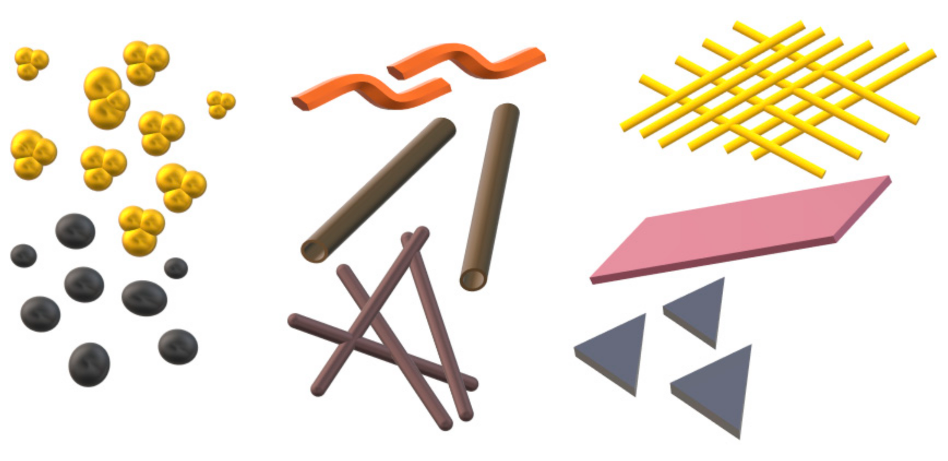
Figure 2.
Number of papers on one-dimensional nanostructures in 2000–2021 (keywords: nanotubes, nanofibers, nanowires, Scopus database).
Figure 2.
Number of papers on one-dimensional nanostructures in 2000–2021 (keywords: nanotubes, nanofibers, nanowires, Scopus database).
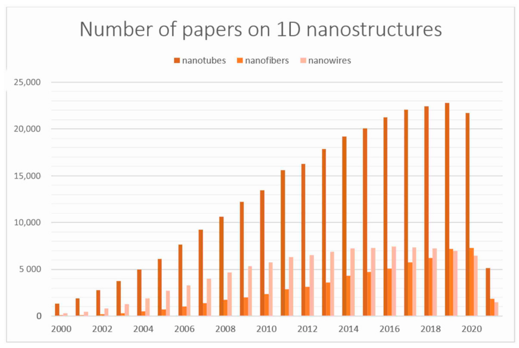
Figure 3.
Electrospinning devices used in the laboratory of the Department of Engineering Materials and Biomaterials at the Silesian University of Technology.
Figure 3.
Electrospinning devices used in the laboratory of the Department of Engineering Materials and Biomaterials at the Silesian University of Technology.
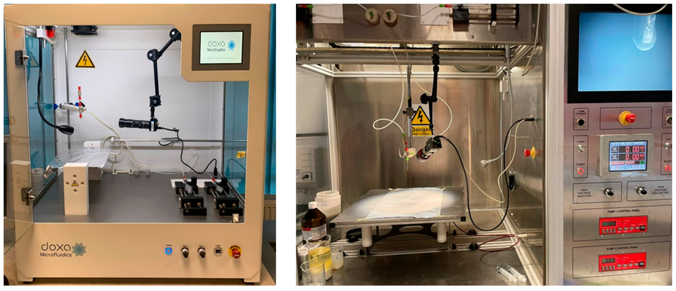
Figure 4.
Diagram of electrospinning process parameters.
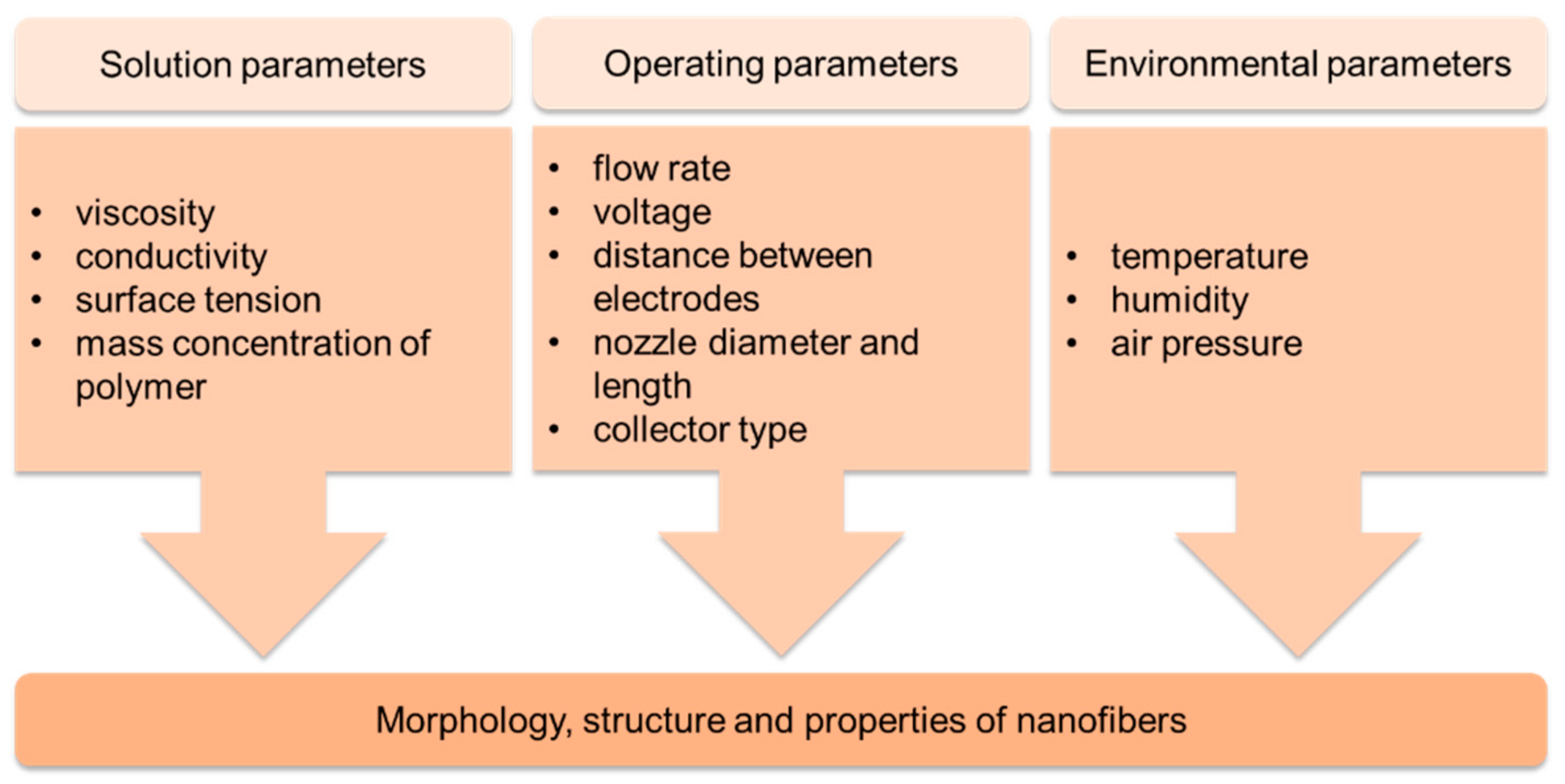
Figure 5.
Scheme of metal oxide nanowires formation in 3 main stages: solution preparation, electrospinning and calcination process.
Figure 5.
Scheme of metal oxide nanowires formation in 3 main stages: solution preparation, electrospinning and calcination process.
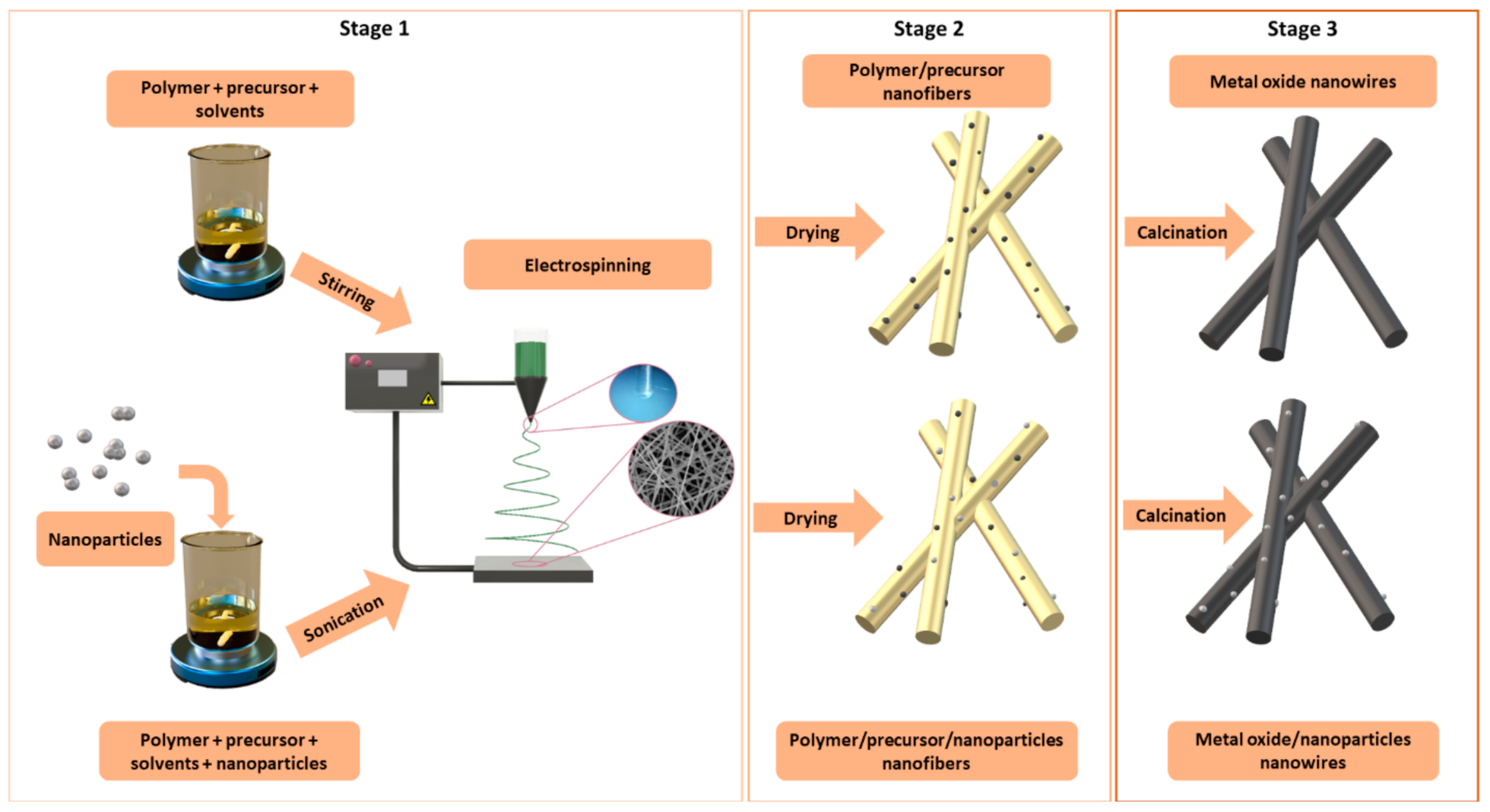
Figure 6.
Scanning Electron Microscope (SEM) images of (a) PVP/SnCl4 nanofibers, (b) PVP/In(NO3)3 nanofibers (Stage 2 Figure 5. (c,e) SnO2 nanowires after calcination in 500 °C, (d,f) In2O3 nanowires after calcination in 500 °C (Stage 3 Figure 5), Transmission Electron Microscope (TEM) images of (g) SnO2, (h) In2O3 single nanowire, Selected Area Electron Diffraction (SAED) patterns of: (i) SnO2 nanowires and (j) In2O3 nanowires [own study].
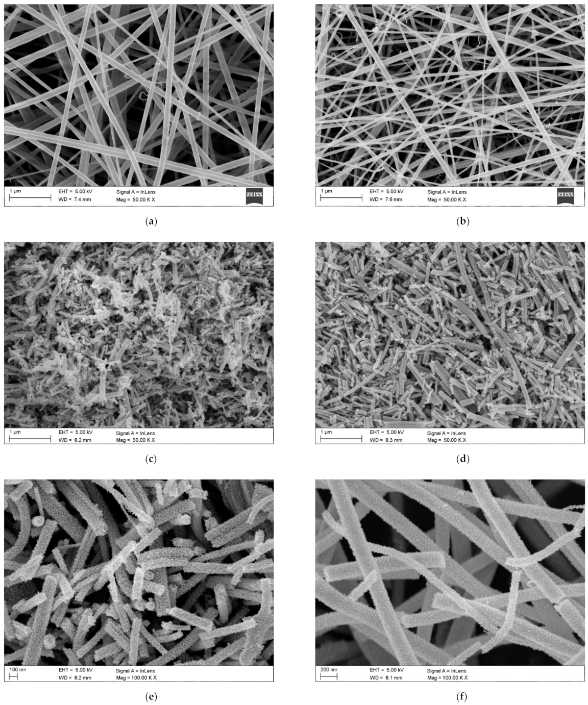
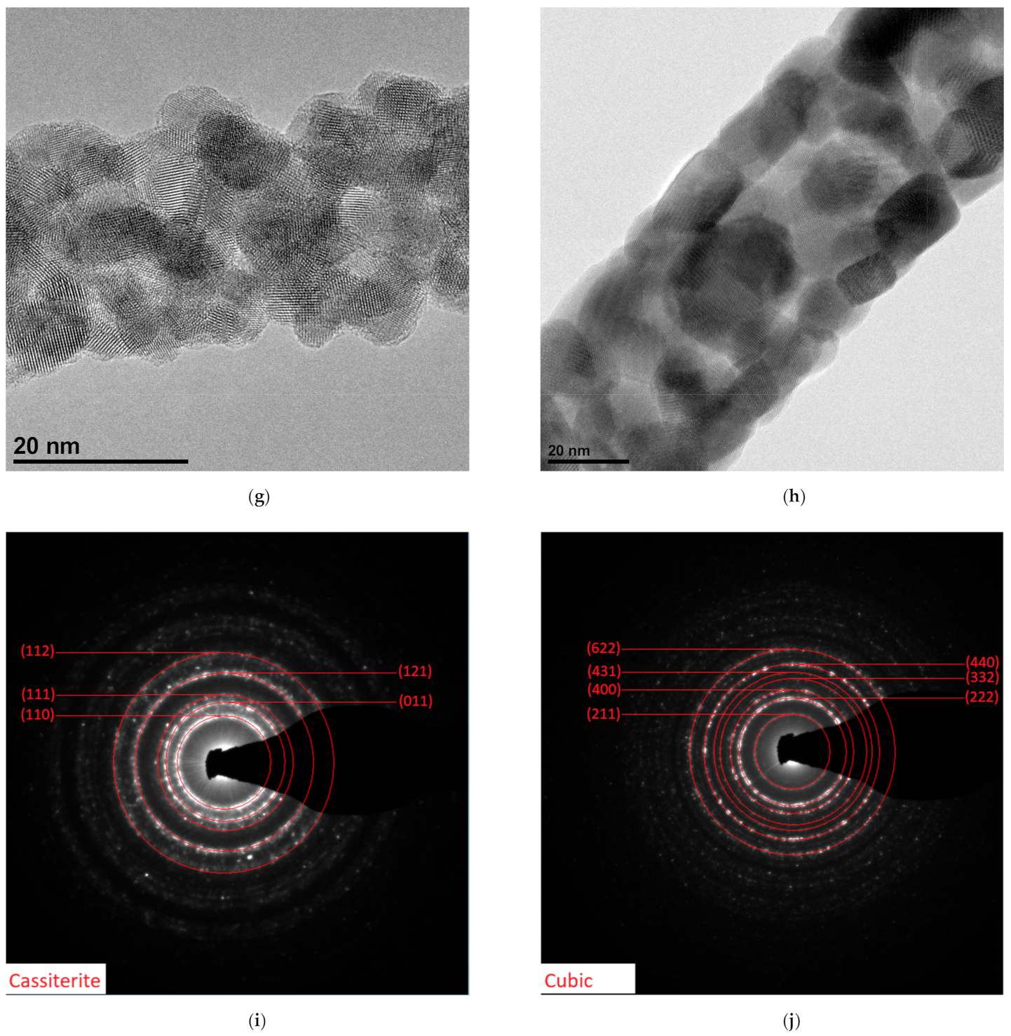
Figure 7.
Various 1D morphologies of SnO2 nanostructures produced by electrospinning: (a) traditional nanowires; (b) nanowires decorated with nanoparticles; (c) nanotubes [own study].
Figure 7.
Various 1D morphologies of SnO2 nanostructures produced by electrospinning: (a) traditional nanowires; (b) nanowires decorated with nanoparticles; (c) nanotubes [own study].
Figure 8.
Research methodology of nanomaterials produced by the electrospinning method.
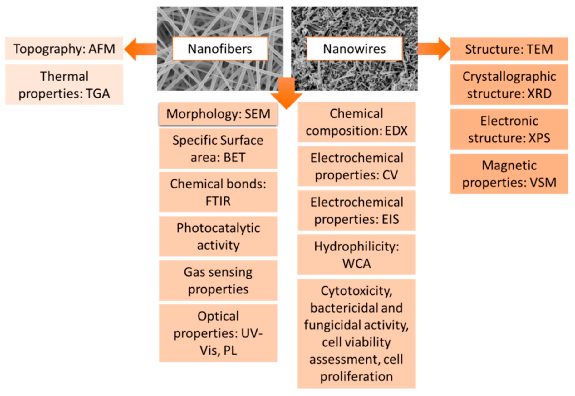
Figure 9.
SEM image of surface morphology of (a) TiO2 nanowires after calcination at 400 °C, (b) ZnO nanowires after calcination at 400 °C [own study].
Figure 9.
SEM image of surface morphology of (a) TiO2 nanowires after calcination at 400 °C, (b) ZnO nanowires after calcination at 400 °C [own study].
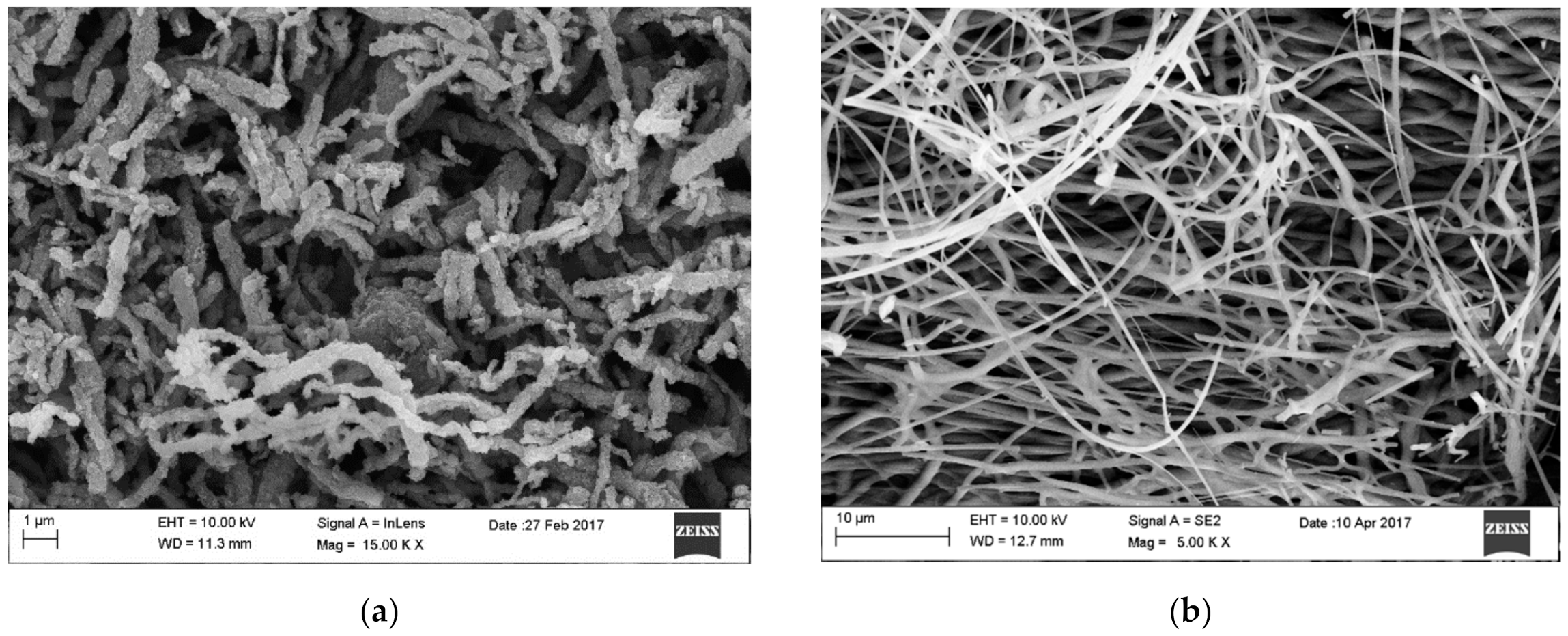
Figure 10.
Diagram of the photocatalytic activation of nanotubes SnO2 [113].
Figure 10.
Diagram of the photocatalytic activation of nanotubes SnO2 [113].
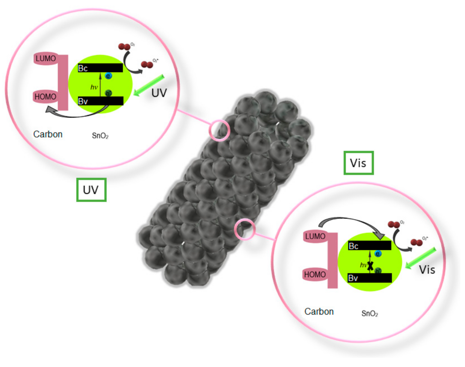
Figure 11.
(a) SEM image of SnO2 nanowires calcined in 500 °C (Reprinted with kind permission from Springer [24]); UV-VIS: (b) absorption spectrum of SnO2 nanowires calcined in 500 °C (Reprinted with kind permission from Nature [126]).
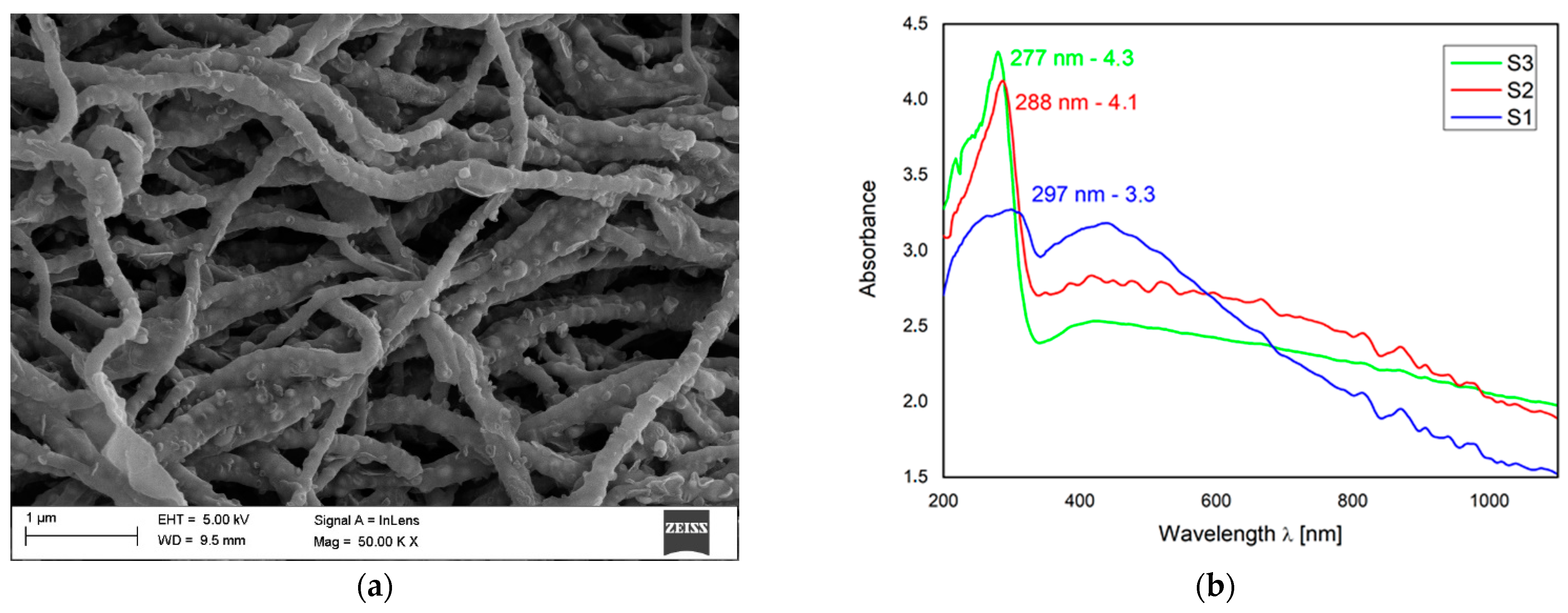
Figure 12.
Schematic representation of multilayer flexible photovoltaic architecture manufactured in Department of Engineering Materials and Biomaterials [Poster at the 5th China (Shanghai) International Invention & Innovation Expo: “Innovative flexible solid-state solar cell with a hybrid layered architecture”].
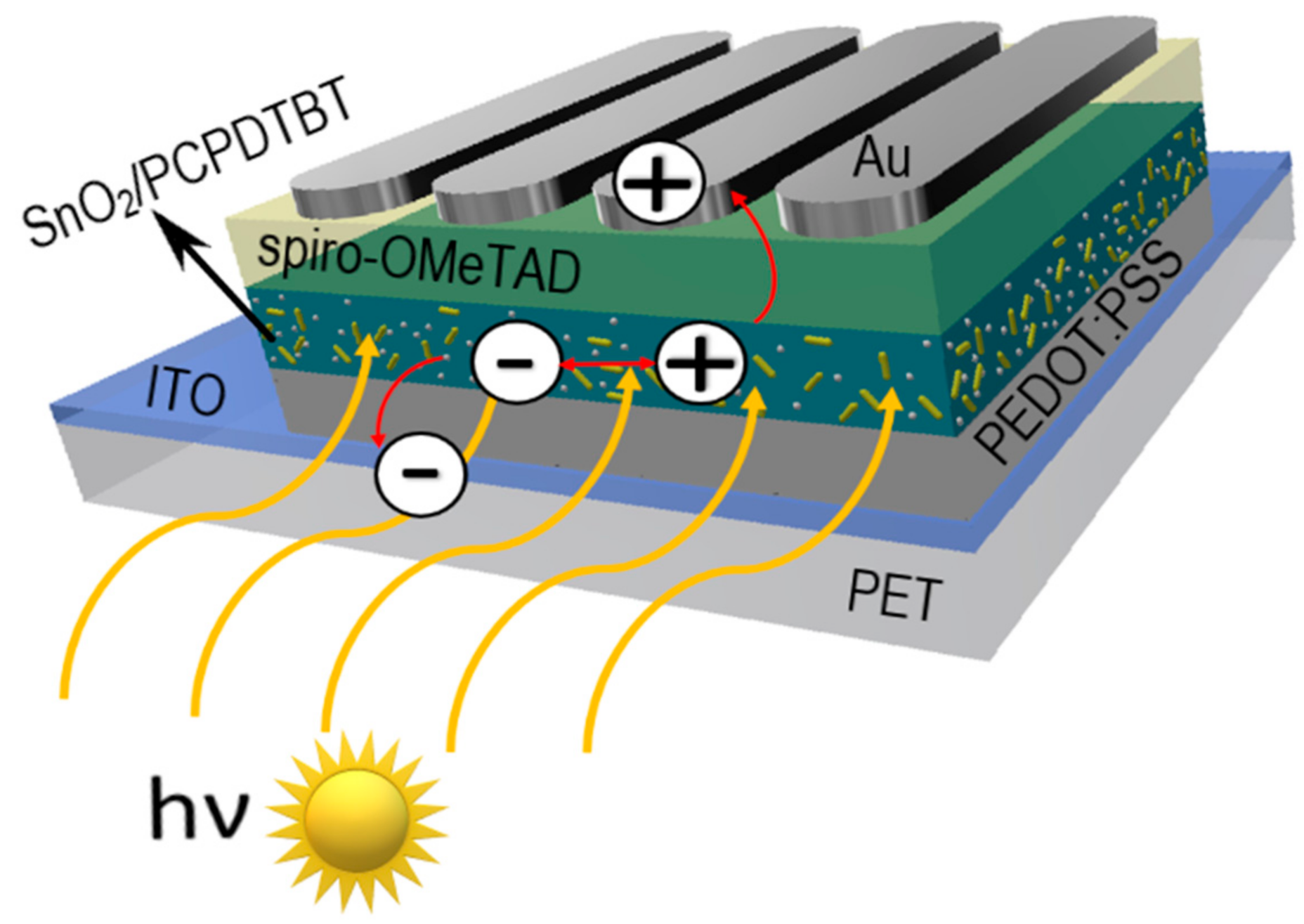
Figure 13.
Types of morphology of the most commonly produced 1D nanostructures.
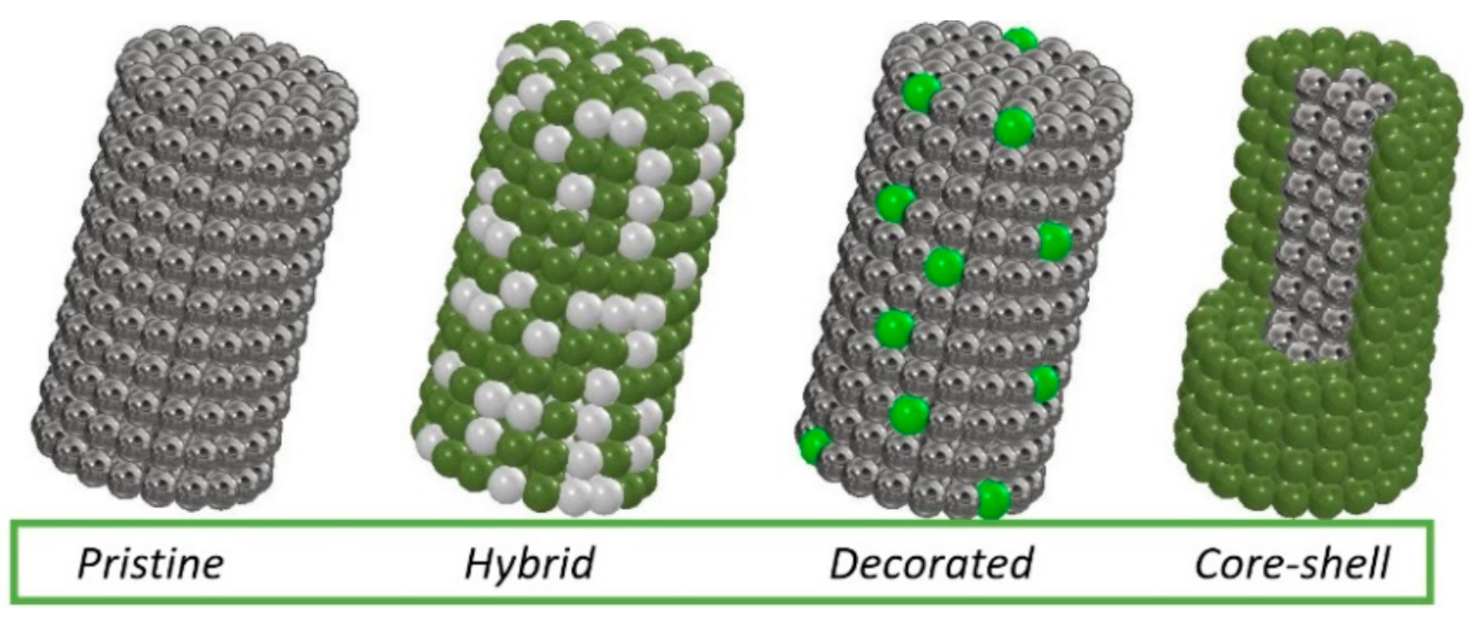
Figure 14.
Scheme of hollow structure of gas adsorption and depletion layer for ZnO-SnO2 composite [143].
Figure 14.
Scheme of hollow structure of gas adsorption and depletion layer for ZnO-SnO2 composite [143].
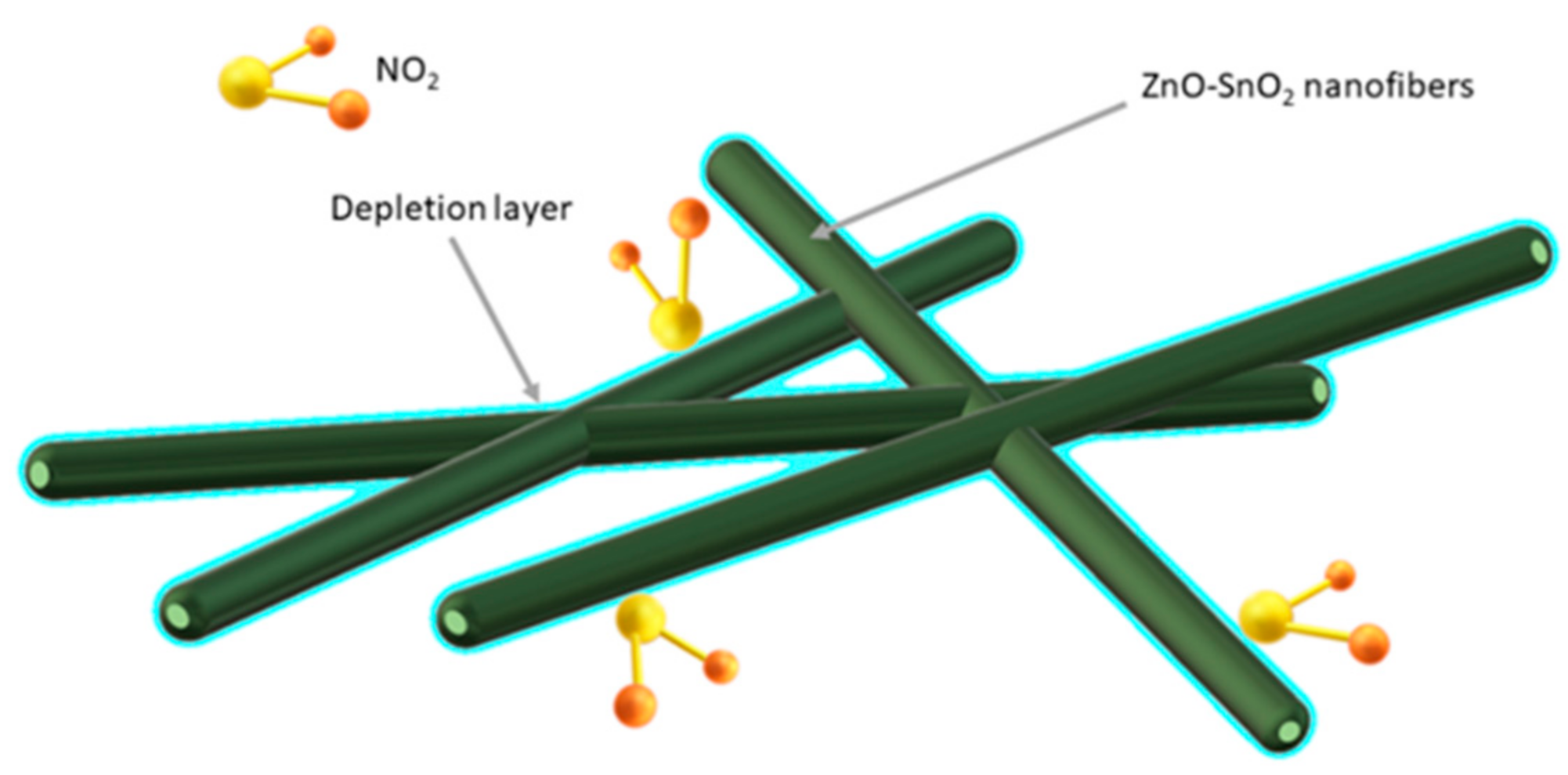
Figure 16.
Scheme of the manufacturing process of C/SnO2 nanofibers with a different morphology.
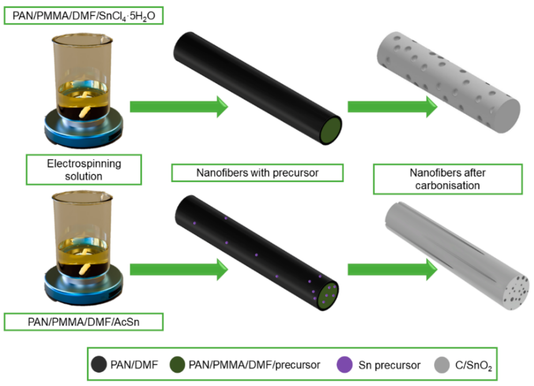
Table 2.
Selected popular 1D metal oxides with examples of reagents used for their fabrication.
| Material | Polymer | Precursor | Calcination Temperature | Ref. |
|---|---|---|---|---|
| TiO2 | PVP | Ti(OCH(CH3)2)4 | 450 | [85] |
| TiO2 | PVP | C16H36O4Ti | 500 | [86] |
| ZnO | PVA | Zn(CH3CO2)2·2H2O | 400/500/600 | [65] * |
| ZnO | PVP | Zn(CH3CO2)2·2H2O | 350–600 | [87] |
| SiO2 | PVP | Si(OC2H5)4 | 600 | [22] |
| SiO2 | PVA | Si(OC2H5)4 | 600 | [88] |
| WO3 | PVA | (NH4)6H2W12O40H2O | 400/500/600/700 | [89] |
| WO3 | PVP | WCl6 | 450–600 | [90] |
| CuO | PVP | Cu(CH3COO)2 | 500/600/700/800/900/1000 | [91] * |
| CuO | PVP | Cu(NO3)2∙3H2O | - | [92] |
| Fe2O3 | PVA | Fe(NO3)3·9H2O | 800 | [93] |
| Fe2O3 | PVP | Fe(CH3COO)2 | 500/600/700/800/900/1000 | [94]* |
| SnO2 | PVA | SnCl2·2H2O | 300/500/700 | [95] |
| SnO2 | PVP | SnCl2·2H2O | 500/600 | In press * |
| Bi2O3 | PAN | Bi(NO3)3 | 500/550/600 | [96] |
| Bi2O3 | PVP | Bi (NO3)3.5H2O | 450 | [97] |
| In2O3 | PVP | In(NO3)3·4.5H2O | 600 | [18] |
| In2O3 | PVP | In(NO3)3·xH2O | 600 | [98] |
* Polish scientific units.
Table 3.
Optical properties of selected 1D metal oxides prepared via electrospinning.
| MOS | TiO2 | ZnO | SiO2 | SnO2 | Bi2O3 | In2O3 |
|---|---|---|---|---|---|---|
| Direct band gap [eV] | 2.91–2.94 | 3.32–3.36 | 3.93–3.97 | 3.30–3.58 | 2.48–2.72 | 2.92–3.34 |
| Ref. | [86] | [65] | [11] | [108] | [109] | [23,110] |
Table 4.
Optical properties of TiO2 nanowires and ZnO nanowires after calcination at 400 °C [own study].
Table 4.
Optical properties of TiO2 nanowires and ZnO nanowires after calcination at 400 °C [own study].
| Material | Calcination Temperature [°C] | Max. Absorbance | Wavelength [nm] | Eg [eV] |
|---|---|---|---|---|
| TiO2 nanowires | 400 | 2.42 | 248 | 3.73 |
| 500 | 2.34 | 3.83 | ||
| 600 | 2.26 | 3.88 | ||
| ZnO nanowires | 400 | 2.94 | 346 | 3.36 |
| 500 | 3.38 | 3.34 | ||
| 600 | 3.43 | 3.32 |
Table 5.
Refractive index and dielectric permittivity obtained for the electrospun 1D SnO2 nanomaterials [24].
Table 5.
Refractive index and dielectric permittivity obtained for the electrospun 1D SnO2 nanomaterials [24].
| Parameter | SnO2 Nanowires | ||
|---|---|---|---|
| Type of Spinning Solutions | |||
| Type 1 | Type 2 | Type 1 | |
| refractive index (n) | 1.51 | 1.52 | 1.51 |
| complex dielectric permeability (ε) | 2.28 | 2.30 | 2.28 |
| Energy band gap (Eg) | 3.3 | 3.8 | 3.9 |
Publisher’s Note: MDPI stays neutral with regard to jurisdictional claims in published maps and institutional affiliations. |
© 2021 by the authors. Licensee MDPI, Basel, Switzerland. This article is an open access article distributed under the terms and conditions of the Creative Commons Attribution (CC BY) license (https://creativecommons.org/licenses/by/4.0/).
Share and Cite
MDPI and ACS Style
Smok, W.; Tański, T. A Short Review on Various Engineering Applications of Electrospun One-Dimensional Metal Oxides. Materials 2021, 14, 5139. https://doi.org/10.3390/ma14185139
AMA Style
Smok W, Tański T. A Short Review on Various Engineering Applications of Electrospun One-Dimensional Metal Oxides. Materials. 2021; 14(18):5139. https://doi.org/10.3390/ma14185139
Chicago/Turabian StyleSmok, Weronika, and Tomasz Tański. 2021. "A Short Review on Various Engineering Applications of Electrospun One-Dimensional Metal Oxides" Materials 14, no. 18: 5139. https://doi.org/10.3390/ma14185139
Note that from the first issue of 2016, this journal uses article numbers instead of page numbers. See further details here.