Review

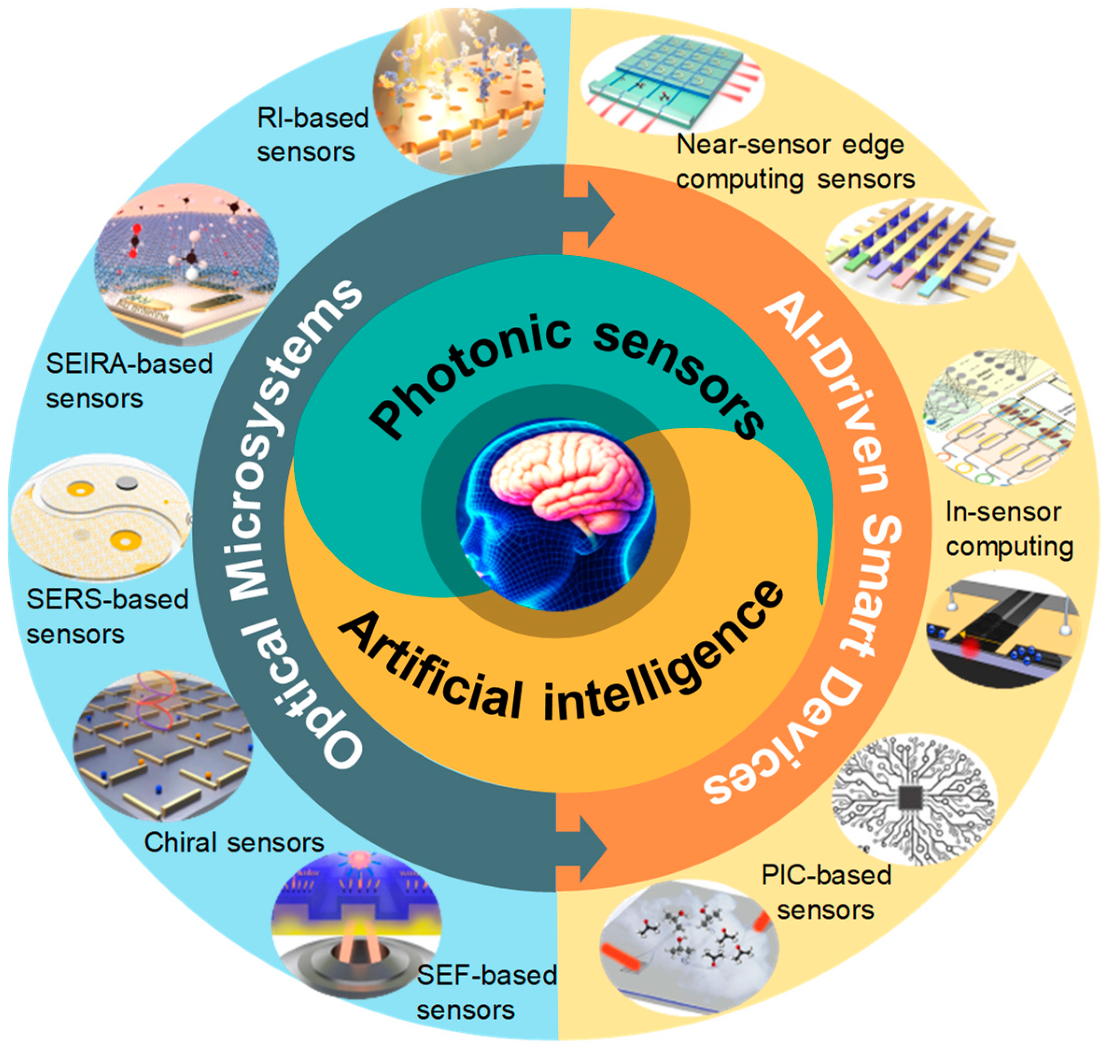
Technology Landscape Review of In-Sensor Photonic Intelligence: From Optical Sensors to Smart Devices

by
Hong Zhou
1,*,
Dongxiao Li
2 and
Chengkuo Lee
2,*
1
Ministry of Education Key Laboratory of Micro and Nano Systems for Aerospace, School of Mechanical Engineering, Northwestern Polytechnical University, Xi’an 710072, China 2 Department of Electrical and Computer Engineering, National University of Singapore, Singapore 117583, Singapore
2
Department of Electrical and Computer Engineering, National University of Singapore, Singapore 117583, Singapore
*
Authors to whom correspondence should be addressed.
AI Sens. 2025, 1(1), 5; https://doi.org/10.3390/aisens1010005
Submission received: 1 June 2025 / Revised: 5 July 2025 / Accepted: 9 July 2025 / Published: 14 July 2025

Abstract

Optical sensors have undergone significant evolution, transitioning from discrete optical microsystems toward sophisticated photonic integrated circuits (PICs) that leverage artificial intelligence (AI) for enhanced functionality. This review systematically explores the integration of optical sensing technologies with AI, charting the advancement from conventional optical microsystems to AI-driven smart devices. First, we examine classical optical sensing methodologies, including refractive index sensing, surface-enhanced infrared absorption (SEIRA), surface-enhanced Raman spectroscopy (SERS), surface plasmon-enhanced chiral spectroscopy, and surface-enhanced fluorescence (SEF) spectroscopy, highlighting their principles, capabilities, and limitations. Subsequently, we analyze the architecture of PIC-based sensing platforms, emphasizing their miniaturization, scalability, and real-time detection performance. This review then introduces the emerging paradigm of in-sensor computing, where AI algorithms are integrated directly within photonic devices, enabling real-time data processing, decision making, and enhanced system autonomy. Finally, we offer a comprehensive outlook on current technological challenges and future research directions, addressing integration complexity, material compatibility, and data processing bottlenecks. This review provides timely insights into the transformative potential of AI-enhanced PIC sensors, setting the stage for future innovations in autonomous, intelligent sensing applications.

1. Introduction

Optical sensing technologies have undergone a dramatic evolution from early discrete microsystems to today’s highly integrated smart photonic platforms [1]. Traditional optical sensors often required standalone components (lasers, lenses, detectors) assembled in bench-top or micro-optical setups, which limited their portability and scalability. While traditional discrete optical sensing systems typically exhibited high sensitivity due to individually optimized components, they also suffered from high power consumption, bulky configurations, complex alignment processes, and limited portability [2]. The advent of photonic integrated circuits (PICs) has enabled the miniaturization of these optical systems onto millimeter-scale chips [3], drastically reducing size, weight, and alignment complexity. By amalgamating light sources, waveguides, modulators, and photodetectors on a single chip [4,5], PIC-based sensors can be more compact, energy-efficient, and cost-effective than their bulk optical predecessors. This integration is especially crucial for portable and wearable applications, where size and power are at a premium [6].
At the same time, artificial intelligence (AI) has begun to play a transformative role in sensing [7,8,9,10,11]: machine learning algorithms are now routinely used to enhance signal processing, perform pattern recognition on complex optical spectra, and even control sensor operations in real time. AI-driven intelligent sensing provides several core advantages, including enhanced sensitivity and accuracy, real-time decision-making capabilities, and improved robustness and adaptability [12,13,14,15]. Machine learning algorithms enhance accuracy by effectively extracting subtle features from complex optical spectra, significantly surpassing conventional methods. Additionally, AI integration enables real-time, edge-level decision making, thus reducing latency and eliminating dependence on cloud computing, crucial for time-sensitive applications such as medical diagnostics and autonomous vehicles. Marrying PIC technology with AI-driven data analysis has given rise to a new class of smart photonic sensors that can not only detect environmental or biochemical signals but also interpret and respond to them autonomously [16]. For example, modern point-of-care diagnostic devices have combined nanophotonic sensor chips with AI-based spectral pattern recognition to identify pathogens within minutes [17]—a task that previously required lengthy laboratory analysis. Edge intelligence is emerging [18], whereby intensive computations are performed locally at the sensor, enabling immediate decision making without reliance on cloud computing. This trend toward on-chip intelligence is accelerating the development of photonic integrated circuit sensors that are AI-driven smart devices, capable of real-time sensing and interpretation.
In the following sections, we review the landscape of optical sensor technology leading up to this convergence (Figure 1). We first overview conventional optical sensing techniques—from refractive index (RI) sensing, surface-enhanced infrared absorption (SEIRA) spectroscopy, surface-enhanced Raman spectroscopy (SERS) and surface plasmon-enhanced chiral spectroscopy to surface enhanced fluorescence (SEF) spectroscopy—which laid the groundwork for current systems. We then discuss representative applications of optical sensors in healthcare, environmental monitoring, and chemical detection. Next, we describe the architecture of photonic integrated circuits and introduce the concept of in-sensor computing, where computational tasks are embedded within the sensor hardware. Finally, we examine current research frontiers and challenges and provide an outlook on the future trajectory toward fully autonomous, miniaturized, and intelligent photonic sensing systems.

2. Basic Sensing Technologies

Before the era of PICs, a rich variety of optical sensing methodologies were developed in free-space or fiber-optic formats [19,20,21]. These conventional optical sensors exploited different light–matter interaction mechanisms to detect physical, chemical, or biological quantities. Here, we provide a brief overview of several important techniques: RI-based sensors, SEIRA-based sensors, SERS-based sensors, chiral sensors, and SEF-based sensors. Each of these approaches has distinct principles and strengths, and they continue to inform the design of integrated photonic sensors.

2.1. Mechanism of RI Sensing

Surface plasmons offer an exceptionally sensitive route to refractive-index (RI) sensing by confining the electromagnetic field at the metal–dielectric interface [22,23,24]. Plasmon-based RI sensors combine several attractive features: high sensitivity (Figure 2a) [25,26], calibration-free operation, real-time monitoring, and noninvasive, label-free detection. By functionalizing the sensor surface with a thin film of biorecognition elements—for instance, antibodies, aptamers, or molecular imprints—one can selectively capture target analytes from biological, chemical, or gaseous samples. Upon binding, these targets alter the local RI near the plasmonic surface, which in turn shifts the resonance wavelength, amplitude, or phase of the plasmonic mode [27]. Tracking these signal variations provides kinetic information on molecular interactions, allowing for quantitative analysis of specificity, binding affinity, and reaction dynamics. Two key figures of merit govern plasmonic RI sensor performance: the RI sensitivity (SRI) and the sensor’s figure of merit (FoM). Sensitivity is defined as [28]
S R I = Δ λ Δ n
where Δn is the change in refractive index and Δλ is the corresponding shift in resonance wavelength. The FoM normalizes this sensitivity by the resonance linewidth, typically expressed as the full width at half maximum (FWHM), and is given by [29]
F o M = S R I F W H M
Higher values of SRI and FoM both indicate superior sensor performance, reflecting greater wavelength shifts per RI unit and sharper resonance features for more precise detection.

2.2. Sensing Mechanism of Surface-Enhanced Infrared Absorption (SEIRA) Spectroscopy

Infrared spectroscopy offers a uniquely powerful window into biochemical systems by capturing the distinct vibrational “fingerprints” of their molecular constituents [30,31,32]. Its intrinsic chemical specificity, coupled with label-free, noninvasive, real-time measurement capabilities, has driven breakthroughs in fields ranging from environmental surveillance and defense to chemical analysis and medical diagnostics. Yet traditional infrared methods suffer from inherently low sensitivity when probing molecules whose absorption cross-sections are tiny compared to the micron-scale wavelengths of IR light [33,34,35].
Plasmonic nanoantennas remedy this mismatch by funneling and concentrating incident radiation into nanoscale “hot spots,” where the local electromagnetic field is dramatically intensified. This strong light–matter coupling enables the detection of otherwise-weak vibrational features, a phenomenon known as surface-enhanced infrared absorption (SEIRA) spectroscopy (Figure 2b) [7]. The standard figure of merit for SEIRA performance is the enhancement factor (EF), defined as
E F = I S E I R A I r e f N r e f N S E I R A
where ISEIRA is the vibrational absorption intensity after plasmonic coupling, Iref is the corresponding intensity for an uncoupled (pure) molecular sample, NSEIRA denotes the number of molecules located within the antenna’s electromagnetic hot spots, and Nref is the total number of molecules in the reference measurement. This metric, thus, captures both the optical “gain” provided by the antenna and the fraction of molecules experiencing that enhancement.

2.3. Sensing Mechanism of Surface-Enhanced Raman Spectroscopy (SERS)

Raman spectroscopy probes the vibrational and rotational modes of molecules and crystal lattices through inelastic scattering [36,37,38]. When a sample is illuminated with a laser or other monochromatic light, its molecules vibrate and scatter photons at shifted frequencies. By measuring the frequency shifts and intensities of this scattered light, Raman spectroscopy reveals detailed information about molecular structure and bonding. However, because spontaneous Raman scattering is inherently weak and often overwhelmed by much stronger Rayleigh (elastic) scattering, its sensitivity is limited.
Surface-enhanced Raman scattering (SERS) overcomes this drawback by amplifying the Raman signal by several orders of magnitude (Figure 2c) [39,40,41]. In SERS, metal nanostructures—typically silver or gold nanoparticles—serve as “hot spots” that concentrate and enhance the local electromagnetic field (electromagnetic enhancement) and facilitate charge transfer between the substrate and adsorbed molecules (chemical enhancement). A SERS substrate is created by depositing these nanoparticles onto a surface, dramatically boosting the intensity of the scattered light. The calculation formula for SERS intensity is
I S E R S I 0 E ω e x t E ω d e t E 0 ω e x t E 0 ω d e t 2
Among them, the enhancement factor (EF) scales with the square of the ratio between the enhanced local field strength (E) and the incident field strength (E0), evaluated at both the excitation frequency (ωext) and the Raman detection frequency (ωdet). Thanks to its ultra-high sensitivity and molecular selectivity, SERS has rapidly become a powerful tool for detecting trace analytes. Advances in SERS theory, substrate engineering, and instrumentation have expanded its applications across biomedical diagnostics, nanomaterial characterization, food safety testing, and environmental monitoring.

2.4. Sensing Mechanism of Surface Plasmon-Enhanced Chiral Spectroscopy

Chiral molecules are those whose structures cannot be superimposed on their mirror images by any combination of rotations or translations (Figure 2d) [42,43,44]. As a result, each chiral compound exists as two distinct, non-overlapping forms called enantiomers. Chirality is a fundamental characteristic found throughout nature, particularly in biomolecules; for instance, amino acids and nucleic acids each occur as left- and right-handed versions. Although both enantiomers share identical elemental composition and functional groups, their chemical behaviors can differ dramatically. This distinction is especially critical in pharmaceuticals and agrochemicals, where one enantiomer may be therapeutically active while its counterpart is inert or even harmful. Consequently, the ability to detect and differentiate between enantiomers is essential across analytical chemistry, biomedicine, drug manufacturing, and toxicology. Traditional techniques such as optical rotatory dispersion (ORD) and circular dichroism (CD) spectroscopy are routinely employed to probe molecular chirality. However, because the helical pitch of many chiral molecules is much smaller than the wavelength of visible light, these conventional methods often struggle to capture chiral signals from minute sample volumes. Recent breakthroughs in nanophotonics offer promising solutions; for example, engineered metasurfaces with chiral architectures can generate areas of intense optical chirality and boost CD responses, thereby amplifying otherwise-weak chiral signatures.

2.5. Sensing Mechanism of Surface-Enhanced Fluorescence (SEF) Spectroscopy

Fluorescence detection is a cornerstone of life-science research and medical diagnostics because it offers exceptionally low detection limits and a wide variety of fluorophores, enabling the simultaneous monitoring of multiple biomarkers [45,46,47]. However, at low analyte concentrations, the emitted fluorescence can become exceedingly weak, necessitating sophisticated, costly, and often bulky equipment to preserve high sensitivity. Such large instruments are impractical for disease diagnosis in resource-constrained environments. In recent years, plasmonic nanostructures composed of noble metals have emerged as an elegant strategy to amplify fluorophore signals without complex hardware. When illuminated, metal nanoparticles support localized surface plasmon resonances at their metal–dielectric boundaries, intensifying the nearby electromagnetic field and boosting the fluorophore’s excitation rate. Simultaneously, an elevated local density of optical states enhances the fluorophore’s emission probability, shortening its fluorescence lifetime and raising its quantum yield. By positioning fluorophores in close proximity to conductive metal surfaces or particles, one harnesses this surface-enhanced fluorescence (SEF) phenomenon (Figure 2e) to achieve much stronger signals with simpler, more compact platforms.

3. Applications of Optical Sensors

3.1. Refractive Index Sensing

Plasmonic refractive-index sensors have become invaluable tools in biological research and clinical diagnostics owing to their simplicity and affordability. Unlike conventional methods such as enzyme-linked immunosorbent assays (ELISA) or polymerase chain reaction (PCR), plasmonic RI sensors enable noninvasive, real-time, label-free, and rapid biomarker quantification. A prominent example is the detection of the prostate-specific antigen (PSA), a key indicator used in prostate cancer screening [48]. In healthy individuals, PSA levels typically range from 4.0 to 10 ng/mL [49], while concentrations exceeding 10 ng/mL signal an elevated cancer risk. Early and accurate PSA measurement is, therefore, critical. In 2018, Khan et al. designed a gold nanodisc array functionalized with PSA-specific DNA aptamers (Figure 3a) [50]. By tuning the nanodisc dimensions, they achieved a localized plasmon resonance at 646 nm. This aptamer-modified platform delivered a sensitivity of 113 nm/RIU, a detection limit as low as 1.49 ng/mL, and a dynamic range spanning 1.7–20.4 ng/mL. Furthermore, through a self-assembly process, PDMS/Pd–WO3 and a microbottle resonator can develop a simple, low-cost fiber-optic hydrogen sensor that achieves a maximum sensitivity of –3.091 nm/%H2 at 25 °C with minimal interference from humidity or temperature changes [51].
Beyond protein markers, plasmonic RI sensors can also target tumor-derived exosomes, 50–150 nm extracellular vesicles present in bodily fluids such as blood, urine, and saliva [52,53,54,55,56], that mediate intercellular communication by ferrying molecular cargo [57,58,59]. Elevated exosome levels have been correlated with malignancy, making them promising diagnostic biomarkers. However, traditional exosome assays often demand extensive sample purification and labeling, hindering device miniaturization and point-of-care deployment [60]. To overcome these challenges, Lm et al. introduced the nanoplasmonic exosome (nPLEX) assay [61], which employs periodic nanohole arrays to induce strong surface plasmon resonances. Exosome binding shifts the resonance signal, and quantitative analysis is performed by monitoring phase or intensity changes; matching the array periodicity to exosome size further enhances sensitivity. Building on this, Lim and colleagues later developed the amplified plasmonic exosome (APEX) platform (Figure 3b) [62], which uses localized optical deposition and in situ enzymatic transformation on bilayer plasmonic nanostructures for multiplexed exosome profiling. This approach achieves a sensitivity of approximately 200 exosomes and can distinguish between exosome-bound and unbound amyloid β populations directly in blood, offering a minimally invasive means to assess cerebral plaque burden in Alzheimer’s disease.
The COVID-19 pandemic has underscored the urgent need for rapid, reliable diagnostics [63], particularly in resource-limited settings where shortages of medical infrastructure can hinder containment efforts and increase morbidity and mortality among vulnerable populations [64,65]. Although numerous antigen- and antibody-based assays have been developed for SARS-CoV-2 detection [66,67], plasmonic RI sensors stand out for their label-free, real-time operation [68,69,70,71]. For instance, Funari and colleagues engineered a gold-nanospike optofluidic platform that exploits localized surface plasmon resonance (LSPR) to detect anti-spike protein antibodies in plasmon [72]. Antigen–antibody binding alters the local refractive index around the nanospikes, producing a measurable red shift in the LSPR peak; this system achieves a sensitivity of 183 nm/RIU and a detection limit of 0.5 pM [73,74,75]. Similar plasmonic RI approaches have since been applied to the detection of other viral targets, demonstrating the broad applicability of this technology. In addition, Grosman et al. (2023) reported a chip-scale photonic sensor comprising two silicon-nitride microring resonators—one functionalized with SARS-CoV-2 DNA primers and the other serving as a reference [76]. The platform achieves label-free detection of viral RNA at concentrations as low as 10 cp/μL, with a sensitivity of 750 nm/RIU, and operates robustly under varying environmental conditions.
Despite their sensitivity, conventional plasmonic setups often rely on high-performance spectrometers that are bulky, costly, and complex—obstacles to widespread adoption in point-of-care and field settings. To address these limitations [77,78], researchers have developed spatial-multiplexing metasurfaces that encode refractive-index changes as variations in far-field intensity patterns. By illuminating a gradient or pixelated metasurface with narrowband light and capturing its position-dependent scattering with a simple camera [79], one can monitor analyte binding events through real-time intensity shifts, obviating the need for precision spectrometers [80,81,82]. This strategy has yielded remarkably sensitive and streamlined sensing platforms. For example, Ansaryan et al. introduced a label-free nanoplasmonic imaging system that maps single-cell secretions in a microwell array (Figure 3c) [83]: gold nanohole arrays support the plasmon resonances, and a complementary metal-oxide camera records intensity changes driven by molecular attachment. Coupled with machine-learning–based image analysis, this approach enables high-throughput, spatiotemporal monitoring of hundreds of individual cells, paving the way for parallelized, real-time molecular diagnostics.
Optical fibers have emerged as a powerful platform for biosensing in early medical diagnostics due to their low cost, mechanical flexibility, compact form factor, immunity to electromagnetic interference, and suitability for remote monitoring. However, their inherently modest sensitivity has posed a major challenge for detecting low-abundance biomarkers. To address this, researchers have harnessed localized surface plasmon resonance (LSPR) in metallic nanostructures to amplify the evanescent field at the fiber surface, markedly boosting sensor performance.
Building on these advances, plasmonic optical microfiber biosensors have been shown to detect individual biomolecules and nanoparticles ranging from roughly 50 to 500 nm in diameter [84,85,86,87,88]. In a notable extension of this concept, Huang and colleagues engineered a dual-amplification interface that couples plasmonic enhancement with an aptamer-driven conformational switch (Figure 3d). This design enables single-molecule sensing of small targets such as dopamine in complex biological fluids [89], achieving detection limits down to approximately 1.3 attomolar in cerebrospinal fluid, 1.5 attomolar in whole serum, and 0.5 attomolar in artificial sweat. By simply exchanging the aptamer sequence, the same platform can be adapted to sense a wide variety of other small molecules and ions at the single-molecule level [90,91,92,93].
In recent years, significant progress has been made in waveguide-based RI sensors [94,95]. Optical waveguides are dielectric structures that confine and guide light by means of total internal reflection or mode confinement in a high-refractive-index core surrounded by a lower-index cladding [96]. Waveguide-based RI sensors harness the evanescent field that extends beyond the waveguide core into the surrounding medium [97]. When the local refractive index changes, due to analyte binding, concentration shifts, or temperature variations, the effective index of the guided mode shifts accordingly. This perturbation can be detected by monitoring shifts in resonant wavelength, changes in transmitted intensity, or phase variations in interferometric setups.
Figure 3. RI-based sensing applications. (a) RI-based sensors for subtyping of circulating exosome-bound amyloid β reflects brain plaque deposition [50]. (b) RI-based sensors for label-free immunoassay boosting [62]. (c) RI-based sensors for high-throughput spatiotemporal monitoring of single-cell secretions [83]. (d) RI-based sensors for single-molecule and noninvasive dopamine detection [89]. (1) Loading dopamine molecules. (2) Binding of dopamine molecules to nanoparticles. (3) Frequency shift caused by combining.
Aisens 01 00005 g003

3.2. Surface-Enhanced Infrared Absorption Spectroscopy

Although refractive-index (RI) sensors offer user-friendly operation and high sensitivity, they are inherently limited by the fact that shifts in resonant frequency alone cannot reveal molecular identity, constraining their ability to distinguish between different analytes. Infrared absorption spectroscopy addresses this shortcoming by providing chemical-specific information via characteristic spectral fingerprints. Yet, the inherently low-absorption cross-section of most molecules renders conventional infrared techniques insufficiently sensitive for detecting trace concentrations [98,99]. Surface-enhanced infrared absorption (SEIRA) spectroscopy overcomes this barrier by exploiting plasmonic enhancement to amplify weak molecular signals [100,101,102]. First observed by Hartstein and colleagues in 1980 using randomly distributed metal island films [103], early SEIRA platforms suffered from non-resonant enhancement and modest field amplification (typically on the order of 101–102) [104,105]. The advent of engineered metasurfaces—with their precisely defined, periodic geometries—has revolutionized SEIRA [106,107,108,109,110], enabling higher and tunable resonance enhancement. Advances in micro- and nanofabrication have yielded a rich variety of metasurface motifs, including asymmetric crosses [111,112], split-ring resonators [113], and fractal architectures [114,115], each offering tailored control over electromagnetic fields to boost SEIRA performance. Nonetheless, these designs often remain constrained by human intuition, favoring simple two-dimensional geometries over potentially richer, multidimensional configurations [116].
Maximizing the spatial overlap between target molecules and the intense near-field “hot spots” around nanoantennas is equally crucial for SEIRA sensitivity. A significant portion of the enhanced field typically resides within the underlying dielectric substrate, limiting direct interaction with analyte molecules. To address this, researchers have developed nanopedestal platforms by etching away portions of the dielectric [117,118,119], thereby elevating the plasmonic elements into free space and increasing the overlap between molecules and hot spots. Compared to planar nanoantennas, these nanopedestals can deliver a 2.5–10-fold improvement in SEIRA sensitivity [118], further augmented by their passive ability to capture and concentrate analytes [120]. Alternatively, coating nanoantenna surfaces with molecule-enriching layers or functionalizing them with specific probe ligands has proven effective for the selective adsorption of proteins, nucleic acids, and lipids in liquid environments. Such chemical tailoring enables dynamic, real-time SEIRA detection of low-abundance biomolecules, broadening the technique’s applicability in biosensing and diagnostics (Figure 4a) [98,121,122,123,124,125,126].
Machine learning has accelerated advances in SEIRA spectroscopy (Figure 4b) [127,128,129]. For instance, Kavungal et al. combined an immunoassay with a nanoplasmonic infrared metasurface to selectively detect proteins implicated in neurodegenerative disorders [130]. By training an artificial neural network on the sensor’s spectral response, they achieved highly accurate quantification of complex mixtures containing both oligomeric and fibrillar aggregates. While SEIRA offers powerful insights into molecular dynamics, conventional infrared spectroscopy often struggles to disentangle overlapping vibrational bands. To address this, Zhou et al. engineered vertically stacked infrared nanoantennas that harness the hybridization between localized surface plasmons and surface phonon polaritons (SPhPs) [131]. Operating within the Reststrahlen band, these SPhPs exhibit extreme refractive-index sensitivity; when paired with deep learning algorithms, this platform can deconvolve strongly overlapping vibrational signatures arising during biological reactions.
In parallel, several strategies have emerged to push SEIRA sensitivity even further. The optimization of plasmonic loss profiles [132,133,134] and the synthesis of complex-frequency excitation waveforms [135] have both demonstrated appreciable gains in signal strength. Meanwhile, molecular enrichment coatings have proven highly effective for trace-gas detection [136,137,138,139,140]. For example, Zhou et al. applied a ZIF-8 film to capture and concentrate gas molecules on the sensor surface, yielding a significant boost in sensitivity (Figure 4c) [141]. Building on this approach, they subsequently employed MOF/polymer hybrid films to drive the CO2 detection limit down into the sub-parts-per-million regime [142].
Enhancing spectral bandwidth is another key objective in SEIRA, since broadband measurements capture richer molecular fingerprints for more precise identification and retrieval. To this end, a variety of metasurface architectures have been proposed to realize broadband or multiband plasmonic resonances, including fractal geometries [114,115,143], self-similar scaffolds [144,145], asymmetric resonators [111], gradient metasurfaces [146,147], and supercell designs [129]. A common approach is to co-locate nanoantennas tuned to different frequencies within a single unit cell [148]; however, as antenna density increases, so does inter-antenna coupling. Supercells—arrays of 16 hook-shaped nanoantenna sub-cells with gradually varying dimensions—effectively suppress this coupling and yield a continuous resonance spanning 6–9 μm (Figure 4d) [129]. Alternatively, stitching discrete resonances into a contiguous spectrum via spatial multiplexing establishes one-to-one mapping between the wavelength and position, enabling spectrometer-free detection [149,150,151,152], though at the expense of larger device footprints. To overcome this trade-off, Li et al. applied coupled-mode theory to design an overcoupled metamaterial absorber that delivers a uniform enhancement across 6–14 μm, allowing for the fingerprint retrieval of 13 analytes with a single metasurface array for the first time (Figure 4e) [128]. The broadband performance of such overcoupled resonators has since been further validated by Paggi et al. [153].
Figure 4. SEIRA-based sensing applications. (a) Multi-resonant SEIRA-based sensors for the detection of lipid membrane [104]. (b) SEIRA-based sensors for monitoring dynamics between all major classes of biomolecules [125]. (c) SEIRA-based sensors for simultaneous on-chip sensing of greenhouse gases [141]. (d) SEIRA-based sensors using wavelength-multiplexed hook nanoantennas [129]. (e) Ultrasensitive molecular fingerprint retrieval using strongly detuned overcoupled plasmonic nanoantennas [128].
Aisens 01 00005 g004

3.3. Surface-Enhanced Raman Spectroscopy

Raman spectroscopy serves as an invaluable complement to infrared absorption techniques. Although both probe molecular vibrations, infrared spectroscopy measures absorption while Raman relies on inelastic light scattering. Moreover, the strong absorption of mid-infrared light by water severely limits IR-based measurements in aqueous environments, whereas water’s inelastic Raman scattering cross-section is negligible. Consequently, Raman methods can capture vibrational fingerprints in high-water-content contexts, such as biological fluids or intracellular milieus, where infrared fails. Yet, the inherently weak Raman cross-sections of most molecules impede detection at low concentrations. SERS overcomes this limitation by exploiting plasmon-mediated electric-field amplification (and, in some cases, chemical enhancement) to boost Raman signals of trace analytes. First observed serendipitously by Fleischmann and colleagues, who noted the dramatically increased Raman intensity of pyridine on roughened silver electrodes, SERS has since evolved into a robust technique celebrated for its ultra-high sensitivity and molecular specificity, with applications spanning surface/interface chemistry, life sciences, clinical diagnostics, food safety, and environmental monitoring.
Surfaces and interfaces underpin critical phenomena in heterogeneous catalysis, electrochemistry, and photo (electro)chemistry, yet elucidating their molecular-scale behavior demands techniques with exceptional surface sensitivity. SERS excels in this regard. For example, Yu et al. introduced a depth-sensitive, plasma-enhanced Raman approach to probe both the nanostructure and chemical composition of the solid-electrolyte interphase (SEI) on lithium metal anodes (Figure 5a) [154]. Their dynamic, molecular-level insights into SEI formation and evolution offer a powerful guide for engineering more stable and higher-performance battery interfaces. Beyond energy storage, the combination of high spatial resolution and sub-nanometer hot spots in SERS substrates enables nanoscale chemical mapping and even single-molecule optomechanical studies.
The rich vibrational fingerprints accessible via SERS also pave the way for “photonic noses” and “photonic tongues”. Inspired by biological olfaction, Kim et al. fabricated an array of eight SERS substrates, each functionalized with a unique self-assembled monolayer, to create a receptor-agnostic sensing platform. By capturing multifaceted spectral signatures, this artificial-nose design achieves the high-accuracy discrimination of complex biological samples without relying on target-specific receptors. Similarly, Leong et al. developed a breathalyzer based on SERS for noninvasive COVID-19 screening, demonstrating 96.2% sensitivity and 99.9% specificity (Figure 5b) [155]. Extending SERS into liquid sensing, Ling and colleagues engineered a “SERS taster” for the multiplexed analysis of wine aromas (Figure 5c) [156]. By integrating multiple non-covalent receptor chemistries and constructing comprehensive “SERS superprofiles,” they achieved predictive flavor analytics via chemometric modeling. Together, these advances underscore SERS’s versatility in delivering molecular-level insights across both dry and liquid environments, and they highlight its central role in next-generation photonic sensing platforms.
The inherent rigidity of conventional SERS substrates poses a fundamental challenge for wearable applications on soft, dynamic biological surfaces. To bridge this mechanical mismatch, recent efforts have focused on engineering flexible, skin-conformable SERS platforms. For example, Wang et al. developed a stretchable plasmonic metasurface sensor that seamlessly integrates a flexible SERS-active metasurface with a compliant microfluidic system for continuous sweat sampling (Figure 5d) [157]. By harvesting analytes directly from epidermal sweat and exploiting each molecule’s unique Raman fingerprint, this device enables noninvasive, real-time molecular profiling. Building on this concept, Mogera et al. introduced a plasmonic-paper-based microfluidic wearable that concurrently quantifies sweat volume, rate, and metabolite concentrations (Figure 5e) [158]. Their integrated sensor achieves the sensitive detection of uric acid down to 1 μM in perspiration, demonstrating the promise of flexible SERS wearables for personalized health monitoring, point-of-care diagnostics, and responsive drug delivery systems.
Beyond human health, SERS has found emerging applications in plant physiology and agricultural management. Plants under biotic or abiotic stress secrete signaling metabolites, such as salicylic acid, extracellular ATP, phytoalexins, and glutathione, that govern defense pathways. Traditional assays often require destructive sampling, hindering real-time assessment. Addressing this, Son et al. introduced SERS nanoprobes into the plant apoplast to noninvasively track endogenous signaling molecules in situ (Figure 5f) [159]. Their approach successfully detected key stress markers in living nasturtium, wheat, and barley, providing dynamic insights into plant responses. Moreover, SERS platforms have been leveraged to monitor pesticide residues, illicit additives, and mycotoxins on harvested produce. Collectively, these advances highlight SERS’s versatility as a high-sensitivity, surface-specific tool for precision agriculture, where rapid, on-site analysis can optimize crop health, resource utilization, and yield quality.

3.4. Surface Plasmon-Enhanced Chiral Spectroscopy

Differentiating enantiomeric species is vital across biomedical, pharmaceutical, and chemical analyses, yet traditional circular dichroism (CD) spectroscopy suffers from intrinsically weak signals, often on the order of 10−5. To overcome this, chiral plasmonic architectures have been developed to amplify CD responses. In 2018, Zhao et al. introduced planar plasmonic metamaterials with enantiomorphic patterns that significantly enhance the CD detection of diverse proteins (Figure 6a) [160]. Building on this concept, Kadodwala and co-workers fabricated arrays of metallic “gamma” motifs in left- or right-handed orientations [161]. These arrays convert incident linearly polarized light into elliptically polarized modes of fixed handedness; when chiral biomolecules adsorb, the refractive-index-sensitive plasmon resonance shifts differently under left-versus right-circularly polarized excitation, yielding a differential signal. Such plasmonic enhancement can boost chiral sensitivity by up to six orders of magnitude compared to conventional CD. Later, the same group designed shuriken-shaped metasurfaces that further improve chiral asymmetry and spatial confinement, enabling sensitive detection of viruses [162], antibodies [163], and peptide assemblies [164]. All-dielectric nanostructures have also been employed to generate strong, uniform chiral near fields (Figure 6b,c) [165,166], offering an alternative route to plasmonic approaches.
While most CD measurements reside in the ultraviolet–visible–near-infrared range—where molecular electronic transitions give stronger signals—these wavelengths often lack the detailed structural insight needed to distinguish complex chiral mixtures. Extending CD into the mid-infrared to access vibrational circular dichroism (VCD) addresses this gap by probing chiral vibrational transitions [167]. However, VCD signals are inherently 102–103-times weaker than electronic CD, limiting sensitivity. Plasmonic platforms offer a solution: Chanda’s team demonstrated a four-orders-of-magnitude enhancement in VCD using an achiral plasmonic substrate [168], and subsequent tuning of the same system achieved up to 1013-fold sensitivity gains. To elucidate the mechanism behind this dramatic amplification, Xu et al. explored the relationship between near-field coupling and far-field CD. By selectively masking nanogaps in a four-resonator metamaterial and systematically varying coupling strength, they confirmed that intensified chiral near fields drive the far-field CD response [169]. Capitalizing on these insights, Xu and colleagues then developed a plasmonic chiral metamaterial platform for surface-enhanced VCD, demonstrating the first label-free discrimination of protein secondary structures and the direct analysis of chiral mixtures via enhanced VCD spectroscopy (Figure 6d) [170]. This work charts a path toward ultra-low-volume, high-sensitivity chiral detection with molecular structural resolution.
Raman optical activity (ROA) has recently gained traction as a complementary chiral spectroscopy modality, particularly for aqueous samples that strongly absorb in the mid-IR and, thus, challenge VCD [171]. Like ROA, however, its inherently weak signal necessitates enhancement strategies. Early theoretical groundwork by Efrima in 1983 first established the feasibility of surface-enhanced ROA and introduced the foundational treatment of substrate-induced modifications to molecular response tensors. Building on this, Janesko et al. formulated an electromagnetic enhancement model that elegantly marries the standard ROA formalism with plasmon-mediated field amplification [172]. Experimentally, Sun and colleagues exploited silver chiral nanowires as plasmonic waveguides to boost ROA intensities, enabling the clear discrimination of Raman responses under left- versus right-circularly polarized excitation and, thus, the precise determination of molecular chirality and conformation [173]. More recently, Ostovar’s team identified a chiral-transfer mechanism, whereby achiral nanoparticles, upon interaction with adjacent chiral species, undergo symmetry breaking in their excitation fields; this asymmetry between LCP and RCP absorption manifests as a detectable ROA signal, even from nominally achiral substrates [174].
Extending circular-dichroism techniques into the terahertz (THz) regime promises access to both vibrational and rotational signatures of biomacromolecules, but the lack of efficient THz polarization modulators has long stymied terahertz circular dichroism (TCD) spectroscopy [175]. Innovations in nonlinear metasurfaces are now overcoming this barrier: Choi et al. employed kirigami-patterned plasmonic sheets whose tunable mechanical deformation yields over 80° of polarization rotation across thousands of actuation cycles, enabling dynamic modulation of THz circular polarization [176]. In parallel, McDonnell and colleagues developed a broadband THz emitter based on Pancharatnam–Berry-phase nonlinear metasurfaces, which affords simultaneous control of the emitted wave’s phase and handedness [177]. Leveraging these modulators, they demonstrated bona fide TCD measurements, unlocking the capability to detect chiral phonon modes in biomolecular crystals [178] and opening vistas for THz-enabled studies of biochemical dynamics and medical diagnostics [179]. Looking ahead, tunable chiral metasurfaces assembled via colloidal self-organization (Figure 6f) [180] offer additional degrees of freedom, heralding a new generation of reconfigurable TCD platforms.
Figure 6. Chiral sensing applications. (a) Chirality detection of enantiomers using twisted optical metamaterials [160]. (b) Accessible Superchiral Near Fields Driven by Tailored Electric and Magnetic Resonances in All-Dielectric Nanostructures [165]. (c) Enantioselective sensing by collective circular dichroism [166]. Under 60° slanted left-handed circularly polarized (LCP) light incidence, collective resonance (CR) is excited (i, red wave), collectively spinning helicoid dipoles (ii, red circle around a helicoid), and generating uniform optical helicity density (hsca) (iii, blue shade). Enantiomers (red (blue) ball molecules) in the uniform hsca produce back actions on the energy state of the CR mode depending on their handedness (κ) (iv). (v) Energy shift. (d) Expanding chiral metamaterials for retrieving fingerprints via vibrational circular dichroism [170]. (e) On-demand design of chiral metamaterials [175]. (f) Mechano-tunable chiral metasurfaces via colloidal assembly [180].
Aisens 01 00005 g006

3.5. Surface-Enhanced Fluorescence Spectroscopy

Surface-enhanced fluorescence (SEF) harnesses plasmonic near fields to dramatically amplify molecular emission, enabling detection and imaging down to the single-molecule level. The phenomenon was first observed in the 1960s by Drexhage et al., who correlated fluorophore decay rates with its distance from a metallic film [181]. Building on this, Lakowicz, Geddes, and co-workers conducted extensive studies throughout the 1980s and 1990s, demonstrating that roughened silver island films could both enhance fluorescence intensity and modify lifetimes [182,183,184,185,186,187]. With advances in colloidal synthesis, well-defined noble metal nanoparticles—spheres, rods, shells, and bowties—have supplanted island films as SEF substrates [188,189,190,191,192,193,194]. In a landmark experiment, Kühn et al. used a scanning probe tip to position a single dye molecule adjacent to a solitary gold nanoparticle, achieving over 20× fluorescence enhancement [195]. Recognizing the need for directional plasmon modes, later designs employed nanoshells, nanorods, nanopores, and bowtie antennas to concentrate fields in sub-10 nm gaps, yielding substantially higher enhancements [196,197,198,199,200,201]. For example, Xiong and colleagues exploited photonic-crystal cavities to boost quantum-dot emission and suppress blinking—key improvements for biosensing platforms (Figure 7a) [47]. Kinkhabwala’s team further pushed enhancement limits by fabricating 14 nm gap gold bowties via electron-beam lithography, reporting up to 1340× fluorescence gains for dyes located in the nanogap.
Single-molecule sensitivity remains a signature application of SEF. In 2007, Lakowicz et al. detected individual rhodamine molecules on silver island substrates, observing a 7× intensity increase and reduced lifetime [202]. Orrit’s group subsequently demonstrated the wet-chemical synthesis of gold nanorods that rival lithographic components, achieving a >1000× enhancement in crystal violet fluorescence with a 2% quantum yield [201]. More recent innovations include plasmonic “add-on” labels that integrate seamlessly with existing bioassays to boost signal-to-noise and dynamic range without altering protocols (Figure 7b) [203]. Lin et al. introduced a multiplexed enhanced-fluorescence microarray immunoassay (eFMIA) built on nanostructured gold nanoislands, which macroscopically amplified the near-infrared emission of IRDye78 by 202.6× (Figure 7c) [204]. Together, these advances underscore SEF’s transformative potential for ultrasensitive fluorescence diagnostics and high-throughput biosensing.
The detection of amino acids and proteins via SEF holds great promise for early disease risk assessment, given the fundamental role of amino acids as protein building blocks. Lakowicz and co-workers pioneered the use of aluminum nanoparticle substrates for label-free amino acid sensing, achieving up to a 3500-fold enhancement when fluorophores align perpendicularly to the metal surface [205]. They further demonstrated significant fluorescence boosts for intrinsic tryptophan and tyrosine emissions on aluminum nanoparticles. Geddes’s group extended SEF to protein detection, initially profiling erythrin and algal proteins on roughened metallic films and later recombinant targets. More recently, aptamer-based sensors have emerged as a versatile platform: Chen et al. engineered a bivalent DNA-aptamer labeled with FITC and anchored to silver nanoparticles, minimizing dye–nanoparticle separation and yielding a sensitivity three orders of magnitude greater than conventional homogeneous assays, with an LOD of 1.25 pM [206]. These advances underscore SEF’s potential for ultrasensitive biomarker assays and early diagnostic applications.
Beyond static detection, SEF is increasingly applied to monitor single-molecule reaction dynamics. Li and colleagues utilized a plasmonic nanocavity to co-enhance the fluorescence and Raman signatures of individual rhodamine B isothiocyanate molecules (Figure 7d) [207]. By tracking shifts in the fluorescence emission band due to conformational changes and simultaneously identifying transient reaction intermediates via their Raman fingerprints, they achieved the real-time, single-molecule resolution of photochemical cleavage mechanisms. This correlative spectroscopy approach provides unprecedented insight into reaction pathways at the molecular level [208,209,210].
SEF’s utility extends to microbiological detection, a critical need in public health surveillance. Lakhtakia’s team first reported SEF-based E. coli detection on porous metal-engraved films (Ag, Al, Au, Cu), achieving ~20× fluorescence enhancement over glass substrates [211]. Knoll et al. improved upon this by employing mixed-thiol SAMs on gold to support long-range surface plasmons, detecting E. coli down to <10 CFU/mL across a 10–106 CFU/mL range. The COVID-19 pandemic has further accelerated SEF viral diagnostics: Hu et al. developed nanostructured gold chips for multiplexed antibody profiling against SARS-CoV-2 variants, reaching a 20 fM detection limit—over 100× better than glass [212]. Zhu and co-workers then introduced in-frame gold nanoparticle arrays paired with microplate readers to quantify nucleocapsid protein at 44 fg·mL−1 within 3 min and, with single-molecule counting, pushed sensitivity to 0.84 ag·mL−1 [213]. These breakthroughs highlight SEF’s transformative role in rapid, ultrasensitive pathogen detection for disease monitoring and control.
Figure 7. SEF-based sensing applications. (a) Single quantum dot digital resolution biosensing [47]. (b) Ultrabright fluorescent sensors for the femtomolar detection of analytes [203]. (c) A near-infrared fluorescence-enhanced plasmonic biosensing microarray [204]. (d) Real-time detection of single-molecule reaction by plasmon-enhanced spectroscopy [207].
Aisens 01 00005 g007

4. Photonic Integrated Circuits and In-Sensor Computing

4.1. Photonic Integrated Circuits (PICs)

The rapid downsizing of electronic components to the submicron scale has brought about remarkable increases in computing power, coupled with significant cost reductions. As the microelectronics industry continues its journey towards smaller devices, it becomes increasingly plausible that both physical and economic constraints associated with top-down silicon technology will soon impose limitations on further progress. To overcome these limitations and meet the anticipated demands of future society, revolutionary breakthroughs, rather than incremental advances, are imperative. A promising avenue involves a paradigm shift from electronic signals to light. However, utilizing electromagnetic waves as information carriers in optical signal-processing devices and integrated circuits faces a formidable challenge—the limited integration and miniaturization available. This challenge is intricately linked to the diffraction limit of light in dielectric media, preventing the confinement of electromagnetic waves into nanoscale regions significantly smaller than the wavelength of light. Addressing this issue requires innovative approaches, and one captivating method involves leveraging the unique properties of plasmonic nanomaterials. Consequently, proposals for photonic components and electronic circuits based on localized plasmonic resonance have surfaced, demonstrating potential in tackling the scalability and performance challenges associated with future plasmonic integrated circuits (Figure 8a). This approach holds the promise of achieving all-optical processing of optical signals, thereby enhancing speed, bandwidth, and the overall capacity of information technology. Simultaneously, it presents an opportunity to reduce costs and power consumption, aligning with the evolving needs of future communication, computing, sensing, and other fields. This section provides an overview of recent strides in integrated electronic circuits grounded in plasmonic properties, encompassing plasmonic lasers, plasmonic gates, plasmonic modulators, plasmonic detectors, and plasmonic switches.
Optical logic gates are a part of the field of optical computing, which utilizes the principles of optics and photonics to manipulate light and perform logical operations similar to their electronic counterparts. Fang and colleagues reported a new method of optical modulation and logic based on organic/metal nanowire heterojunctions [214]. By coupling exciton polaritons in organic nanowires and surface plasmons in metal nanowires, the intensity of the output signal can be modulated (Figure 8b). The organic/metal nanowire heterojunctions are selectively grown on the end of silver nanowires via physical vapor transport (Figure 8b(I,II)). By changing the polarization direction of the incident laser, the absorption coefficient of the organic nanowire is adjusted, which affects the number of exciton polaritons in the organic nanowire and, thus, the intensity of the surface plasmons excited at the heterojunction, ultimately achieving modulation of the output signal intensity of the metal nanowire. Further, 1 and 0 are defined according to the intensity of scattered plasmons. These four images (Figure 8b(III–VI)) represent the four combinations of Boolean logic inputs: (1, 1), (1, 0), (0, 1), and (0, 0). In essence, a basic logic gate comprises two input ports (I1 and I2) and one output port (O). The gate’s functionality is determined by the scattered plasmon intensity at the O port under varying input conditions (Figure 8b(VII)). Utilizing an intensity threshold, such as 0.4 au (T1), enables the realization of OR and AND logic operations. For instance, with the intensity threshold set at 0.4 au, (I1 = 1, I2 = 1) yields O = 1, (I1 = 1, I2 = 0) results in O = 1, and (I1 = 0, I2 = 1) produces O = 1, demonstrating the OR gate behavior.
As for the light source in photonic circuits, it is required to be tunable and miniaturized. The Burstein–Moss (BM) effect is a phenomenon in which the apparent band gap of a semiconductor is increased as the absorption edge is pushed to higher energies as a result of some states close to the conduction band being populated. The BM effect has been used to realize lasers by increasing the carrier concentration in the semiconductor material, which in turn increases the population of electrons in the conduction band. For instance, Liu and colleagues reported on a novel method to tune the lasing wavelength of a single semiconductor nanowire by using the plasmon-enhanced BM effect (Figure 8c) [215]. The hybrid device consists of a single CdS nanowire placed on a thin SiO2 layer over a Au film (Figure 8c(I)). By varying the thickness of the SiO2 layer, the coupling strength between the plasmons and the excitons is controlled and, thus, the magnitude of the BM shift. They demonstrated that the lasing wavelength of the CdS nanowire laser can be tuned from 504 nm to 483 nm at room temperature by using the plasmon-enhanced BM effect. They also showed that the PL intensity and decay rate of the CdS nanowire are increased by the plasmonic coupling, indicating enhanced quantum efficiency.
Modulators in photonic circuits are also required to be miniaturized. Resonant modulators can be very compact. A device with a footprint as small as 78 µm2 has already been demonstrated [216]. Plasmon can further miniaturize the resonant device size. Melikyan and colleagues developed a high-speed plasmonic phase modulator (PPM) that can encode information in the phase of surface plasmon polaritons at a bit rate of 40 Gbit s−1 and the device length is only 29 µm (Figure 8d) [217]. The PPM consists of two metal tapers that perform the photonic-to-plasmonic mode conversion and a phase modulator section located between them (Figure 8d(I)). The metal taper narrows with an angle of 15° and is used as an interface between the silicon photonics and plasmonics. Light guided through the silicon nanowire efficiently excites the plasmonic resonant via the metal taper. The plasmonic resonance is then guided into the phase modulator section, which consists of two metal pads separated horizontally by a nanometer-scale vertical slot. The slot is filled with a nonlinear organic material, the refractive index n of which can be changed via the Pockels effect by applying a static electric field U/wgap (modulating voltage U, gap width wgap). By modulating the refractive index of the polymer in the slot, the information is encoded in the phase of the plasmonic resonance. At the end of the modulator section, the plasmonic resonance is back-converted into a photonic mode. With appropriate lumped elements (Figure 8d(II)), the PPM operates across a 120 nm wide wavelength range centered at 1550 nm. It also has a flat modulation frequency response up to at least 65 GHz and thermal stability up to 85 °C.
In terms of plasmonic detectors, the issues mainly focus on ohmic losses and integration challenge. First, the plasmonic signals are attenuated by the scattering and absorption of electrons in the metal layers, limiting the signal transfer distances to the sub-centimeter range. Then, the plasmonic detector needs to be compatible with electronic and photonic circuits and to overcome the size mismatch between the plasmonic modes and the conventional optical modes. One promising solution is the integration of a metal–insulator–metal (MIM) waveguide with an inherently fast nanoslit metal–semiconductor–metal (MSM) photodetector, as demonstrated by Neutens and colleagues (Figure 8e(I)) [218]. The MSM detector acts as both a contact and a coupler for the plasmons. The detector has a very fast photoresponse and a high signal-to-noise ratio, making it suitable for high-bandwidth applications. According to the polarization-dependent and spectral measurements, the detector has a e−1 decay lengths of 3.5 µm for a free-space wavelength of 660 nm to 9.5 µm for 870 nm (Figure 8e(II)).
The primary function of an optical switcher is to selectively route optical signals from one input port to one or more output ports. Plasmonic optical switchers leverage the unique properties of plasmonic materials to provide advantages, such as subwavelength-scale operation, high-speed performance, enhanced light–matter interaction, integration with electronics, miniaturization, tunable properties, and potentially lower energy consumption. These devices operate on the nanoscale, enabling compact and efficient optical circuits, while their rapid response to surface plasmon resonances supports ultrafast switching for applications requiring high-speed data transmission. Additionally, the tunability of plasmonic materials and their integration with electronic components contribute to the adaptability and versatility of these optical switchers. For instance, the resonance coupling between gold nanorods and photochromic dye molecules can be used to switch the light, as demonstrated by Ming and colleagues (Figure 8f) [219]. The switch consists of gold nanorods deposited on glass slides, coated with mesostructured silica thin films containing photochromic dye molecules. The structure is designed to enable plasmonic-molecular resonance coupling. The switch operates by monitoring the scattered light from single gold nanorods. UV light illumination induces a reversible change in the dye molecules, which affects the plasmon resonance wavelength and intensity, enabling the switching action (Figure 8f(I,II)). The modulation depth of the resonance coupling-based single-nanorod plasmonic switch reaches 7.2 dB, and the number of the photochromic molecules that are actively involved in the switching process is estimated to be ∼17,000. The estimated laser power and energy required for operating a single-nanorod plasmonic switch are ∼13 pW and ∼39 pJ, respectively.
Figure 8. Integrated plasmonic circuits. (a) Overview of plasmonic integrated circuit components featuring high functionality on small wafer footprints [220]. (b) Plasmonic logic gates as basic components of digital circuits [214]. (I): TEM image of the device. (II): SEM image. (IIIVI): Photoluminescence microscopy images using four distinct combinations of polarized inputs. The polarisation directions of the two laser beams are denoted by red arrows. The values 1 and 0 were assigned based on the intensities of the scattered surface plasmon polaritons. (VII,VIII): A fundamental logic gate featuring dual inputs and a single output signal is constructed. The optical logic operations, encompassing AND and OR gates, are succinctly summarized, along with the scattering spectra of plasmons at the O-terminal under excitations denoted in (IIIVI). T1 and T2 denote the thresholds for the OR and AND gates, respectively. (c) Plasmonic laser as a nanolight source [215]. (I): Schematic representation of the laser. (II): Working mechanism. (d) Plasmonic modulator as an adaptor [217]. (I): Schematic representation of the modulator. (II): Lumped element model of the modulator. (e) Plasmonic detector as an interface to an electric circuit [218]. (I): Schematic representation of the detector. (II): Spectral responses of the detectors. (f) Plasmonic switcher [219]. (I): A schematic illustration depicting a plasmonic switch that operates through resonance coupling between a solitary gold nanorod and photochromic dye molecules. (II): Contour plot showing the on-off switching. (III): TEM image of the plasmonic nanorod.
Aisens 01 00005 g008

4.2. In-Sensor Computing

As sensors become more advanced and numerous, the challenge is no longer just detecting a signal but making sense of overwhelming amounts of data in real time. This is where the concept of in-sensor computing comes into play, blurring the boundary between sensing and computing. In traditional systems, a sensor captures data (e.g., an analog optical signal), which is then digitized and sent to a separate processor (CPU/GPU or cloud server) for analysis. This paradigm faces bottlenecks, especially for high-bandwidth data like images or spectra, because of the latency and energy cost of transferring data and performing electronic processing. In-sensor computing instead aims to perform initial processing or even full pattern recognition within the sensor hardware, before the data are fully digitized or transmitted. In other words, the sensor itself becomes a primitive computer, executing, for example, feature extraction or neural network inference on the analog signals it receives.
Photonic integrated circuits offer exciting opportunities for in-sensor computing because they can potentially handle computations at the speed of light with low latency. One approach uses the physics of the photonic device to compute a function of the input. For example, a network of interferometers can multiply and accumulate optical signals, effectively acting as an analog linear algebra engine (useful for neural network operations). Specifically, Liu et al. presented a silicon-on-insulator mid-infrared (MIR) waveguide platform that not only functions as a high-sensitivity “photonic nose” for volatile organic compound (VOC) detection but also exemplifies the emerging paradigm of in-sensor computing by tightly coupling on-chip light–matter interaction with machine learning inference (Figure 9a) [221]. By designing a suspended spiral waveguide clad with subwavelength-grating (SWG) support structures, they achieve both low propagation loss—by removing the underlying oxide layer—and an exceptionally large external confinement factor (up to 85.9%), which directly enhances the evanescent-field interaction length with analytes. Finite-difference-time-domain simulations guided the optimization of SWG period and duty cycle, yielding a figure of merit (ratio of confinement factor to loss) of 0.77, a balance critical for maximizing sensitivity without incurring prohibitive attenuation. Experimentally, the platform demonstrates rapid, linear responses to single-component gases: for isopropyl alcohol (IPA) and acetone, absorbance scales linearly across a wide range of concentrations (up to 95% of each gas’s lower explosion limit), with response times under 4 s and limits of detection near 200 ppm after 34 s of averaging. These results validate the waveguide’s ability to faithfully transduce molecular absorption into optical intensity changes at high speed, a prerequisite for edge-based sensor analytics. To realize in-sensor computing capabilities, they integrate two machine learning models into their sensing workflow. A one-dimensional convolutional neural network (1D-CNN) is trained on broadband MIR absorption spectra (3.65–3.80 µm) to classify 19 predefined binary mixing ratios of IPA and acetone, achieving 93.6% accuracy on unseen data. Beyond classification, a multilayer perceptron (MLP) regressor decomposes each mixture spectrum into its two pure-component spectra, enabling quantitative concentration predictions with an average root-mean-square error of 2.44 vol% across all mixtures.
Other approaches combine optoelectronic elements so that detection and weighting operations occur simultaneously; a recent demonstration showed a waveguide-integrated graphene photodetector whose responsivity can be tuned, thereby implementing a tunable weight for optical signals in a photonic computing architecture. Specifically, Liu et al. introduced a fully waveguide-integrated photonic in-sensor computing unit that extends neuromorphic processing into the MIR domain, exploiting the rich molecular “fingerprints” present between 3.65 and 3.8 µm (Figure 9b) [222]. Fabricated on a standard silicon-on-insulator platform, the core of their design is a suspended silicon waveguide coupled to a few-layer graphene photodetector whose photoresponsivity can be tuned via an applied bias voltage. By patterning subwavelength-grating supports, they achieve both low propagation loss and a high external confinement factor, critical for maximizing light–matter interaction with analytes and for assuring sufficient optical power at the detector interface. The device’s operational principle hinges on bias-controlled photoconductive gain: under a DC bias sweeping from −0.4 to +0.4 V, the graphene layer displays 16 clearly distinguishable responsivity states, equivalent to 4 bits of weighting precision. To validate the platform’s versatility, three distinct neuromorphic tasks are executed entirely at the optical frontend. First, an array of four waveguide-photodetector channels implements 2 × 2 convolution kernels for edge detection on MNIST digit and fashion-item images. Second, the photodetector processes electronic resistive-sensor outputs for hand-gesture recognition. Here, five voltage signals from a resistive glove are mapped to bias voltages, while a constant optical input encodes learned weight patterns. Finally, leveraging the intrinsic spectral selectivity of the MIR waveguide, the authors perform gas-mixture classification in real time. A set of 19 binary mixtures of volatile organic compounds is spectrally encoded onto the waveguide, and individual detectors carry out weighted summation via bias tuning.
In addition to single in-sensor computing, hybrid near-sensor edge computing system shows more possibilities. For instance, Ren et al. reported a fully integrated “near-sensor edge computing” (NSEC) platform built on a CMOS-compatible bilayer aluminum nitride/silicon (AlN/Si) photonic integrated circuit (Figure 10). The system cleverly combines two complementary photonic building blocks—AlN microring resonators (MRRs) for feature extraction and Si Mach–Zehnder interferometers (MZIs) for neural network-style weighting—in a compact chip, enabling real-time, low-power AI at the sensor edge. Fabricated on an 8-inch silicon-on-insulator wafer with a 220 nm Si device layer, the process proceeds through deep-UV lithography, etching, SiO2 planarization, AlN deposition, and precise patterning of both AlN and Si layers to form a dual-layer waveguide. Inter-layer adiabatic couplers achieve ultra-broadband, low-loss (0.04 dB per transition) coupling between Si and AlN, while AlN MRRs exhibit a DC tuning efficiency of 0.26 pm V−1 via the Pockels effect. The Si MZIs, equipped with TiN microheaters, realize a 30 dB modulation depth with Vπ ≈ 5.6 V. Together, these photonic components sustain high optical quality (Q ≈ 65 700 for MRRs) and precise phase control, laying the hardware foundation for on-chip photonic computing.
In the first “feature-extraction” phase, contact-separation triboelectric nanogenerator (TENG) sensors mounted on gloves and socks serve as self-powered electrical inputs. The TENG outputs—spike-like voltages proportional to applied force—drive the AlN MRRs, which integrate the input over time (equivalent to an optical integrator) and map continuous mechanical dynamics onto the resonance-shifted optical output. For glove-based gesture recognition, four MRR channels capture bending at the thumb and three fingers, and a simple fully connected neural network trained on these photonic features attains 100% accuracy over 13 American-Sign-Language gestures. Similarly, four TENG sensors in socks, placed under the forefoot and heel, produce resonance shifts up to 18 pm under 50–800 N loads; sampling at an optimal probe wavelength yields seven gait-cycle states that a neural network classifies with 99% accuracy.
Figure 9. Photonic integrated circuit-based sensors. (a) AI-enhanced mid-infrared photonic waveguide sensor for gas-mixture detection [221]. Analogous to the human olfactory system, where receptors transduce odorants and the brain interprets identity and strength, this edge-based “photonic nose” acquires absorption spectra, and a cloud-based machine-learning model infers component identities and concentrations. (b) Waveguide-integrated mid-infrared optoelectronic processing unit [222]. Mid-IR light is split into multiple waveguide channels, each encoding a sensory signal. A bias-tunable graphene photodetector multiplies these optical signals, which are then summed and forwarded to an electrical post-processor for classification. (i) Schematics of the processing unit. (ii) Optical images of raphene photodetector. (iii) Measured Spectra of gas mixtures. (iv) The confusion map of the gas mixture group classification.
Aisens 01 00005 g009
Phase 2 integrates the photonic feature extractor with a 4 × 4 photonic neural network (PNN) on the same chip. Four parallel laser paths feed the MRRs, whose outputs enter the Si MZI array. By applying precise voltages to the thermo-optic heaters, the MZIs implement matrix–vector multiplications in the optical domain; outputs are combined and photodetected for digital nonlinear activation and backpropagation during training. Detailed noise characterization—0.02 SD for MRRs and 0.016 SD for MZIs—reveals Gaussian distributions, enabling a 4-bit quantization scheme that aligns weight states above the noise floor. Under this scheme, the on-chip PNN achieves 96.77% accuracy for real-time glove-gesture inference and 98.31% for sock-gait analysis, compared to 74.56% and 59.2% in the unquantized analog case.
Beyond these demos, the authors envision mixed-reality and metaverse applications: low-latency (<10 ns), ultra-low-energy (<0.34 pJ per inference) photonic AI interfaces for VR/AR control and fall detection, all executed on chip without cloud dependence.
Figure 10. Hybrid near-sensor edge computing system [223]. (a) In-sensor computing with electronic-integrated circuits: (i) Memristor/memtransistor-based microelectronic chip for electrical signal processing. (ii) Optoelectronic chip employing photodetectors for optical signal processing. (b) In-sensor computing with photonic integrated circuits. (c) Hybrid photonic–electronic near-sensor edge computing using AlN/Si photonic integrated circuits. (d) Photonic feature-extraction units on the NSEC chip: (i) Triboelectric nanogenerator (TENG) force/pressure sensor whose output voltage scales with applied load during contact–release cycles. (ii) Bias-induced modulation of the AlN waveguide’s TE mode via the TENG-generated electric field along the z-axis. (iii) Raw TENG output under cyclic force measured by a conventional electronic circuit. (iv) Open-circuit TENG voltage output, representing the temporal integral of (iii) due to charge accumulation. (v) Photonic output modulated by the GSG electrode’s field on the AlN waveguide (directly connected to the TENG) so that charge retention yields a time-domain feature-extraction equivalent to integration. (e) Photonic neural-network unit on the NSEC chip: feature-extracted signals feed into Si MZIs for photonic matrix–vector multiplication (linear layer), with weights tuned by electrode voltages; nonlinear activation and backpropagation occur in the electronic backend for in-situ training.
Aisens 01 00005 g010

5. Challenges, Conclusions and Outlook

5.1. Challenges

While the progress in PIC sensors and AI-driven sensing is impressive, several challenges remain on the road to fully autonomous, miniaturized intelligent sensors. Overcoming these barriers is the focus of intense research. In this section, we summarize key technological barriers and emerging research directions aimed at addressing them.
Integration complexity and packaging: Integrating diverse optical, electrical, and fluidic components on a single platform is non-trivial. Many cutting-edge sensors (like the bottle resonator example) still require hybrid assembly of parts with extremely tight tolerances. Aligning fibers or free-space optics to chips, integrating light sources (lasers) on chip, and combining microfluidics for sample delivery are all challenges that can increase complexity and cost. Achieving fully integrated sensors (with on-chip light generation, sensing, and readout) is an ongoing goal. Packaging—the protective housing and interface of the chip with the outside world—can introduce losses or variability that degrade performance.
Materials and spectral coverage: The material platforms used in photonic integration each have limitations. For instance, silicon photonics (using silicon-on-insulator waveguides) works well in the near-infrared (around 1.3–1.55 µm), but silicon is opaque to visible wavelengths and much of the mid-infrared beyond ~8 µm. For sensing applications, different spectral bands are important: visible for fluorescence, mid-IR for molecular absorption, etc. Thus, new materials like silicon nitride (which can handle visible to near-IR) or chalcogenide glasses and germanium (for mid-IR) are being explored. Integrating active materials is also a challenge—silicon is not optically active (cannot emit light efficiently), so adding lasers or amplifiers may require III–V semiconductors (InP, GaAs) bonded or co-grown on silicon. This heterogenous integration adds complexity. Moreover, many sensors benefit from functional materials (e.g., graphene, lithium niobate, piezoelectric films) to achieve tunability or higher performance.
Signal processing and data handling bottlenecks: As sensors become more sensitive and multi-modal, they generate larger volumes of data. A single spectroscopic sensor array or imaging sensor can produce a firehose of information. Transmitting these raw data to a central location for processing (or even just to the edge of the chip) can overwhelm bandwidth and power budgets. This is one motivation for in-sensor or near-sensor computing. However, implementing sophisticated processing on chip is challenging. All-optical computing schemes, while ultrafast, are often limited in complexity or reconfigurability (it is non-trivial to implement deep neural networks purely with linear optics, and nonlinear optical processing is still primitive at the chip-scale). Electronic co-processors on the sensor chip could pick up the slack, but integrating high-performance electronics with photonics has thermal and noise implications.

5.2. Conclusions and Outlook

This review has outlined the sensing principles and applications of optical microsystems, showing how these microsystems—whether based on refractive-index shifts, vibrational spectroscopy, or fluorescence—provided the foundation of knowledge and techniques that PIC sensors build upon. By integrating these optical elements on chip, we attain leaps in scalability and the possibility of pervasive deployment (Figure 11). The incorporation of AI and in-sensor computing is arguably as revolutionary as the hardware advances.
Notably, integrating AI into photonic sensors also brings significant challenges. First, robust model training demands large, high-quality labeled datasets spanning diverse analyte concentrations and environmental conditions, yet collecting and annotating such spectral data can be prohibitively laborious. Second, when the dataset is limited, there is a risk of overfitting, which hinders timely deployment. Finally, on-chip hardware resources are inherently constrained, and co-integrating photonic and electronic accelerators raises additional thermal management and signal-integrity concerns.
Looking forward, we anticipate several developments. First, many PIC sensors will transition from the lab to the field. Just as integrated electronics went from demonstration chips to ubiquitous devices, integrated photonic sensors will begin to appear in everyday objects. We may see disposable photonic biosensor chips in at-home test kits for health diagnostics, wearable optical sensors tracking metabolites or vital signs noninvasively, and smartphone-integrated spectrometers for things like food scanning or air quality checking. The cost per sensor is likely to drop as semiconductor fabs start producing them in large volumes, especially if standardization efforts bear fruit. Second, the synergy with AI will deepen. Rather than AI being an add-on (in the cloud or on a paired smartphone), future sensors might include specialized on-chip AI accelerators (perhaps optical ones) that make them intelligent at the core. We foresee “smart pixels” and “smart waveguides”—sensing elements that inherently perform computations like pattern recognition. This could blur the line between sensors and computers, giving rise to a class of devices that are both. Third, autonomy will be a defining feature. Powered by energy harvesting (solar, RF, or even powering via photonic power delivery through fiber), a sensor node could operate indefinitely, communicating wirelessly its high-level findings. Swarms of such sensors might continuously map environmental parameters, and networks of medical sensors might continuously keep track of a patient’s health, with AI spotting anomalies and alerting in real time.
Of course, realizing this vision requires continued interdisciplinary effort. Advances in materials science will be needed to integrate new functionalities onto photonic chips. Progress in nanofabrication will dictate how complex and precise our PIC sensors can become (for instance, nanometer-scale features for plasmonics or sub-wavelength meta-optics on chip). On the AI side, algorithms will need to be tailored to work with sensor hardware constraints, for example, developing neural network models that can run on analog optical hardware or be robust to the analog noise in sensor signals. There is also a significant role for system engineering: figuring out how to reliably package, power, network, and maintain thousands or millions of these sensors in the field. Issues like security (ensuring sensor data and decision-making are trustworthy) will also need attention as these devices become critical to infrastructure and personal healthcare. In terms of application, PIC-based in-sensor computing enables a fully optical pipeline from signal acquisition to preprocessing operations directly in the photonic domain. This approach dramatically reduces data-transfer latency and energy consumption, leverages inherent parallelism via wavelength or mode multiplexing for high-bandwidth, multi-channel real-time processing, and eliminates the electronic conversion bottleneck between the sensor and backend processor. Therefore, it meets the ultra-low-latency, high-reliability demands of safety-critical applications like autonomous driving.

Author Contributions

Conceptualization, H.Z. and D.L.; writing—original draft preparation, H.Z.; writing—review and editing, H.Z.; supervision, H.Z. and C.L.; project administration, H.Z.; funding acquisition, H.Z. All authors have read and agreed to the published version of the manuscript.

Funding

This research was funded by Fundamental Scientific Research Funds for Central Universities of China (Grant No. G2025KY05053).

Institutional Review Board Statement

Not applicable.

Informed Consent Statement

Not applicable.

Data Availability Statement

No new data were created or analyzed in this study. Data sharing is not applicable to this article.

Conflicts of Interest

The authors declare no conflicts of interest.

Abbreviations

The following abbreviations are used in this manuscript:
AIArtificial Intelligence
PICPhotonic integrated circuits
SEIRASurface-enhanced infrared absorption
RIRefractive index
SERSSurface-enhanced Raman spectroscopy
SEFSurface-enhanced fluorescence
CDCircular dichroism
ELISAEnzyme-linked immunosorbent assays
PSAprostate-specific antigen
LSPRLocalized surface plasmon resonance

References

  1. Zhou, H.; Li, D.; Lv, Q.; Lee, C. Integrative plasmonics: Optical multi-effects and acousto-electric-thermal fusion for biosensing, energy conversion, and photonic circuits. Chem. Soc. Rev. 2025, 54, 5342–5432. [Google Scholar] [CrossRef] [PubMed]
  2. Wang, X.; Liu, W.; Chen, H.; Wang, C.; Tan, Q.; Mi, R.; Wang, R.; Zhou, Y.; Xing, E.; Tang, J.; et al. High-precision ethanol concentration microsensor with global spectra aided by the multi-layer perceptron. Opt. Express 2024, 32, 42983. [Google Scholar] [CrossRef]
  3. Xiao, Z.; Liu, W.; Xu, S.; Zhou, J.; Ren, Z.; Lee, C. Recent Progress in Silicon-Based Photonic Integrated Circuits and Emerging Applications. Adv. Opt. Mater. 2023, 11, 2301028. [Google Scholar] [CrossRef]
  4. Zhuge, Y.; Ren, Z.; Xiao, Z.; Zhang, Z.; Liu, X.; Liu, W.; Xu, S.; Ho, C.P.; Li, N.; Lee, C. Photonic Bayesian Neural Networks: Leveraging Programmable Noise for Robust and Uncertainty-Aware Computing. Adv. Sci. 2025, 12, e2500525. [Google Scholar] [CrossRef]
  5. Zhou, J.; Liu, X.; Zhou, H.; Xu, S.; Xie, J.; Xu, C.; Liu, W.; Zhang, Z.; Lee, C. Artificial-Intelligence-Enhanced Mid-infrared Lab-on-a-Chip for Mixture Spectroscopy Analysis. Laser Photonics Rev. 2024, 19, 2400754. [Google Scholar] [CrossRef]
  6. Lialiou, P.; Maglogiannis, I. Students’ Burnout Symptoms Detection Using Smartwatch Wearable Devices: A Systematic Literature Review. AI Sens. 2025, 1, 2. [Google Scholar] [CrossRef]
  7. Zhou, H.; Xu, L.; Ren, Z.; Zhu, J.; Lee, C. Machine learning-augmented surface-enhanced spectroscopy toward next-generation molecular diagnostics. Nanoscale Adv. 2023, 5, 538–570. [Google Scholar] [CrossRef]
  8. Wang, C.; He, T.; Zhou, H.; Zhang, Z.; Lee, C. Artificial intelligence enhanced sensors—Enabling technologies to next-generation healthcare and biomedical platform. Bioelectron. Med. 2023, 9, 17. [Google Scholar] [CrossRef]
  9. Zhou, H.; Li, D.; He, X.; Hui, X.; Guo, H.; Hu, C.; Mu, X.; Wang, Z.L. Bionic Ultra-Sensitive Self-Powered Electromechanical Sensor for Muscle-Triggered Communication Application. Adv. Sci. 2021, 8, e2101020. [Google Scholar] [CrossRef]
  10. Nguyen, T.Q.; Prima, O.D.A.; Irfan, S.A.; Purnomo, H.D.; Tanone, R. CORE-ReID V2: Advancing the Domain Adaptation for Object Re-Identification with Optimized Training and Ensemble Fusion. AI Sens. 2025, 1, 4. [Google Scholar] [CrossRef]
  11. Rabinovitch, A.; Baruch, E.B.; Siton, M.; Avital, N.; Yeari, M.; Malka, D. Efficient Detection of Mind Wandering During Reading Aloud Using Blinks, Pitch Frequency, and Reading Rate. AI 2025, 6, 83. [Google Scholar] [CrossRef]
  12. Leng, T.; Li, L.; Lee, C. Journal Editorial: Welcome to the New Era of AI-Enabled Sensing. AI Sens. 2025, 1, 1. [Google Scholar] [CrossRef]
  13. Yi, X.; Tian, X.; Zhou, L.; Li, L.; Nguyen, L.; Minasian, R. Integrated Microresonator-Based Microwave Photonic Sensors Assisted by Machine Learning. J. Light. Technol. 2024, 42, 4271–4280. [Google Scholar] [CrossRef]
  14. Tao, Z.; You, J.; Ouyang, H.; Yan, Q.; Du, S.; Zhang, J.; Jiang, T. Silicon photonic convolution operator exploiting on-chip nonlinear activation function. Opt. Lett. 2025, 50, 582–585. [Google Scholar] [CrossRef]
  15. Wu, N.; Sun, Y.; Hu, J.; Yang, C.; Bai, Z.; Wang, F.; Cui, X.; He, S.; Li, Y.; Zhang, C.; et al. Intelligent nanophotonics: When machine learning sheds light. eLight 2025, 5, 5. [Google Scholar] [CrossRef]
  16. Zhang, Z.; Liu, X.; Zhou, H.; Xu, S.; Lee, C. Advances in Machine-Learning Enhanced Nanosensors: From Cloud Artificial Intelligence Toward Future Edge Computing at Chip Level. Small Struct. 2023, 5, 2300325. [Google Scholar] [CrossRef]
  17. Dong, B.; Aggarwal, S.; Zhou, W.; Ali, U.E.; Farmakidis, N.; Lee, J.S.; He, Y.; Li, X.; Kwong, D.-L.; Wright, C.D.; et al. Higher-dimensional processing using a photonic tensor core with continuous-time data. Nat. Photonics 2023, 17, 1080–1088. [Google Scholar] [CrossRef]
  18. Sun, Z.; He, T.; Ren, Z.; Wang, C.; Liu, X.; Zhang, Z.; Zhou, J.; Guo, X.; Yang, Y.; Lee, C. Moving Toward Human-Like Perception and Sensation Systems—From Integrated Intelligent Systems to Decentralized Smart Devices. SmartSys 2025, 1, e4. [Google Scholar] [CrossRef]
  19. Janneh, M.; De Marcellis, A.; Palange, E.; Rizza, C.; Ciattoni, A.; Mengali, S. Modelling of Nanoantenna-Based Optical Sensors for High-Sensitivity High-Resolution Infrared Spectroscopy of Chemical Compounds. Sensors 2015, 319, 109–113. [Google Scholar]
  20. Lowry, T.W.; Prommapan, P.; Rainer, Q.; Van Winkle, D.; Lenhert, S. Lipid Multilayer Grating Arrays Integrated by Nanointaglio for Vapor Sensing by an Optical Nose. Sensors 2015, 15, 20863–20872. [Google Scholar] [CrossRef]
  21. Swargiary, K.; Jitpratak, P.; Pathak, A.K.; Viphavakit, C. Low-Cost ZnO Spray-Coated Optical Fiber Sensor for Detecting VOC Biomarkers of Diabetes. Sensors 2023, 23, 7916. [Google Scholar] [CrossRef] [PubMed]
  22. Zhou, H.; Yang, C.; Hu, D.; Li, D.; Hui, X.; Zhang, F.; Chen, M.; Mu, X. Terahertz biosensing based on bi-layer metamaterial absorbers toward ultra-high sensitivity and simple fabrication. Appl. Phys. Lett. 2019, 115, 143507. [Google Scholar] [CrossRef]
  23. Zhou, H.; Yang, C.; Hu, D.; Dou, S.; Hui, X.; Zhang, F.; Chen, C.; Chen, M.; Yang, Y.; Mu, X. Integrating a Microwave Resonator and a Microchannel with an Immunochromatographic Strip for Stable and Quantitative Biodetection. ACS Appl. Mater. Interfaces 2019, 11, 14630–14639. [Google Scholar] [CrossRef] [PubMed]
  24. Zhou, H.; Hu, D.; Yang, C.; Chen, C.; Ji, J.; Chen, M.; Chen, Y.; Yang, Y.; Mu, X. Multi-Band Sensing for Dielectric Property of Chemicals Using Metamaterial Integrated Microfluidic Sensor. Sci. Rep. 2018, 8, 14801. [Google Scholar] [CrossRef]
  25. Walden, S.L.; Poudel, P.; Zou, C.; Tanaka, K.; Paul, P.; Szeghalmi, A.; Siefke, T.; Pertsch, T.; Schacher, F.H.; Staude, I. Two-Color Spatially Resolved Tuning of Polymer-Coated Metasurfaces. ACS Nano 2024, 18, 5079–5088. [Google Scholar] [CrossRef]
  26. Luo, M.; Zhou, Y.; Zhao, X.; Guo, Z.; Li, Y.; Wang, Q.; Liu, J.; Luo, W.; Shi, Y.; Liu, A.Q.; et al. High-sensitivity optical sensors empowered by quasi-bound states in the continuum in a hybrid metal-dielectric metasurface. ACS Nano 2024, 18, 6477–6486. [Google Scholar] [CrossRef]
  27. Yang, Y.M.; Kravchenko, I.I.; Briggs, D.P.; Valentine, J. All-dielectric metasurface analogue of electromagnetically induced transparency. Nat. Commun. 2014, 5, 5753. [Google Scholar] [CrossRef]
  28. Spacková, B.; Wrobel, P.; Bocková, M.; Homola, J. Optical Biosensors Based on Plasmonic Nanostructures: A Review. Proc. IEEE 2016, 104, 2380–2408. [Google Scholar] [CrossRef]
  29. Otte, M.A.; Sepúlveda, B.; Ni, W.H.; Juste, J.P.; Liz-Marzán, L.M.; Lechuga, L.M. Identification of the Optimal Spectral Region for Plasmonic and Nanoplasmonic Sensing. ACS Nano 2010, 4, 349–357. [Google Scholar] [CrossRef]
  30. Zhou, H.; Li, D.; Ren, Z.; Xu, C.; Wang, L.-F.; Lee, C. Surface plasmons-phonons for mid-infrared hyperspectral imaging. Sci. Adv. 2024, 10, eado3179. [Google Scholar] [CrossRef]
  31. Li, D.; Zhou, H.; Ren, Z.; Lee, C. Advances in MEMS, Optical MEMS, and Nanophotonics Technologies for Volatile Organic Compound Detection and Applications. Small Sci. 2024, 5, 202400250. [Google Scholar] [CrossRef]
  32. Li, D.; Yadav, A.; Zhou, H.; Roy, K.; Thanasekaran, P.; Lee, C. Advances and Applications of Metal-Organic Frameworks (MOFs) in Emerging Technologies: A Comprehensive Review. Glob. Chall. 2024, 8, 2300244. [Google Scholar] [CrossRef] [PubMed]
  33. Miao, X.L.; Luk, T.S.; Liu, P.Q. Liquid-Metal-Based Nanophotonic Structures for High-Performance SEIRA Sensing. Adv. Mater. 2022, 34, 2107950. [Google Scholar] [CrossRef]
  34. Wagner, M.; Seifert, A.; Liz-Marzan, L.M. Towards multi-molecular surface-enhanced infrared absorption using metal plasmonics. Nanoscale Horiz. 2022, 7, 1259–1278. [Google Scholar] [CrossRef]
  35. Kozuch, J.; Ataka, K.; Heberle, J. Surface-enhanced infrared absorption spectroscopy. Nat. Rev. Methods Primers 2023, 3, 70. [Google Scholar] [CrossRef]
  36. Chen, C.; Liu, W.; Tian, S.; Hong, T. Novel Surface-Enhanced Raman Spectroscopy Techniques for DNA, Protein and Drug Detection. Sensors 2019, 19, 1712. [Google Scholar] [CrossRef]
  37. Mondol, A.S.; Patel, M.D.; Ruger, J.; Stiebing, C.; Kleiber, A.; Henkel, T.; Popp, J.; Schie, I.W. Application of High-Throughput Screening Raman Spectroscopy (HTS-RS) for Label-Free Identification and Molecular Characterization of Pollen. Sensors 2019, 19, 4428. [Google Scholar] [CrossRef]
  38. Park, S.; Lee, J.; Khan, S.; Wahab, A.; Kim, M. Machine Learning-Based Heavy Metal Ion Detection Using Surface-Enhanced Raman Spectroscopy. Sensors 2022, 22, 596. [Google Scholar] [CrossRef]
  39. Xu, X.; Zhang, W.-Y.; Ma, X.-Y.; Qin, X.; Jiang, T.-W.; Li, H.; Zhang, Y.; Jiang, K.; Cai, W.-B. Toward hyphenated in situ infrared and Raman spectroscopies in interfacial electrochemistry. Anal. Chem. 2025, 97, 1047–1053. [Google Scholar] [CrossRef]
  40. Martens, R.R.; Gozdzialski, L.; Newman, E.; Gill, C.; Wallace, B.; Hore, D.K. Optimized machine learning approaches to combine surface-enhanced Raman scattering and infrared data for trace detection of xylazine in illicit opioids. Analyst 2025, 150, 700–711. [Google Scholar] [CrossRef]
  41. Kang, H.; Lee, J.; Moon, J.; Lee, T.; Kim, J.; Jeong, Y.; Lim, E.K.; Jung, J.; Jung, Y.; Lee, S.J.; et al. Multiplex Detection of Foodborne Pathogens using 3D Nanostructure Swab and Deep Learning-Based Classification of Raman Spectra. Small 2024, 20, e2308317. [Google Scholar] [CrossRef] [PubMed]
  42. Yang, G.; Sun, L.; Zhang, Q. Multicomponent chiral plasmonic hybrid nanomaterials: Recent advances in synthesis and applications. Nanoscale Adv. 2024, 6, 318–336. [Google Scholar] [CrossRef] [PubMed]
  43. Li, H.; Ren, Y.; He, M.; Qi, H. Nanoparticle manipulation based on chiral plasmon effects. Phys. Chem. Chem. Phys. 2024, 26, 17860–17868. [Google Scholar] [CrossRef] [PubMed]
  44. Biswas, A.; Cencillo-Abad, P.; Shabbir, M.W.; Karmakar, M.; Chanda, D. Tunable plasmonic superchiral light for ultrasensitive detection of chiral molecules. Sci. Adv. 2024, 10, eadk2560. [Google Scholar] [CrossRef]
  45. He, P.; Li, W.; Ji, H.; Chang, H.; Yu, Y. Supercritical-lens light-sheet fluorescence microscopy with sub-diffraction-limit axial resolution, enhanced FOV, and chip-scale illumination. Opt. Express 2025, 33, 10563–10573. [Google Scholar] [CrossRef]
  46. Zhang, S.; Fan, D.; Yan, Q.; Lu, Y.; Wu, D.; Fu, B.; Zhao, M. Single-molecule fluorescence imaging of photocatalytic nanomaterials. J. Mater. Chem. A 2024, 12, 19627–19662. [Google Scholar] [CrossRef]
  47. Xiong, Y.; Huang, Q.; Canady, T.D.; Barya, P.; Liu, S.; Arogundade, O.H.; Race, C.M.; Che, C.; Wang, X.; Zhou, L.; et al. Photonic crystal enhanced fluorescence emission and blinking suppression for single quantum dot digital resolution biosensing. Nat. Commun. 2022, 13, 4647. [Google Scholar] [CrossRef]
  48. Fernández-Sánchez, C.; McNeil, C.J.; Rawson, K.; Nilsson, O.; Leung, H.Y.; Gnanapragasam, V. One-step immunostrip test for the simultaneous detection of free and total prostate specific antigen in serum. J. Immunol. Methods 2005, 307, 1–12. [Google Scholar] [CrossRef]
  49. Mikolajczyk, S.D.; Catalona, W.J.; Evans, C.L.; Linton, H.J.; Millar, L.S.; Marker, K.M.; Katir, D.; Amirkhan, A.; Rittenhouse, H.G. Proenzyme forms of prostate-specific antigen in serum improve the detection of prostate cancer. Clin. Chem. 2004, 50, 1017–1025. [Google Scholar] [CrossRef]
  50. Khan, Y.; Li, A.; Chang, L.; Li, L.; Guo, L. Gold nano disks arrays for localized surface plasmon resonance based detection of PSA cancer marker. Sens. Actuators B Chem. 2018, 255, 1298–1307. [Google Scholar] [CrossRef]
  51. Zhang, Y.-n.; Wang, M.; Zhu, N.; Han, B.; Liu, Y. Optical fiber hydrogen sensor based on self-assembled PDMS/Pd-WO3 microbottle resonator. Sens. Actuators B 2023, 375, 132866. [Google Scholar] [CrossRef]
  52. Théry, C.; Ostrowski, M.; Segura, E. Membrane vesicles as conveyors of immune responses. Nat. Rev. Immunol. 2009, 9, 581–593. [Google Scholar] [CrossRef] [PubMed]
  53. Colombo, M.; Raposo, G.; Théry, C. Biogenesis, Secretion, and Intercellular Interactions of Exosomes and Other Extracellular Vesicles. Annu. Rev. Cell Dev. Biol. 2014, 30, 255–289. [Google Scholar] [CrossRef]
  54. Simpson, R.J.; Lim, J.W.E.; Moritz, R.L.; Mathivanan, S. Exosomes: Proteomic insights and diagnostic potential. Expert Rev. Proteom. 2009, 6, 267–283. [Google Scholar] [CrossRef] [PubMed]
  55. Shao, H.L.; Im, H.; Castro, C.M.; Breakefield, X.; Weissleder, R.; Lee, H.H. New Technologies for Analysis of Extracellular Vesicles. Chem. Rev. 2018, 118, 1917–1950. [Google Scholar] [CrossRef]
  56. El Andaloussi, S.; Maeger, I.; Breakefield, X.O.; Wood, M.J.A. Extracellular vesicles: Biology and emerging therapeutic opportunities. Nat. Rev. Drug Discov. 2013, 12, 348–358. [Google Scholar] [CrossRef]
  57. Wang, C.Y.; Huang, C.H.; Gao, Z.Q.; Shen, J.L.; He, J.C.; MacLachlan, A.; Ma, C.; Chang, Y.; Yang, W.; Cai, Y.X.; et al. Nanoplasmonic Sandwich Immunoassay for Tumor-Derived Exosome Detection and Exosomal PD-L1 Profiling. Acs Sens. 2021, 6, 3308–3319. [Google Scholar] [CrossRef]
  58. Feng, H.T.; Min, S.Y.; Huang, Y.Q.; Gan, Z.F.; Liang, C.W.; Li, W.D.; Chen, Y. Concentric gradient nanoplasmonic sensors for detecting tumor-derived extracellular vesicles. Sens. Actuators B-Chem. 2024, 400, 134899. [Google Scholar] [CrossRef]
  59. Wang, Y.D.; Mao, Z.H.; Chen, Q.; Koh, K.; Hu, X.J.; Chen, H.X. Rapid and sensitive detection of PD-L1 exosomes using Cu-TCPP 2D MOF as a SPR sensitizer. Biosens. Bioelectron. 2022, 201, 113954. [Google Scholar] [CrossRef]
  60. Théry, C.; Amigorena, S.; Raposo, G.; Clayton, A. Isolation and characterization of exosomes from cell culture supernatants and biological fluids. Curr. Protoc. Cell Biol. 2006, 30, 3–22. [Google Scholar] [CrossRef]
  61. Im, H.; Shao, H.; Park, Y.I.; Peterson, V.M.; Castro, C.M.; Weissleder, R.; Lee, H. Label-free detection and molecular profiling of exosomes with a nano-plasmonic sensor. Nat. Biotechnol. 2014, 32, 490-U219. [Google Scholar] [CrossRef] [PubMed]
  62. Lim, C.Z.J.; Zhang, Y.; Chen, Y.; Zhao, H.T.; Stephenson, M.C.; Ho, N.R.Y.; Chen, Y.; Chung, J.; Reilhac, A.; Loh, T.P.; et al. Subtyping of circulating exosome-bound amyloid beta reflects brain plaque deposition. Nat. Commun. 2019, 10, 11. [Google Scholar] [CrossRef] [PubMed]
  63. Liu, L.H.; Iketani, S.; Guo, Y.C.; Chan, J.F.W.; Wang, M.; Liu, L.Y.; Luo, Y.; Chu, H.; Huang, Y.M.; Nair, M.S.; et al. Striking antibody evasion manifested by the Omicron variant of SARS-CoV-2. Nature 2022, 602, 676–681. [Google Scholar] [CrossRef]
  64. Zhu, F.C.; Zhuang, C.L.; Chu, K.; Zhang, L.; Zhao, H.; Huang, S.J.; Su, Y.Y.; Lin, H.Y.; Yang, C.L.; Jiang, H.M.; et al. Safety and immunogenicity of a live-attenuated influenza virus vector-based intranasal SARS-CoV-2 vaccine in adults: Randomised, double-blind, placebo-controlled, phase 1 and 2 trials. Lancet Respir. Med. 2022, 10, 749–760. [Google Scholar] [CrossRef]
  65. Asghari, A.; Wang, C.; Yoo, K.M.; Rostamian, A.; Xu, X.C.; Shin, J.D.; Dalir, H.; Chen, R.T. Fast, accurate, point-of-care COVID-19 pandemic diagnosis enabled through advanced lab-on-chip optical biosensors: Opportunities and challenges. Appl. Phys. Rev. 2021, 8, 031313. [Google Scholar] [CrossRef]
  66. Tan, X.T.; Krel, M.; Dolgov, E.; Park, S.; Li, X.Z.; Wu, W.S.; Sun, Y.L.; Zhang, J.; Oo, M.K.K.; Perlin, D.S.; et al. Rapid and quantitative detection of SARS-CoV-2 specific IgG for convalescent serum evaluation. Biosens. Bioelectron. 2020, 169, 112572. [Google Scholar] [CrossRef]
  67. Ogata, A.F.; Maley, A.M.; Wu, C.; Gilboa, T.; Norman, M.; Lazarovits, R.; Mao, C.P.; Newton, G.; Chang, M.; Nguyen, K.; et al. Ultra-Sensitive Serial Profiling of SARS-CoV-2 Antigens and Antibodies in Plasma to Understand Disease Progression in COVID-19 Patients with Severe Disease. Clin. Chem. 2020, 66, 1562–1572. [Google Scholar] [CrossRef]
  68. Li, F.J.; Hong, J.P.; Guan, C.H.; Chen, K.Y.; Xie, Y.N.; Wu, Q.; Chen, J.J.; Deng, B.C.; Shen, J.Q.; Liu, X.Y.; et al. Affinity Exploration of SARS-CoV-2 RBD Variants to mAb-Functionalized Plasmonic Metasurfaces for Label-Free Immunoassay Boosting. ACS Nano 2023, 17, 3383–3393. [Google Scholar] [CrossRef]
  69. Yang, Y.J.; Murray, J.; Haverstick, J.; Tripp, R.A.; Zhao, Y.P. Silver nanotriangle array based LSPR sensor for rapid coronavirus detection. Sens. Actuators B-Chem. 2022, 359, 131604. [Google Scholar] [CrossRef]
  70. Funari, R.; Fukuyama, H.; Shen, A.Q. Nanoplasmonic multiplex biosensing for COVID-19 vaccines. Biosens. Bioelectron. 2022, 208, 114193. [Google Scholar] [CrossRef]
  71. Huang, L.P.; Ding, L.F.; Zhou, J.; Chen, S.L.; Chen, F.; Zhao, C.; Xu, J.Q.; Hu, W.J.; Ji, J.S.; Xu, H.; et al. One-step rapid quantification of SARS-CoV-2 virus particles via low-cost nanoplasmonic sensors in generic microplate reader and point-of-care device. Biosens. Bioelectron. 2021, 171, 112685. [Google Scholar] [CrossRef] [PubMed]
  72. Funari, R.; Chu, K.Y.; Shen, A.Q. Detection of antibodies against SARS-CoV-2 spike protein by gold nanospikes in an opto-microfluidic chip. Biosens. Bioelectron. 2020, 169, 112578. [Google Scholar] [CrossRef] [PubMed]
  73. Lin, H.Y.; Huang, C.H.; Lu, S.H.; Kuo, I.T.; Chau, L.K. Direct detection of orchid viruses using nanorod-based fiber optic particle plasmon resonance immunosensor. Biosens. Bioelectron. 2014, 51, 371–378. [Google Scholar] [CrossRef] [PubMed]
  74. Zheng, S.; Kim, D.K.; Park, T.J.; Lee, S.J.; Lee, S.Y. Label-free optical diagnosis of hepatitis B virus with genetically engineered fusion proteins. Talanta 2010, 82, 803–809. [Google Scholar] [CrossRef]
  75. Yanik, A.A.; Huang, M.; Kamohara, O.; Artar, A.; Geisbert, T.W.; Connor, J.H.; Altug, H. An Optofluidic Nanoplasmonic Biosensor for Direct Detection of Live Viruses from Biological Media. Nano Lett. 2010, 10, 4962–4969. [Google Scholar] [CrossRef]
  76. Grosman, A.; Duanis-Assaf, T.; Mazurski, N.; Zektzer, R.; Frydendahl, C.; Stern, L.; Reches, M.; Levy, U. On-chip multivariant COVID 19 photonic sensor based on silicon nitride double-microring resonators. Nanophotonics 2023, 12, 2831–2839. [Google Scholar] [CrossRef]
  77. Yesilkoy, F.; Arvelo, E.R.; Jahani, Y.; Liu, M.; Tittl, A.; Cevher, V.; Kivshar, Y.; Altug, H. Ultrasensitive hyperspectral imaging and biodetection enabled by dielectric metasurfaces. Nat. Photonics 2019, 13, 390–396. [Google Scholar] [CrossRef]
  78. Jahani, Y.; Arvelo, E.R.; Yesilkoy, F.; Koshelev, K.; Cianciaruso, C.; De Palma, M.; Kivshar, Y.; Altug, H. Imaging-based spectrometer-less optofluidic biosensors based on dielectric metasurfaces for detecting extracellular vesicles. Nat. Commun. 2021, 12, 3246. [Google Scholar] [CrossRef]
  79. Khan, S.A.; Khan, N.Z.; Xie, Y.N.; Abbas, M.T.; Rauf, M.; Mehmood, I.; Runowski, M.; Agathopoulos, S.; Zhu, J.F. Optical Sensing by Metamaterials and Metasurfaces: From Physics to Biomolecule Detection. Adv. Opt. Mater. 2022, 10, 2200500. [Google Scholar] [CrossRef]
  80. Min, S.; Li, S.; Zhu, Z.; Liu, Y.; Liang, C.; Cai, J.; Han, F.; Li, Y.; Cai, W.; Cheng, X.; et al. Ultrasensitive Molecular Detection by Imaging of Centimeter-Scale Metasurfaces with a Deterministic Gradient Geometry. Adv. Mater. 2021, 33, e2100270. [Google Scholar] [CrossRef]
  81. Wang, Z.; Chen, J.; Khan, S.A.; Li, F.; Shen, J.; Duan, Q.; Liu, X.; Zhu, J. Plasmonic Metasurfaces for Medical Diagnosis Applications: A Review. Sensors 2021, 22, 133. [Google Scholar] [CrossRef] [PubMed]
  82. Wu, M.X.; Li, G.H.; Ye, X.Y.; Zhou, B.; Zhou, J.H.; Cai, J.X. Ultrasensitive Molecular Detection at Subpicomolar Concentrations by the Diffraction Pattern Imaging with Plasmonic Metasurfaces and Convex Holographic Gratings. Adv. Sci. 2022, 9, e2201682. [Google Scholar] [CrossRef] [PubMed]
  83. Ansaryan, S.; Liu, Y.C.; Li, X.; Economou, A.M.; Eberhardt, C.S.; Jandus, C.; Altug, H. High-throughput spatiotemporal monitoring of single-cell secretions via plasmonic microwell arrays. Nat. Biomed. Eng. 2023, 7, 943–958. [Google Scholar] [CrossRef]
  84. Shrivastav, A.M.; Mishra, S.K.; Gupta, B.D. Fiber optic SPR sensor for the detection of melamine using molecular imprinting. Sens. Actuators B-Chem. 2015, 212, 404–410. [Google Scholar] [CrossRef]
  85. Zhou, W.C.; Li, K.W.; Wei, Y.L.; Hao, P.; Chi, M.B.; Liu, Y.S.; Wu, Y.H. Ultrasensitive label-free optical microfiber coupler biosensor for detection of cardiac troponin I based on interference turning point effect. Biosens. Bioelectron. 2018, 106, 99–104. [Google Scholar] [CrossRef]
  86. Huang, Y.Y.; Chen, P.W.; Liang, H.; Xiao, A.X.; Zeng, S.K.; Guan, B.O. Nucleic acid hybridization on a plasmonic nanointerface of optical microfiber enables ultrahigh-sensitive detection and potential photothermal therapy. Biosens. Bioelectron. 2020, 156, 112147. [Google Scholar] [CrossRef]
  87. Chen, P.W.; Huang, Y.Y.; Bo, Y.; Liang, H.; Xiao, A.X.; Guan, B.O. 3D nanointerface enhanced optical microfiber for real-time detection and sizing of single nanoparticles. Chem. Eng. J. 2021, 407, 127143. [Google Scholar] [CrossRef]
  88. Li, H.T.; Huang, Y.Y.; Hou, G.H.; Xiao, A.X.; Chen, P.W.; Liang, H.; Huang, Y.G.; Zhao, X.T.; Liang, L.L.; Feng, X.H.; et al. Single-molecule detection of biomarker and localized cellular photothermal therapy using an optical microfiber with nanointerface. Sci. Adv. 2019, 5, eaax4659. [Google Scholar] [CrossRef]
  89. Huang, Y.Y.; Chen, P.W.; Zhou, L.Y.; Zheng, J.Y.; Wu, H.T.; Liang, J.X.; Xiao, A.X.; Li, J.; Guan, B.O. Plasmonic Coupling on an Optical Microfiber Surface: Enabling Single-Molecule and Noninvasive Dopamine Detection. Adv. Mater. 2023, 35, e2304116. [Google Scholar] [CrossRef]
  90. Raghunandhan, R.; Chen, L.H.; Long, H.Y.; Leam, L.L.; So, P.L.; Ning, X.; Chan, C.C. Chitosan/PAA based fiber-optic interferometric sensor for heavy metal ions detection. Sens. Actuators B-Chem. 2016, 233, 31–38. [Google Scholar] [CrossRef]
  91. Mariani, S.; Strambini, L.M.; Barillaro, G. Electrical Double Layer-Induced Ion Surface Accumulation for Ultrasensitive Refractive Index Sensing with Nanostructured Porous Silicon Interferometers. Acs Sens. 2018, 3, 595–605. [Google Scholar] [CrossRef] [PubMed]
  92. Kim, K.J.; Lu, P.; Culp, J.T.; Ohodnicki, P.R. Metal-Organic Framework Thin Film Coated Optical Fiber Sensors: A Novel Waveguide-Based Chemical Sensing Platform. Acs Sens. 2018, 3, 386–394. [Google Scholar] [CrossRef] [PubMed]
  93. Ribaut, C.; Voisin, V.; Malachovská, V.; Dubois, V.; Mégret, P.; Wattiez, R.; Caucheteur, C. Small biomolecule immunosensing with plasmonic optical fiber grating sensor. Biosens. Bioelectron. 2016, 77, 315–322. [Google Scholar] [CrossRef] [PubMed]
  94. Thakkar, P.; Fleury, C.; Stocker, G.; Dubois, F.; Dao, T.D.; Jannesari, R.; Saeidi, P.; Pühringer, G.; Ostermann, T.; Grille, T.; et al. Coupled Strip-Array Waveguides for Integrated Mid-IR Gas Sensing. Photonics 2023, 10, 55. [Google Scholar] [CrossRef]
  95. Magno, G.; Yam, V.; Dagens, B. Integration of Plasmonic Structures in Photonic Waveguides Enables Novel Electromagnetic Functionalities in Photonic Circuits. Appl. Sci. 2023, 13, 12551. [Google Scholar] [CrossRef]
  96. Gupta, R.; Barman, K.; Lee, L.Y.; Chauhan, A.; Huang, J.J. Surface acoustic wave actuated plasmonic signal amplification in a plasmonic waveguide. Discov. Nano 2024, 19, 10. [Google Scholar] [CrossRef]
  97. Yan, Y.; Feng, H.; Wang, C.; Ren, W. On-chip photothermal gas sensor based on a lithium niobate rib waveguide. Sens. Actuators B 2024, 405, 135392. [Google Scholar] [CrossRef]
  98. Adato, R.; Altug, H. In-situ ultra-sensitive infrared absorption spectroscopy of biomolecule interactions in real time with plasmonic nanoantennas. Nat. Commun. 2013, 4, 2154. [Google Scholar] [CrossRef]
  99. Ataka, K.; Kottke, T.; Heberle, J. Thinner, Smaller, Faster: IR Techniques To Probe the Functionality of Biological and Biomimetic Systems. Angew. Chem.-Int. Ed. 2010, 49, 5416–5424. [Google Scholar] [CrossRef]
  100. Neubrech, F.; Huck, C.; Weber, K.; Pucci, A.; Giessen, H. Surface-Enhanced Infrared Spectroscopy Using Resonant Nanoantennas. Chem. Rev. 2017, 117, 5110–5145. [Google Scholar] [CrossRef]
  101. Zhou, H.; Li, D.X.; Hui, X.D.; Mu, X.J. Infrared metamaterial for surface-enhanced infrared absorption spectroscopy: Pushing the frontier of ultrasensitive on-chip sensing. Int. J. Optomechatron. 2021, 15, 97–119. [Google Scholar] [CrossRef]
  102. Li, D.X.; Xu, C.; Xie, J.S.; Lee, C. Research Progress in Surface-Enhanced Infrared Absorption Spectroscopy: From Performance Optimization, Sensing Applications, to System Integration. Nanomaterials 2023, 13, 2377. [Google Scholar] [CrossRef] [PubMed]
  103. Hartstein, A.; Kirtley, J.R.; Tsang, J.C. Enhancement of the Infrared-Absorption from Molecular Monolayers with Thin Metal Overlayers. Phys. Rev. Lett. 1980, 45, 201–204. [Google Scholar] [CrossRef]
  104. Aroca, R.F.; Ross, D.J.; Domingo, C. Surface-enhanced infrared spectroscopy. Appl. Spectrosc. 2004, 58, 324A–338A. [Google Scholar] [CrossRef]
  105. Ataka, K.; Heberle, J. Biochemical applications of surface-enhanced infrared absorption spectroscopy. Anal. Bioanal. Chem. 2007, 388, 47–54. [Google Scholar] [CrossRef]
  106. Zheludev, N.I. The Road Ahead for Metamaterials. Science 2010, 328, 582–583. [Google Scholar] [CrossRef]
  107. Halas, N.J.; Lal, S.; Chang, W.S.; Link, S.; Nordlander, P. Plasmons in Strongly Coupled Metallic Nanostructures. Chem. Rev. 2011, 111, 3913–3961. [Google Scholar] [CrossRef]
  108. Brolo, A.G. Plasmonics for future biosensors. Nat. Photonics 2012, 6, 709–713. [Google Scholar] [CrossRef]
  109. Yang, X.X.; Sun, Z.P.; Low, T.; Hu, H.; Guo, X.D.; de Abajo, F.J.G.; Avouris, P.; Dai, Q. Nanomaterial-Based Plasmon-Enhanced Infrared Spectroscopy. Adv. Mater. 2018, 30, 1704896. [Google Scholar] [CrossRef]
  110. Yang, K.; Yao, X.; Liu, B.W.; Ren, B. Metallic Plasmonic Array Structures: Principles, Fabrications, Properties, and Applications. Adv. Mater. 2021, 33, 2007988. [Google Scholar] [CrossRef]
  111. Chen, K.; Adato, R.; Altug, H. Dual-band perfect absorber for multispectral plasmon-enhanced infrared spectroscopy. ACS Nano 2012, 6, 7998–8006. [Google Scholar] [CrossRef] [PubMed]
  112. Cerjan, B.; Yang, X.; Nordlander, P.; Halas, N.J. Asymmetric Aluminum Antennas for Self-Calibrating Surface Enhanced Infrared Absorption Spectroscopy. ACS Photonics 2016, 3, 354–360. [Google Scholar] [CrossRef]
  113. Cubukcu, E.; Zhang, S.; Park, Y.-S.; Bartal, G.; Zhang, X. Split ring resonator sensors for infrared detection of single molecular monolayers. Appl. Phys. Lett. 2009, 95, 043113. [Google Scholar] [CrossRef]
  114. Gottheim, S.; Zhang, H.; Govorov, A.O.; Halas, N.J. Fractal nanoparticle plasmonics: The Cayley tree. ACS Nano 2015, 9, 3284–3292. [Google Scholar] [CrossRef] [PubMed]
  115. Aslan, E.; Aslan, E.; Wang, R.; Hong, M.K.; Erramilli, S.; Turkmen, M.; Saracoglu, O.G.; Dal Negro, L. Multispectral Cesaro-Type Fractal Plasmonic Nanoantennas. ACS Photonics 2016, 3, 2102–2111. [Google Scholar] [CrossRef]
  116. Kudyshev, Z.A.; Kildishev, A.V.; Shalaev, V.M.; Boltasseva, A. Machine-learning-assisted metasurface design for high-efficiency thermal emitter optimization. Appl. Phys. Rev. 2020, 7, 021407. [Google Scholar] [CrossRef]
  117. Hwang, I.; Yu, J.; Lee, J.; Choi, J.H.; Choi, D.G.; Jeon, S.; Lee, J.; Jung, J.Y. Plasmon-Enhanced Infrared Spectroscopy Based on Metamaterial Absorbers with Dielectric Nanopedestals. ACS Photonics 2018, 5, 3492–3498. [Google Scholar] [CrossRef]
  118. Cetin, A.E.; Etezadi, D.; Altug, H. Accessible Nearfields by Nanoantennas on Nanopedestals for Ultrasensitive Vibrational Spectroscopy. Adv. Opt. Mater. 2014, 2, 866–872. [Google Scholar] [CrossRef]
  119. Jung, Y.; Hwang, I.; Yu, J.; Lee, J.; Choi, J.H.; Jeong, J.H.; Jung, J.Y.; Lee, J. Fano Metamaterials on Nanopedestals for Plasmon-Enhanced Infrared Spectroscopy. Sci. Rep. 2019, 9, 7834. [Google Scholar] [CrossRef]
  120. Miao, X.; Yan, L.; Wu, Y.; Liu, P.Q. High-sensitivity nanophotonic sensors with passive trapping of analyte molecules in hot spots. Light. Sci. Appl. 2021, 10, 5. [Google Scholar] [CrossRef]
  121. Rodrigo, D.; Tittl, A.; Ait-Bouziad, N.; John-Herpin, A.; Limaj, O.; Kelly, C.; Yoo, D.; Wittenberg, N.J.; Oh, S.H.; Lashuel, H.A.; et al. Resolving molecule-specific information in dynamic lipid membrane processes with multi-resonant infrared metasurfaces. Nat. Commun. 2018, 9, 2160. [Google Scholar] [CrossRef] [PubMed]
  122. Guo, Q.; Zhu, H.; Liu, F.; Zhu, A.Y.; Reed, J.C.; Yi, F.; Cubukcu, E. Silicon-on-Glass Graphene-Functionalized Leaky Cavity Mode Nanophotonic Biosensor. ACS Photonics 2014, 1, 221–227. [Google Scholar] [CrossRef]
  123. John-Herpin, A.; Tittl, A.; Altug, H. Quantifying the Limits of Detection of Surface-Enhanced Infrared Spectroscopy with Grating Order-Coupled Nanogap Antennas. ACS Photonics 2018, 5, 4117–4124. [Google Scholar] [CrossRef] [PubMed]
  124. Etezadi, D.; Warner, J.B.; Lashuel, H.A.; Altug, H. Real-Time In Situ Secondary Structure Analysis of Protein Monolayer with Mid-Infrared Plasmonic Nanoantennas. ACS Sens. 2018, 3, 1109–1117. [Google Scholar] [CrossRef]
  125. Etezadi, D.; Warner, J.B.; Ruggeri, F.S.; Dietler, G.; Lashuel, H.A.; Altug, H. Nanoplasmonic mid-infrared biosensor for in vitro protein secondary structure detection. Light. Sci. Appl. 2017, 6, e17029. [Google Scholar] [CrossRef]
  126. Hui, X.; Yang, C.; Li, D.; He, X.; Huang, H.; Zhou, H.; Chen, M.; Lee, C.; Mu, X. Infrared Plasmonic Biosensor with Tetrahedral DNA Nanostructure as Carriers for Label-Free and Ultrasensitive Detection of miR-155. Adv. Sci. 2021, 8, e2100583. [Google Scholar] [CrossRef]
  127. John-Herpin, A.; Kavungal, D.; von Mucke, L.; Altug, H. Infrared Metasurface Augmented by Deep Learning for Monitoring Dynamics between All Major Classes of Biomolecules. Adv. Mater. 2021, 33, 2006054. [Google Scholar] [CrossRef]
  128. Li, D.; Zhou, H.; Chen, Z.; Ren, Z.; Xu, C.; He, X.; Liu, T.; Chen, X.; Huang, H.; Lee, C.; et al. Ultrasensitive Molecular Fingerprint Retrieval Using Strongly Detuned Overcoupled Plasmonic Nanoantennas. Adv. Mater. 2023, 35, e2301787. [Google Scholar] [CrossRef]
  129. Ren, Z.; Zhang, Z.; Wei, J.; Dong, B.; Lee, C. Wavelength-multiplexed hook nanoantennas for machine learning enabled mid-infrared spectroscopy. Nat. Commun. 2022, 13, 3859. [Google Scholar] [CrossRef]
  130. Kavungal, D.; Magalhães, P.; Kumar, S.T.; Kolla, R.; Lashuel, H.A.; Altug, H.J.S.A. Artificial intelligence–coupled plasmonic infrared sensor for detection of structural protein biomarkers in neurodegenerative diseases. Sci. Adv. 2023, 9, eadg9644. [Google Scholar] [CrossRef]
  131. Zhou, H.; Ren, Z.; Li, D.; Xu, C.; Mu, X.; Lee, C. Dynamic construction of refractive index-dependent vibrations using surface plasmon-phonon polaritons. Nat. Commun. 2023, 14, 7316. [Google Scholar] [CrossRef] [PubMed]
  132. Zhou, H.; Li, D.; Ren, Z.; Mu, X.; Lee, C. Loss-induced phase transition in mid-infrared plasmonic metamaterials for ultrasensitive vibrational spectroscopy. InfoMat 2022, 4, e12349. [Google Scholar] [CrossRef]
  133. Wei, J.; Li, Y.; Chang, Y.; Hasan, D.M.N.; Dong, B.; Ma, Y.; Qiu, C.W.; Lee, C. Ultrasensitive Transmissive Infrared Spectroscopy via Loss Engineering of Metallic Nanoantennas for Compact Devices. ACS Appl. Mater. Inter. 2019, 11, 47270–47278. [Google Scholar] [CrossRef] [PubMed]
  134. Xu, J.; Ren, Z.; Dong, B.; Liu, X.; Wang, C.; Tian, Y.; Lee, C. Nanometer-Scale Heterogeneous Interfacial Sapphire Wafer Bonding for Enabling Plasmonic-Enhanced Nanofluidic Mid-Infrared Spectroscopy. ACS Nano 2020, 14, 12159–12172. [Google Scholar] [CrossRef]
  135. Zeng, K.; Wu, C.; Guo, X.; Guan, F.; Duan, Y.; Zhang, L.L.; Yang, X.; Liu, N.; Dai, Q.; Zhang, S. Synthesized complex-frequency excitation for ultrasensitive molecular sensing. eLight 2024, 4, 1. [Google Scholar] [CrossRef]
  136. Chang, Y.; Hasan, D.; Dong, B.; Wei, J.; Ma, Y.; Zhou, G.; Ang, K.W.; Lee, C. All-Dielectric Surface-Enhanced Infrared Absorption-Based Gas Sensor Using Guided Resonance. ACS Appl. Mater. Interfaces 2018, 10, 38272–38279. [Google Scholar] [CrossRef] [PubMed]
  137. Chong, X.Y.; Zhang, Y.J.; Li, E.W.; Kim, K.J.; Ohodnicki, P.R.; Chang, C.H.; Wang, A.X. Surface-Enhanced Infrared Absorption: Pushing the Frontier for On-Chip Gas Sensing. Acs Sens. 2018, 3, 230–238. [Google Scholar] [CrossRef]
  138. Hasan, D.; Lee, C. Hybrid Metamaterial Absorber Platform for Sensing of CO2 Gas at Mid-IR. Adv. Sci. 2018, 5, 1700581. [Google Scholar] [CrossRef]
  139. Bareza, N.; Gopalan, K.K.; Alani, R.; Paulillo, B.; Pruneri, V. Mid-infrared Gas Sensing Using Graphene Plasmons Tuned by Reversible Chemical Doping. ACS Photonics 2020, 7, 879–884. [Google Scholar] [CrossRef]
  140. Bareza, N., Jr.; Paulillo, B.; Slipchenko, T.M.; Autore, M.; Dolado, I.; Liu, S.; Edgar, J.H.; Vélez, S.; Martín-Moreno, L.; Hillenbrand, R.; et al. Phonon-Enhanced Mid-Infrared CO2 Gas Sensing Using Boron Nitride Nanoresonators. ACS Photonics 2022, 9, 34–42. [Google Scholar] [CrossRef]
  141. Zhou, H.; Hui, X.; Li, D.; Hu, D.; Chen, X.; He, X.; Gao, L.; Huang, H.; Lee, C.; Mu, X. Metal-Organic Framework-Surface-Enhanced Infrared Absorption Platform Enables Simultaneous On-Chip Sensing of Greenhouse Gases. Adv. Sci. 2020, 7, 2001173. [Google Scholar] [CrossRef] [PubMed]
  142. Zhou, H.; Ren, Z.; Xu, C.; Xu, L.; Lee, C. MOF/Polymer-Integrated Multi-Hotspot Mid-Infrared Nanoantennas for Sensitive Detection of CO(2) Gas. Nano-Micro Lett. 2022, 14, 207. [Google Scholar] [CrossRef] [PubMed]
  143. Hasan, D.; Ho, C.P.; Lee, C. Realization of Fractal-Inspired Thermoresponsive Quasi-3D Plasmonic Metasurfaces with EOT-Like Transmission for Volumetric and Multispectral Detection in the Mid-IR Region. ACS Omega 2016, 1, 818–831. [Google Scholar] [CrossRef] [PubMed]
  144. Li, D.X.; Zhou, H.; Hui, X.D.; He, X.M.; Huang, H.; Zhang, J.J.; Mu, X.J.; Lee, C.K.; Yang, Y. Multifunctional Chemical Sensing Platform Based on Dual-Resonant Infrared Plasmonic Perfect Absorber for On-Chip Detection of Poly(ethyl cyanoacrylate). Adv. Sci. 2021, 8, 12. [Google Scholar] [CrossRef]
  145. Rodrigo, D.; Tittl, A.; John-Herpin, A.; Limaj, O.; Altug, H. Self-Similar Multiresonant Nanoantenna Arrays for Sensing from Near- to Mid-Infrared. ACS Photonics 2018, 5, 4903–4911. [Google Scholar] [CrossRef]
  146. Richter, F.U.; Sinev, I.; Zhou, S.; Leitis, A.; Oh, S.H.; Tseng, M.L.; Kivshar, Y.; Altug, H. Gradient High-Q Dielectric Metasurfaces for Broadband Sensing and Control of Vibrational Light-Matter Coupling. Adv. Mater. 2024, 36, e2314279. [Google Scholar] [CrossRef]
  147. Jangid, P.; Richter, F.U.; Tseng, M.L.; Sinev, I.; Kruk, S.; Altug, H.; Kivshar, Y. Spectral Tuning of High-Harmonic Generation with Resonance-Gradient Metasurfaces. Adv. Mater. 2023, 36, e2307494. [Google Scholar] [CrossRef]
  148. Liu, S.D.; Leong, E.S.; Li, G.C.; Hou, Y.; Deng, J.; Teng, J.H.; Ong, H.C.; Lei, D.Y. Polarization-Independent Multiple Fano Resonances in Plasmonic Nonamers for Multimode-Matching Enhanced Multiband Second-Harmonic Generation. ACS Nano 2016, 10, 1442–1453. [Google Scholar] [CrossRef]
  149. Tittl, A.; Leitis, A.; Liu, M.; Yesilkoy, F.; Choi, D.Y.; Neshev, D.N.; Kivshar, Y.S.; Altug, H. Imaging-based molecular barcoding with pixelated dielectric metasurfaces. Science 2018, 360, 1105–1109. [Google Scholar] [CrossRef]
  150. Aigner, A.; Tittl, A.; Wang, J.; Weber, T.; Kivshar, Y.; Maier, S.A.; Ren, H. Plasmonic bound states in the continuum to tailor light-matter coupling. Sci. Adv. 2022, 8, eadd4816. [Google Scholar] [CrossRef]
  151. Leitis, A.; Tittl, A.; Liu, M.; Lee, B.H.; Gu, M.B.; Kivshar, Y.S.; Altug, H. Angle-multiplexed all-dielectric metasurfaces for broadband molecular fingerprint retrieval. Sci. Adv. 2019, 5, eaaw2871. [Google Scholar] [CrossRef] [PubMed]
  152. Najem, M.; Carcenac, F.; Taliercio, T.; Gonzalez-Posada, F. Aluminum Bowties for Plasmonic-Enhanced Infrared Sensing. Adv. Opt. Mater. 2022, 10, 2201025. [Google Scholar] [CrossRef]
  153. Paggi, L.; Fabas, A.; El Ouazzani, H.; Hugonin, J.P.; Fayard, N.; Bardou, N.; Dupuis, C.; Greffet, J.J.; Bouchon, P. Over-coupled resonator for broadband surface enhanced infrared absorption (SEIRA). Nat. Commun. 2023, 14, 4814. [Google Scholar] [CrossRef] [PubMed]
  154. Gu, Y.; You, E.M.; Lin, J.D.; Wang, J.H.; Luo, S.H.; Zhou, R.Y.; Zhang, C.J.; Yao, J.L.; Li, H.Y.; Li, G.; et al. Resolving nanostructure and chemistry of solid-electrolyte interphase on lithium anodes by depth-sensitive plasmon-enhanced Raman spectroscopy. Nat. Commun. 2023, 14, 3536. [Google Scholar] [CrossRef]
  155. Leong, S.X.; Leong, Y.X.; Tan, E.X.; Sim, H.Y.F.; Koh, C.S.L.; Lee, Y.H.; Chong, C.; Ng, L.S.; Chen, J.R.T.; Pang, D.W.C.; et al. Noninvasive and Point-of-Care Surface-Enhanced Raman Scattering (SERS)-Based Breathalyzer for Mass Screening of Coronavirus Disease 2019 (COVID-19) under 5 min. ACS Nano 2022, 16, 2629–2639. [Google Scholar] [CrossRef]
  156. Leong, Y.X.; Lee, Y.H.; Koh, C.S.L.; Phan-Quang, G.C.; Han, X.; Phang, I.Y.; Ling, X.Y. Surface-Enhanced Raman Scattering (SERS) Taster: A Machine-Learning-Driven Multireceptor Platform for Multiplex Profiling of Wine Flavors. Nano Lett. 2021, 21, 2642–2649. [Google Scholar] [CrossRef]
  157. Wang, Y.; Zhao, C.; Wang, J.; Luo, X.; Xie, L.; Zhan, S.; Kim, J.; Wang, X.; Liu, X.; Ying, Y. Wearable plasmonic-metasurface sensor for noninvasive and universal molecular fingerprint detection on biointerfaces. Sci. Adv. 2021, 7, eabe4553. [Google Scholar] [CrossRef]
  158. Kim, N.; Thomas, M.R.; Bergholt, M.S.; Pence, I.J.; Seong, H.; Charchar, P.; Todorova, N.; Nagelkerke, A.; Belessiotis-Richards, A.; Payne, D.J.; et al. Surface enhanced Raman scattering artificial nose for high dimensionality fingerprinting. Nat. Commun. 2020, 11, 207. [Google Scholar] [CrossRef]
  159. Son, W.K.; Choi, Y.S.; Han, Y.W.; Shin, D.W.; Min, K.; Shin, J.; Lee, M.J.; Son, H.; Jeong, D.H.; Kwak, S.Y. In vivo surface-enhanced Raman scattering nanosensor for the real-time monitoring of multiple stress signalling molecules in plants. Nat. Nanotechnol. 2023, 18, 205–216. [Google Scholar] [CrossRef]
  160. Zhao, Y.; Askarpour, A.N.; Sun, L.; Shi, J.; Li, X.; Alu, A. Chirality detection of enantiomers using twisted optical metamaterials. Nat. Commun. 2017, 8, 14180. [Google Scholar] [CrossRef]
  161. Hendry, E.; Carpy, T.; Johnston, J.; Popland, M.; Mikhaylovskiy, R.V.; Lapthorn, A.J.; Kelly, S.M.; Barron, L.D.; Gadegaard, N.; Kadodwala, M. Ultrasensitive detection and characterization of biomolecules using superchiral fields. Nat. Nanotechnol. 2010, 5, 783–787. [Google Scholar] [CrossRef] [PubMed]
  162. Kakkar, T.; Keijzer, C.; Rodier, M.; Bukharova, T.; Taliansky, M.; Love, A.J.; Milner, J.J.; Karimullah, A.S.; Barron, L.D.; Gadegaard, N.; et al. Superchiral near fields detect virus structure. Light. Sci. Appl. 2020, 9, 195. [Google Scholar] [CrossRef] [PubMed]
  163. Hajji, M.; Cariello, M.; Gilroy, C.; Kartau, M.; Syme, C.D.; Karimullah, A.; Gadegaard, N.; Malfait, A.; Woisel, P.; Cooke, G.; et al. Chiral Quantum Metamaterial for Hypersensitive Biomolecule Detection. ACS Nano 2021, 15, 19905–19916. [Google Scholar] [CrossRef]
  164. Tabouillot, V.; Kumar, R.; Lalaguna, P.L.; Hajji, M.; Clarke, R.; Karimullah, A.S.; Thomson, A.R.; Sutherland, A.; Gadegaard, N.; Hashiyada, S.; et al. Near-Field Probing of Optical Superchirality with Plasmonic Polarized Luminescence for Enhanced Bio-Detection. ACS Photonics 2022, 9, 3617–3624. [Google Scholar] [CrossRef]
  165. Mohammadi, E.; Tavakoli, A.; Dehkhoda, P.; Jahani, Y.; Tsakmakidis, K.L.; Tittl, A.; Altug, H. Accessible Superchiral Near-Fields Driven by Tailored Electric and Magnetic Resonances in All-Dielectric Nanostructures. ACS Photonics 2019, 6, 1939–1946. [Google Scholar] [CrossRef]
  166. Kim, R.M.; Huh, J.H.; Yoo, S.; Kim, T.G.; Kim, C.; Kim, H.; Han, J.H.; Cho, N.H.; Lim, Y.C.; Im, S.W.; et al. Enantioselective sensing by collective circular dichroism. Nature 2022, 612, 470–476. [Google Scholar] [CrossRef]
  167. Keiderling, T.A. Protein and peptide secondary structure and conformational determination with vibrational circular dichroism. Curr. Opin. Chem. Biol. 2002, 6, 682–688. [Google Scholar] [CrossRef]
  168. Vázquez-Guardado, A.; Chanda, D. Superchiral Light Generation on Degenerate Achiral Surfaces. Phys. Rev. Lett. 2018, 120, 137601. [Google Scholar] [CrossRef]
  169. Xu, C.; Ren, Z.; Zhou, H.; Zhou, J.; Li, D.; Lee, C. Near-Field Coupling Induced Less Chiral Responses in Chiral Metamaterials for Surface-Enhanced Vibrational Circular Dichroism. Adv. Funct. Mater. 2023, 34, 2314482. [Google Scholar] [CrossRef]
  170. Xu, C.; Ren, Z.; Zhou, H.; Zhou, J.; Ho, C.P.; Wang, N.; Lee, C. Expanding chiral metamaterials for retrieving fingerprints via vibrational circular dichroism. Light. Sci. Appl. 2023, 12, 154. [Google Scholar] [CrossRef]
  171. Kurouski, D. Advances of Vibrational Circular Dichroism (VCD) in bioanalytical chemistry. A review. Anal. Chim. Acta 2017, 990, 54–66. [Google Scholar] [CrossRef] [PubMed]
  172. Janesko, B.G.; Scuseria, G.E. Surface enhanced Raman optical activity of molecules on orientationally averaged substrates: Theory of electromagnetic effects. J. Chem. Phys. 2006, 125, 124704. [Google Scholar] [CrossRef] [PubMed]
  173. Sun, M.T.; Zhang, Z.L.; Wang, P.J.; Li, Q.; Ma, F.C.; Xu, H.X. Remotely excited Raman optical activity using chiral plasmon propagation in Ag nanowires. Light. Sci. Appl. 2013, 2, e112. [Google Scholar] [CrossRef]
  174. Pour, S.O.; Rocks, L.; Faulds, K.; Graham, D.; Parchansky, V.; Bour, P.; Blanch, E.W. Through-space transfer of chiral information mediated by a plasmonic nanomaterial. Nat. Chem. 2015, 7, 591–596. [Google Scholar] [CrossRef]
  175. Ma, W.; Cheng, F.; Liu, Y. Deep-Learning-Enabled On-Demand Design of Chiral Metamaterials. ACS Nano 2018, 12, 6326–6334. [Google Scholar] [CrossRef]
  176. Choi, W.J.; Cheng, G.; Huang, Z.Y.; Zhang, S.; Norris, T.B.; Kotov, N.A. Terahertz circular dichroism spectroscopy of biomaterials enabled by kirigami polarization modulators. Nat. Mater. 2019, 18, 820–826. [Google Scholar] [CrossRef]
  177. McDonnell, C.; Deng, J.H.; Sideris, S.; Ellenbogen, T.; Li, G.X. Functional THz emitters based on Pancharatnam-Berry phase nonlinear metasurfaces. Nat. Commun. 2021, 12, 30. [Google Scholar] [CrossRef]
  178. Choi, W.J.; Yano, K.; Cha, M.; Colombari, F.M.; Kim, J.Y.; Wang, Y.C.; Lee, S.H.; Sun, K.; Kruger, J.M.; De Moura, A.F.; et al. Chiral phonons in microcrystals and nanofibrils of biomolecules. Nat. Photonics 2022, 16, 366–373. [Google Scholar] [CrossRef]
  179. Kim, M.; Tsukruk, V.V. Spectroscopy finds chiral phonons. Nat. Photonics 2022, 16, 337–338. [Google Scholar] [CrossRef]
  180. Probst, P.T.; Mayer, M.; Gupta, V.; Steiner, A.M.; Zhou, Z.; Auernhammer, G.K.; König, T.A.F.; Fery, A. Mechano-tunable chiral metasurfaces via colloidal assembly. Nat. Mater. 2021, 20, 1024–1028. [Google Scholar] [CrossRef]
  181. Drexhage, K.; Kuhn, H.; Schäfer, F. Variation of the fluorescence decay time of a molecule in front of a mirror. Ber. Bunsenges. Phys. Chem. 1968, 72, 329. [Google Scholar] [CrossRef]
  182. Lakowicz, J.R. Radiative decay engineering: Biophysical and biomedical applications. Anal. Biochem. 2001, 298, 1–24. [Google Scholar] [CrossRef] [PubMed]
  183. Geddes, C.D.; Gryczynski, I.; Malicka, J.; Gryczynski, Z.; Lakowicz, J.R. Metal-enhanced fluorescence: Potential applications in HTS. Comb. Chem. High Throughput Screen. 2003, 6, 109–117. [Google Scholar] [CrossRef] [PubMed]
  184. Aslan, K.; Lakowicz, J.R.; Szmacinski, H.; Geddes, C.D. Metal-enhanced fluorescence solution-based sensing platform. J. Fluoresc. 2004, 14, 677–679. [Google Scholar] [CrossRef]
  185. Aslan, K.; Gryczynski, I.; Malicka, J.; Matveeva, E.; Lakowicz, J.R.; Geddes, C.D. Metal-enhanced fluorescence: An emerging tool in biotechnology. Curr. Opin. Biotechnol. 2005, 16, 55–62. [Google Scholar] [CrossRef]
  186. Lakowicz, J.R.; Geddes, C.D.; Gryczynski, I.; Malicka, J.; Gryczynski, Z.; Aslan, K.; Lukomska, J.; Matveeva, E.; Zhang, J.A.; Badugu, R.; et al. Advances in surface-enhanced fluorescence. J. Fluoresc. 2004, 14, 425–441. [Google Scholar] [CrossRef]
  187. Aslan, K.; Lakowicz, J.R.; Geddes, C.D. Metal-enhanced fluorescence using anisotropic silver nanostructures: Critical progress to date. Anal. Bioanal. Chem. 2005, 382, 926–933. [Google Scholar] [CrossRef]
  188. Schalkhammer, T.; Aussenegg, F.R.; Leitner, A.; Brunner, H.; Hawa, G.; Lobmaier, C.; Pittner, F. Detection of fluorophore-labelled antibodies by surface-enhanced fluorescence on metal nanoislands. In Proceedings of the Conference on Biomedical Sensing, Imaging, and Tracking Technologies II, San Jose, CA, USA, 11–13 February 1997; pp. 129–136. [Google Scholar]
  189. Lakowicz, J.R.; Shen, B.; Gryczynski, Z.; D’Auria, S.; Gryczynski, I. Intrinsic fluorescence from DNA can be enhanced by metallic particles. Biochem. Biophys. Res. Commun. 2001, 286, 875–879. [Google Scholar] [CrossRef]
  190. Matveeva, E.G.; Gryczynski, Z.; Lakowicz, J.R. Myoglobin immunoassay based on metal particle-enhanced fluorescence. J. Immunol. Methods 2005, 302, 26–35. [Google Scholar] [CrossRef]
  191. Liz-Marzán, L.M. Tailoring surface plasmons through the morphology and assembly of metal nanoparticles. Langmuir 2006, 22, 32–41. [Google Scholar] [CrossRef]
  192. Xia, Y.N.; Xiong, Y.J.; Lim, B.; Skrabalak, S.E. Shape-Controlled Synthesis of Metal Nanocrystals: Simple Chemistry Meets Complex Physics? Angew. Chem.-Int. Ed. 2009, 48, 60–103. [Google Scholar] [CrossRef] [PubMed]
  193. Tang, F.; He, F.; Cheng, H.C.; Li, L.D. Self-Assembly of Conjugated Polymer-Ag@SiO2 Hybrid Fluorescent Nanoparticles for Application to Cellular Imaging. Langmuir 2010, 26, 11774–11778. [Google Scholar] [CrossRef] [PubMed]
  194. Li, H.; Qiang, W.B.; Vuki, M.; Xu, D.K.; Chen, H.Y. Fluorescence Enhancement of Silver Nanoparticle Hybrid Probes and Ultrasensitive Detection of IgE. Anal. Chem. 2011, 83, 8945–8952. [Google Scholar] [CrossRef] [PubMed]
  195. Kühn, S.; Håkanson, U.; Rogobete, L.; Sandoghdar, V. Enhancement of single-molecule fluorescence using a gold nanoparticle as an optical nanoantenna. Phys. Rev. Lett. 2006, 97, 017402. [Google Scholar] [CrossRef]
  196. Taminiau, T.H.; Stefani, F.D.; Segerink, F.B.; Van Hulst, N.F. Optical antennas direct single-molecule emission. Nat. Photonics 2008, 2, 234–237. [Google Scholar] [CrossRef]
  197. Kinkhabwala, A.; Yu, Z.F.; Fan, S.H.; Avlasevich, Y.; Müllen, K.; Moerner, W.E. Large single-molecule fluorescence enhancements produced by a bowtie nanoantenna. Nat. Photonics 2009, 3, 654–657. [Google Scholar] [CrossRef]
  198. Fromm, D.P.; Sundaramurthy, A.; Schuck, P.J.; Kino, G.; Moerner, W.E. Gap-dependent optical coupling of single “Bowtie” nanoantennas resonant in the visible. Nano Lett. 2004, 4, 957–961. [Google Scholar] [CrossRef]
  199. Punj, D.; Mivelle, M.; Moparthi, S.B.; van Zanten, T.S.; Rigneault, H.; van Hulst, N.F.; García-Parajó, M.F.; Wenger, J. A plasmonic ‘antenna-in-box’ platform for enhanced single-molecule analysis at micromolar concentrations. Nat. Nanotechnol. 2013, 8, 512–516. [Google Scholar] [CrossRef]
  200. Bardhan, R.; Grady, N.K.; Cole, J.R.; Joshi, A.; Halas, N.J. Fluorescence Enhancement by Au Nanostructures: Nanoshells and Nanorods. ACS Nano 2009, 3, 744–752. [Google Scholar] [CrossRef]
  201. Khatua, S.; Paulo, P.M.R.; Yuan, H.F.; Gupta, A.; Zijlstra, P.; Orrit, M. Resonant Plasmonic Enhancement of Single-Molecule Fluorescence by Individual Gold Nanorods. ACS Nano 2014, 8, 4440–4449. [Google Scholar] [CrossRef]
  202. Ray, K.; Badugu, R.; Lakowicz, J.R. Sulforhodamine adsorbed Langmuir-Blodgett layers on silver island films: Effect of probe distance on the metal-enhanced fluorescence. J. Phys. Chem. C 2007, 111, 7091–7097. [Google Scholar] [CrossRef] [PubMed]
  203. Luan, J.; Seth, A.; Gupta, R.; Wang, Z.; Rathi, P.; Cao, S.; Gholami Derami, H.; Tang, R.; Xu, B.; Achilefu, S.; et al. Ultrabright fluorescent nanoscale labels for the femtomolar detection of analytes with standard bioassays. Nat. Biomed. Eng. 2020, 4, 518–530. [Google Scholar] [CrossRef] [PubMed]
  204. Lin, Z.; Liu, M.; Xing, W.; Wang, F.; Zhang, H.; Wei, X.; Schmitthenner, H.; Xie, X.; Xia, X.; Yang, J. A near-infrared fluorescence-enhancing plasmonic biosensing microarray identifies soluble PD-L1 and ICAM-1 as predictive checkpoint biomarkers for cancer immunotherapy. Biosens. Bioelectron. 2023, 240, 115633. [Google Scholar] [CrossRef]
  205. Chowdhury, M.H.; Ray, K.; Gray, S.K.; Pond, J.; Lakowicz, J.R. Aluminum Nanoparticles as Substrates for Metal-Enhanced Fluorescence in the Ultraviolet for the Label-Free Detection of Biomolecules. Anal. Chem. 2009, 81, 1397–1403. [Google Scholar] [CrossRef]
  206. Chen, Z.; Li, H.; Jia, W.C.; Liu, X.H.; Li, Z.M.; Wen, F.; Zheng, N.; Jiang, J.D.; Xu, D.K. Bivalent Aptasensor Based on Silver-Enhanced Fluorescence Polarization for Rapid Detection of Lactoferrin in Milk. Anal. Chem. 2017, 89, 5901–5909. [Google Scholar] [CrossRef]
  207. Li, C.Y.; Duan, S.; Yi, J.; Wang, C.; Radjenovic, P.M.; Tian, Z.Q.; Li, J.F. Real-time detection of single-molecule reaction by plasmon-enhanced spectroscopy. Sci. Adv. 2020, 6, eaba6012. [Google Scholar] [CrossRef]
  208. Acuna, G.P.; Möller, F.M.; Holzmeister, P.; Beater, S.; Lalkens, B.; Tinnefeld, P. Fluorescence Enhancement at Docking Sites of DNA-Directed Self-Assembled Nanoantennas. Science 2012, 338, 506–510. [Google Scholar] [CrossRef]
  209. Lu, H.P.; Xie, X.S. Single-molecule spectral fluctuations at room temperature. Nature 1997, 385, 143–146. [Google Scholar] [CrossRef]
  210. Tenopala-Carmona, F.; Fronk, S.; Bazan, G.C.; Samuel, I.D.W.; Penedo, J.C. Real-time observation of conformational switching in single conjugated polymer chains. Sci. Adv. 2018, 4, eaao5786. [Google Scholar] [CrossRef]
  211. Abdulhalim, I.; Karabchevsky, A.; Patzig, C.; Rauschenbach, B.; Fuhrmann, B.; Eltzov, E.; Marks, R.; Xu, J.; Zhang, F.; Lakhtakia, A. Surface-enhanced fluorescence from metal sculptured thin films with application to biosensing in water. Appl. Phys. Lett. 2009, 94, 063106. [Google Scholar] [CrossRef]
  212. Hu, R.B.; Yang, Y.; Liu, Y.; Liao, T.; Liu, Y.Y.; Tang, J.H.; Wang, G.H.; Wang, G.X.; Liang, Y.Y.; Yuan, J.; et al. Multiplexed evaluation of immunity against SARS-CoV-2 variants using surface enhanced fluorescence from a nanostructured plasmonic chip. J. Nanobiotechnol. 2022, 20, 533. [Google Scholar] [CrossRef] [PubMed]
  213. Zhu, J.L.; Zhao, X.; Ouyang, J.; Na, N.; Mao, J.P. Single-Molecule Evaluation of the SARS-CoV-2 Nucleocapsid Protein Using Gold Particle-in-a-Frame Nanostructures Enhanced Fluorescent Assay. Anal. Chem. 2023, 95, 5267–5274. [Google Scholar] [CrossRef] [PubMed]
  214. Yan, Y.; Zhang, C.; Zheng, J.Y.; Yao, J.; Zhao, Y.S. Optical modulation based on direct photon-plasmon coupling in organic/metal nanowire heterojunctions. Adv. Mater. 2012, 24, 5681–5686. [Google Scholar] [CrossRef] [PubMed]
  215. Liu, X.; Zhang, Q.; Yip, J.N.; Xiong, Q.; Sum, T.C. Wavelength tunable single nanowire lasers based on surface plasmon polariton enhanced Burstein-Moss effect. Nano Lett. 2013, 13, 5336–5343. [Google Scholar] [CrossRef]
  216. Xu, Q.; Schmidt, B.; Pradhan, S.; Lipson, M. Micrometre-scale silicon electro-optic modulator. Nature 2005, 435, 325–327. [Google Scholar] [CrossRef]
  217. Melikyan, A.; Alloatti, L.; Muslija, A.; Hillerkuss, D.; Schindler, P.C.; Li, J.; Palmer, R.; Korn, D.; Muehlbrandt, S.; Van Thourhout, D.; et al. High-speed plasmonic phase modulators. Nat. Photonics 2014, 8, 229–233. [Google Scholar] [CrossRef]
  218. Neutens, P.; Van Dorpe, P.; De Vlaminck, I.; Lagae, L.; Borghs, G. Electrical detection of confined gap plasmons in metal–insulator–metal waveguides. Nat. Photonics 2009, 3, 283–286. [Google Scholar] [CrossRef]
  219. Ming, T.; Zhao, L.; Xiao, M.; Wang, J. Resonance-coupling-based plasmonic switches. Small 2010, 6, 2514–2519. [Google Scholar] [CrossRef]
  220. Sorger, V.J.; Oulton, R.F.; Ma, R.-M.; Zhang, X. Toward integrated plasmonic circuits. MRS Bull. 2012, 37, 728–738. [Google Scholar] [CrossRef]
  221. Liu, X.; Zhang, Z.; Zhou, J.; Liu, W.; Zhou, G.; Lee, C. Artificial Intelligence-Enhanced Waveguide “Photonic Nose”—Augmented Sensing Platform for VOC Gases in Mid-Infrared. Small 2024, 20, e2400035. [Google Scholar] [CrossRef]
  222. Liu, X.; Zhang, Z.; Zhou, J.; Liu, W.; Zhou, G.; Lee, C. Development of Photonic In-Sensor Computing Based on a Mid-Infrared Silicon Waveguide Platform. ACS Nano 2024, 18, 22938–22948. [Google Scholar] [CrossRef]
  223. Ren, Z.; Zhang, Z.; Zhuge, Y.; Xiao, Z.; Xu, S.; Zhou, J.; Lee, C. Near-Sensor Edge Computing System Enabled by a CMOS Compatible Photonic Integrated Circuit Platform Using Bilayer AlN/Si Waveguides. Nanomicro Lett. 2025, 17, 261. [Google Scholar] [CrossRef]
Figure 1. Optical sensing technologies toward AI-driven smart devices. RI: refractive index, SEIRA: surface-enhanced infrared absorption, SERS: surface-enhanced Raman spectroscopy, SEF: surface-enhanced fluorescence.
Aisens 01 00005 g001
Figure 2. Mechanisms of photonic sensing. (a) RI-based sensing mechanism. (b) SEIRA-based sensing mechanism. (c) SERS-based sensing mechanism. (d) Chiral sensing mechanism. (e) SEF-based sensing mechanism.
Aisens 01 00005 g002
Figure 5. SERS-based sensing applications. (a) SERS-based nanosensor for resolving nanostructure and chemistry of solid-electrolyte interphase on lithium anodes [154]. (b) Noninvasive and point-of-care SERS-based breathalyzer [155]. (c) SERS-based nanosensor for multiplex profiling of wine flavors [156]. (d) Wearable plasmonic-metasurface sensor [157]. (e) SERS-based nose for high dimensionality fingerprinting [158]. (f) SERS-based nanosensor for the real-time monitoring of multiple stress signalling molecules in plants [159].
Aisens 01 00005 g005
Figure 11. Development pathways of in-sensor photonic intelligence.
Aisens 01 00005 g011
Disclaimer/Publisher’s Note: The statements, opinions and data contained in all publications are solely those of the individual author(s) and contributor(s) and not of MDPI and/or the editor(s). MDPI and/or the editor(s) disclaim responsibility for any injury to people or property resulting from any ideas, methods, instructions or products referred to in the content.

