1. Introduction
The development of portable analytical instruments has experienced significant growth in recent decades, driven by advances in component miniaturization, micro-system integration, and improved sensitivity and selectivity in detection techniques. The evolution of nanotechnology, along with the design of high-resolution sensors and low-power electronic systems, has enabled the creation of compact and efficient devices that can be used outside of laboratory settings. Furthermore, the increase in the use of open-source systems in hardware and software design has facilitated the accessibility of advanced technologies, promoting the development of customizable, low-cost, and precise solutions for various field analytical applications [
1].
Field instruments facilitate on-site analysis that can provide qualitative and quantitative information about samples at the sampling location. However, for on-site analysis, it should be noted that all steps, including sampling, sample preparation, separation/non-separation, detection, and data processing, must be carried out on site [
2,
3].
At the same time, digital connectivity and the development of Internet of Things (IoT) platforms have boosted the integration of these devices into remote monitoring networks. The ability to transmit data in real time to cloud servers or mobile devices has optimized decision making in sectors such as food safety, environmental monitoring, and public health. In turn, the combination of these technologies with georeferencing systems has enabled the creation of contamination and contaminant distribution maps, facilitating early risk identification and the implementation of corrective measures.
In this context, the use of innovative materials (like carbon nanotubes and metal nanoparticles) in sensor manufacturing has led to improved sensitivity and selectivity in portable analytical devices. Furthermore, the combination of technologies such as spectroscopy, electrochemistry, and biosensing has enabled the creation of hybrid systems that are capable of analyzing multiple parameters in a single measurement, increasing the efficiency and versatility of these instruments [
4,
5,
6].
Together, these advances have transformed the field of portable analysis, enabling rapid and accurate detection of contaminants in various sectors. The convergence of miniaturization, nanomaterials, and digital connectivity has driven a new generation of instruments capable of performing real-time measurements with high precision and reliability, representing a major advance in the monitoring and quality control of industrial products and processes.
The main contribution of this paper is the design and implementation of an open hardware and software potentiostat to be used in the determination of nitrite additives in meat products. The design is based on the concept of an all-in-one device using a Raspberry Pi minicomputer. The integration of all necessary measurement components—detection system, processing unit, and user interface—within a single compact device improves ergonomics, simplifies use, and minimizes the risk of errors associated with handling multiple pieces of equipment, cables, or computer drivers and software. In addition, it performs most of the critical stages of analysis—real-time data acquisition, processing, and visualization. This minimizes the risks associated with transporting and storing samples and thus reduces response times, enabling the rapid identification of adulteration or deviations in quality parameters directly in the production or distribution chains. This work is the result of a collaboration project between the Universidad Nacional del Sur and the Universidade Estadual da Paraíba. To the best of the authors’ knowledge, there is no similar instrument in academia or the industry.
2. Design Overview
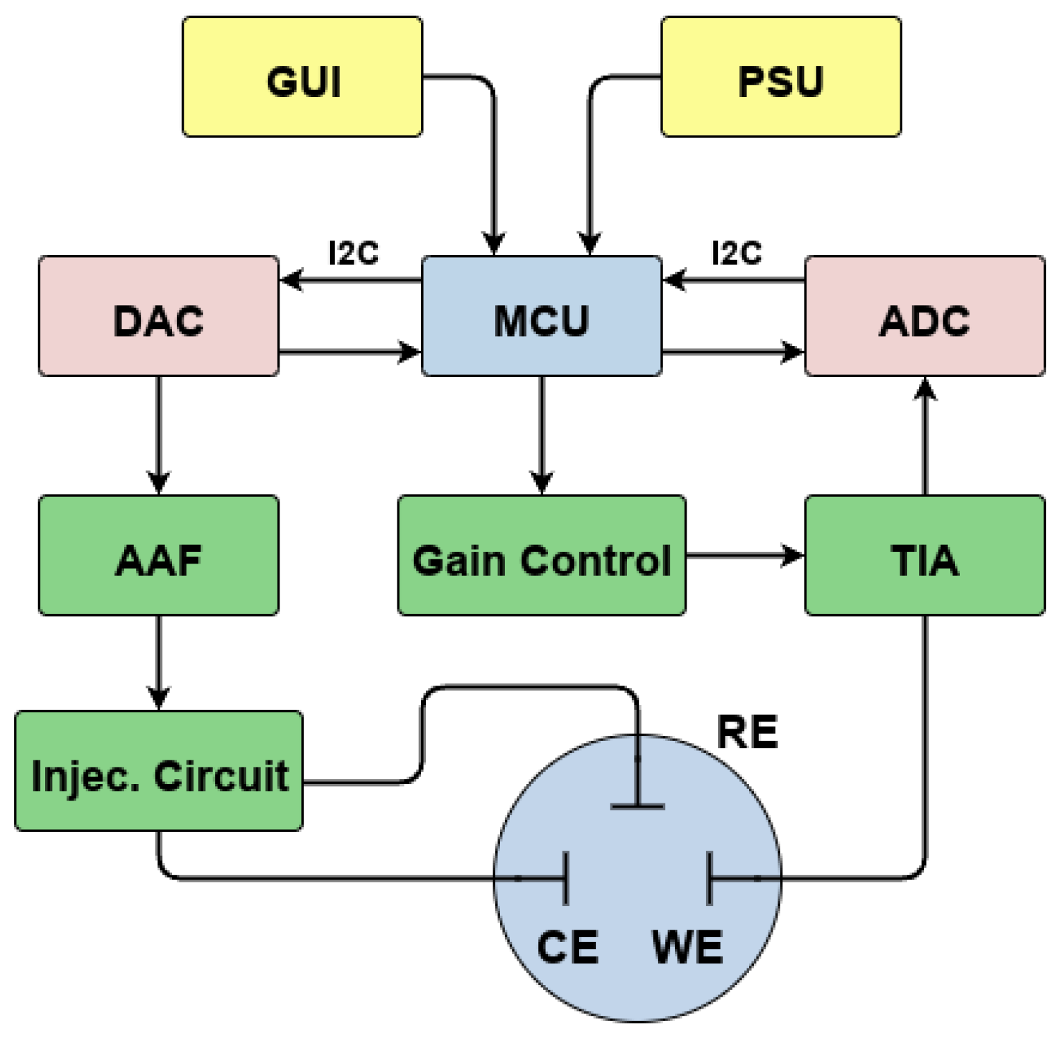
The design of this potentiostat aims to accommodate various electrochemical techniques that can be performed with the equipment. It is also designed to be a portable, user-friendly, all-in-one solution that operates independently of a computer running software. The block diagram of the instrument, illustrated in
Figure 1, shows the system components. It includes a digital-to-analog converter (DAC), an analog-to-digital converter (ADC), an anti-aliasing filter (AAF), a transimpedance amplifier (TIA) with gain control circuit, and a potential control circuit for the electrodes. It necessarily includes a microprocessor controller unit (MCU), which, for this design, should be able to run a general-purpose operating system, and a power supply unit to feed the entire instrument.
2.1. MCU Selection
The Raspberry Pi 3B+ (1.4 GHz 64-bit quad-core processor, dual-band wireless LAN, Bluetooth 4.2/BLE, faster Ethernet, and Power-over-Ethernet support (with separate PoE HAT) [
7]) was chosen for this project due to its numerous qualities that meet our requirements. The most important factor considered was its popularity and flexibility, which will enable the project to evolve in the future. It is a “credit card”-sized computer with a powerful processor and enough I/O capabilities as to satisfy the requirements of the actual design and further developments, in both software and hardware. It supports Debian-based optimized distribution for embedded systems, known as Raspian OS.
2.2. Electrodes Amplification Circuits
The potentiostat uses three electrodes topology to determine tiny variations in the impedance or conductivity of an analyte. For this, the instrument performs two tasks:
- (a)
It controls and measures the potential between the working and reference electrodes (WE and RE);
- (b)
It measures the diffusion current, which is defined as a flow of charged particles (electrons or ions) along a concentration gradient that flows between the WE and the CE.
It is important to distinguish here that, for the first task, the working electrode was tied to a fixed potential. Thus, the control of the potential was carried out by a feedback loop to maintain the desired potential between the WE and RE. If the potential deviates from the set value, the potentiostat adjusts the current flow through the CE to restore the desired potential. This feedback mechanism ensures that the potential remains constant, even as the electrochemical reaction proceeds and the resistance of the cell changes [
8].
Amplifier circuits include the electronics in charge of controlling the potential and measuring the current in a three-electrode system. The most critical is the working electrode circuit, because it is positioned where the electrochemical reaction of interest takes place. Therefore, it must have the highest sensitivity and the best quality components [
9].
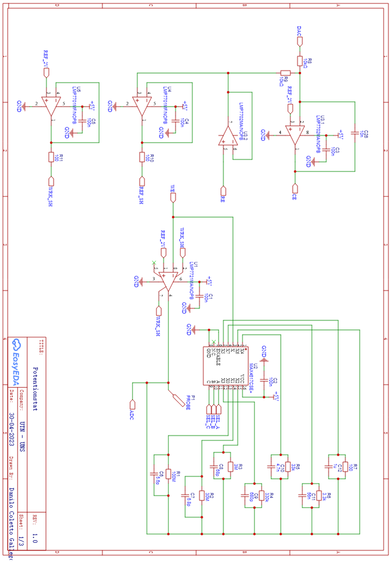
On the other hand, potential control can be designed as a feedback control system, where a potential is applied through the CE, and the signal is fed back through the RE. The system must be able to sweep potential values from −2.048 V up to 2.048 V, as this is the desired potential range this instrument should be able to handle inside the electrochemical cell during an experiment. To achieve this, two voltage references of 2.048 V (virtual ground) and 4.096 V are used. Further detailed explanations can be found in the following sections of this document. The images and circuits used in this document illustrate and describe the working principles that these circuits employ, and how they manage to perform the tasks they were designed for. Specific schematics circuits and software can be found in
Appendix B.
2.2.1. Summing and Buffer Amplifiers
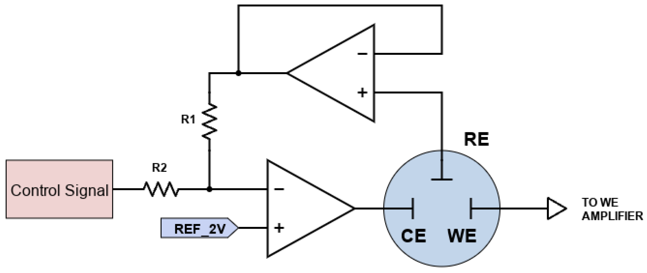
For potential control in the electrochemical cell, a simple inverting operational amplifier is used. A controlled potential from the Digital-to-Analog Converter (DAC) is applied to the negative inverting input through a resistor. The positive non-inverting input is connected to the circuit’s voltage reference, which is set at 2.048 V. This acts as a virtual ground, allowing for voltage excursions ranging from −2.048 V to +2.048 V from the perspective of the electrochemical cell.
To ensure that the reference electrode remains unbiased, a buffer circuit is implemented. In this setup, the reference electrode is connected to the positive non-inverting input of the amplifier, and the output to the negative inverting input of the counter electrode amplifier through a resistor. The high input impedance of the buffer circuit is particularly advantageous in this scenario. This circuit is illustrated in
Figure 2.
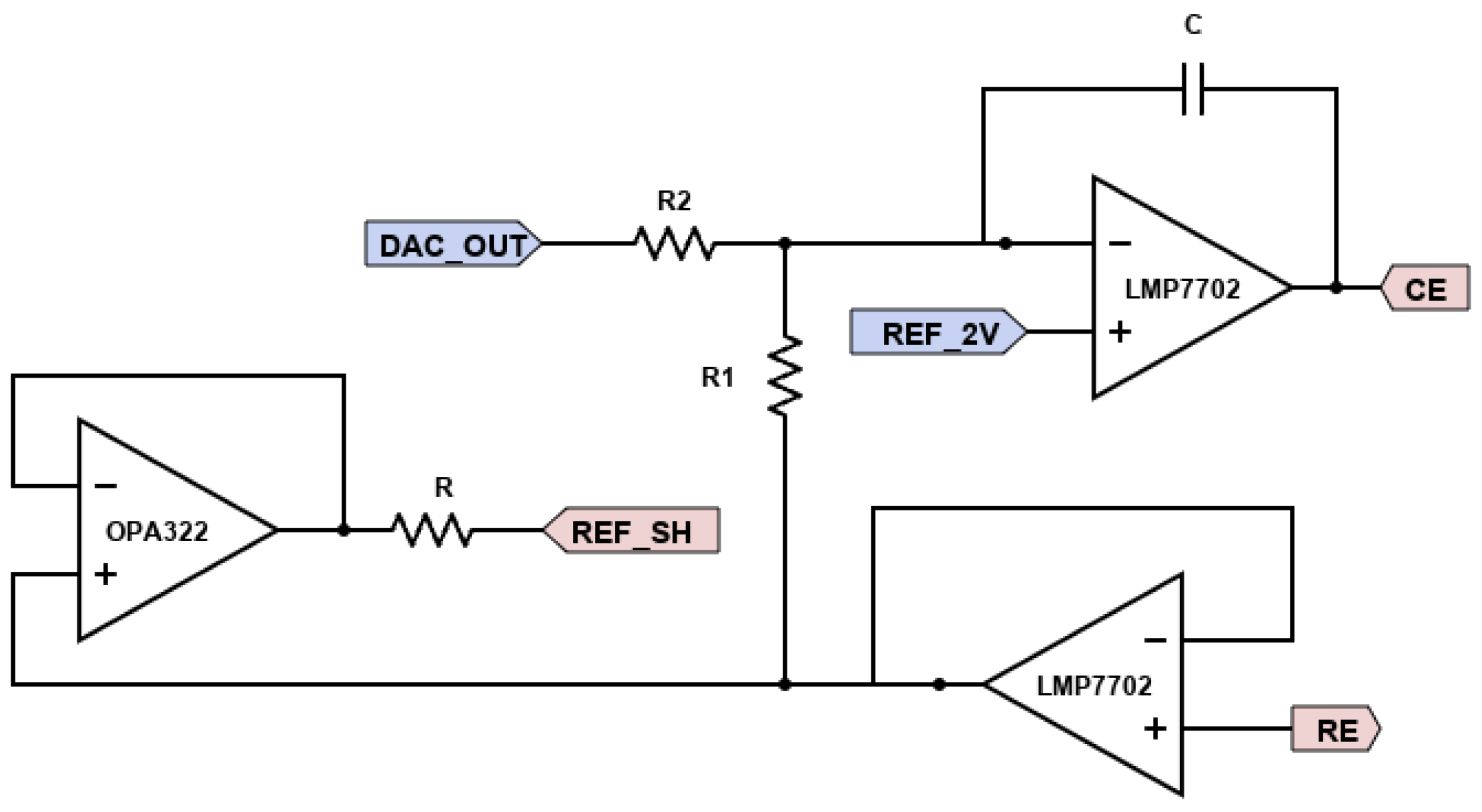
The RE provides feedback to the circuit. To prevent noise, leaks, or induced currents, the cable of this electrode is shielded and connected to a “Driven Shield” circuit [
10]. This circuit ensures that the shield of the cable is at the same potential as the core of the cable, which significantly reduces the leakage currents that flow through the insulation.
The amplifier selected for the counter and reference electrodes is the LMP7702MA [
11]. This choice was made due to its rail-to-rail capability, low input bias current, and high input impedance, all of which are advantageous for this application. For the shield circuit, similar amplifier characteristics are needed and can be found in amplifiers like LMP7701 [
11], OPA322 [
12], and OPA320 [
13].
Figure 3 shows the implemented circuit with more details.
2.2.2. Transimpedance Amplifier
The working electrode is where the electrochemical reaction of interest takes place. From the electronic point of view, the WE completes the circuit, allowing current to flow through it. To convert this current into a proportional voltage that can be read by an ADC later, a transimpedance amplifier is employed. In this setup, the positive non-inverting input is connected to a voltage reference, with the virtual ground set at 2.048 V. Meanwhile, the negative inverting input is directly connected to the WE and the amplifier output through a feedback resistor, which determines the gain of the amplifier. The output of the amplifier is linked to the ADC.
This component is one of the most critical parts of the equipment and must have specific qualities essential for precise and accurate measurements. For this task, LMP7721 [
14] was chosen due to its features as a precision amplifier, which include an extremely low input bias current, minimal voltage and current noise, high input impedance, and excellent isolation to prevent current leakage through the PCB.
In
Figure 4, it can be seen that this circuit also includes a “driven shield circuit” that connects to the shield of the working electrode cable. The LMP7721 package is specially designed to minimize leakage currents, making the implementation of guarding or driven shield systems simpler [
15]. OPA320 was used for this guarding shield, as in the schematic shown in the previous subsection.
Transimpedance gain is simply calculated by Equation (
1); in this amplifier configuration, it is directly the feedback resistor
.
Implementing a driven shield (active guard) via the OPA320 provides three critical advantages over a standard unshielded or grounded-shield design [
16]. First and foremost, it effectively eliminates leakage current errors [
17]. In a standard unshielded setup, any potential difference between the high-impedance input trace and the surrounding PCB (or ground) drives current through the insulation resistance; for example, even 1 G
of resistance at 5 V can leak 5 nanoamperes of current, completely swamping a femtoampere signal or even a few nanoampere signal. By driving the shield to the exact same potential as the input signal, the voltage difference across the insulation becomes zero (
), making the leakage current negligible, regardless of the insulation resistance (
).
Secondly, the driven shield neutralizes input capacitance through a technique called bootstrapping, while a passive grounded shield acts as a large capacitor connected to the input—which limits bandwidth and causes dangerous “noise peaking” (instability)—being an active shield moves in sync with the input signal. Because the voltage on the shield changes at the same rate as the voltage on the center conductor, no charge flows to charge/discharge the cable capacitance. This makes the effective input capacitance appear to be nearly zero, preserving the bandwidth of the TIA and maintaining stability.
Finally, the driven configuration acts as a Faraday cage, rejecting external electromagnetic interference (EMI) like 50/60 Hz hum, while also minimizing triboelectric noise generated by cable movement, since there is no potential difference to facilitate charge displacement.
2.3. Gain Selector
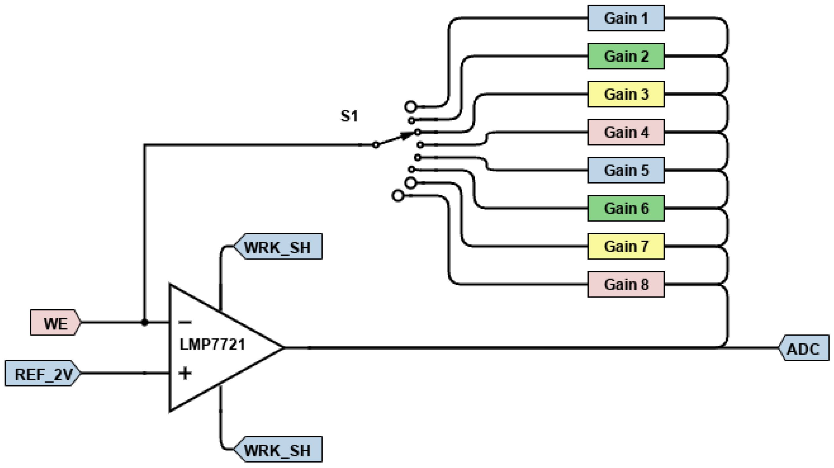
Changing the feedback resistor in the transimpedance amplifier allows the instrument to switch between different current operation ranges or scales. With higher resistance values, it can amplify and measure lower currents. To select these different gains, the MAX4617CSE, which features low off-leakage current, low noise, and high-speed operation, is an appropriate choice [
18].
The MAX4617CSE has eight channel inputs and one output. Selection is made using three digital control pins, which allow for eight possible combinations. The device is always enabled by connecting the ENABLE pin directly to the ground, as it is active when low. The eight feedback gain networks—each consisting of a feedback resistor and capacitor—are connected in parallel to the transimpedance amplifier output. Each network is routed to one channel input of the MAX4617, and the output from the multiplexer completes the feedback circuit through the negative inverting input of the LMP7721 amplifier. An schematic circuit is shown in
Figure 5 where the MAX4617 multiplexer is represented as a simple mechanical switch to facilitate the interpretation.
Calculating and selecting the appropriate feedback capacitor is critical because it plays a vital role in the stability and functionality of the circuit. This component helps prevent circuit oscillation, which can occur due to phase shifts caused by the input capacitance of the operational amplifier. Additionally, it regulates the bandwidth of the circuit and cut-off frequency, which are essential for filtering out unwanted high-frequency noise, thereby reducing noise amplification and enhancing signal integrity. This calculation can be easily performed using Equation (
2), and further insights can be obtained by applying the approximation described in Equation (
3).
To ensure that the amplifier operates within the desired bandwidth while filtering out high frequencies, it is important to use a capacitor that is lower than the limit set by the cut-off frequency. The instrument has a maximum working frequency of 100 Hz, so using a cut-off frequency of 1 kHz—ten times higher—follows common empirical practice.
2.4. Applied Potential: DAC
This equipment was designed to manage voltage potentials ranging from −2.048 V to 2.048 V. To achieve this, a DAC capable of handling potentials from 0 V to 4.096 V was required. This is because the entire circuit is referenced to 2.048 V, meaning that the working electrode in the electrochemical cell is actually experiencing a range from −2.048 V to 2.048 V, rather than the full 0 V to 4.096 V.
Another important factor to consider is the resolution of the DAC. The voltages produced by the DAC must be precise, since many electrochemical techniques require fine increments or steps. Therefore, resolution must be a key consideration in the design.
As proposed, the MAX5217SO08 [
19] is a suitable option. It is a buffered voltage-output, low-power DAC with a resolution of 16 bits. This provides a resolution of 62.5 µV and a quantization error of 31.25 µV, which is sufficiently small to meet laboratory needs and the requirements of most electrochemical techniques, such as cyclic voltammetry and square wave voltammetry. Furthermore, this DAC operates via an I2C interface, making it easy to manage with a Raspberry Pi, and has a low settling time, allowing it to handle higher frequencies when needed.
Antialiasing DAC Output Filter
The purpose of the filter, as its name suggests, is to soften the output signal of the DAC and to prevent aliasing or other unwanted components that may result from digital reconstruction entering the cell. Without this filter, abrupt small voltage spikes could occur at DAC output, which can lead to non-Faradaic current transient spikes over the WE. These spikes could potentially disrupt measurements, depending on the capacitance of the cell and the measuring speed used.
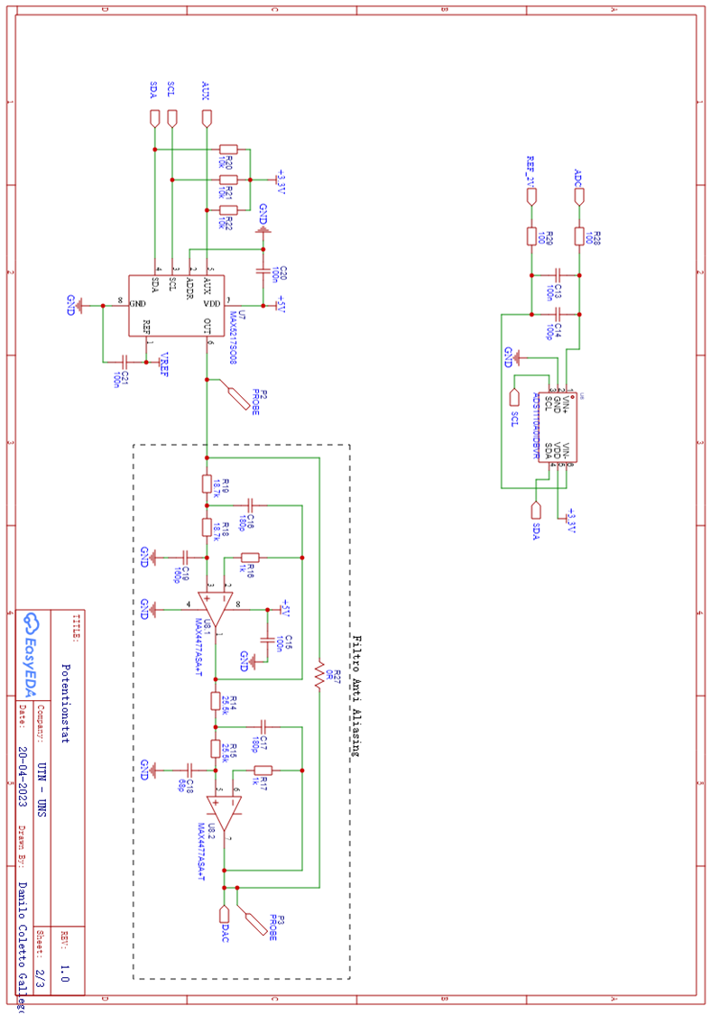
In this case, a fourth-order Sallen-Key [
20] anti-aliasing filter was employed, with a cut-off frequency of 35 kHz, which was initially designed for higher working frequencies. This filter also helps prevent potential voltage glitches that may arise when switching the DAC’s output applied to the cell. For this filter design, the MAX4477ASA+T [
21] was used because it contains two identical operational amplifiers that fulfill the filter requirements. The filter topology is displayed in
Figure 6.
2.5. Sample Acquisition: Analog to Digital Converter
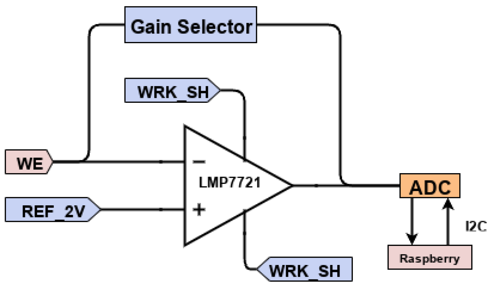
To measure the voltage proportional to the current in the cell, an ADC is connected to the output of the transimpedance amplifier (
Figure 7). An ADS1110 [
22] was used for this purpose; it is a 16-bit ADC with a maximum sampling frequency of 240 SPS, utilizing I2C communication.
The ADS1110 features a delta–sigma converter with a differential input and an internal reference voltage of 2.048 V. It can operate at four different sample rates, although higher rates come with a slight reduction in resolution: 16 SPS offers 16 bits, 30 SPS provides 15 bits, 60 SPS gives 14 bits, and 240 SPS allows for sampling at 12 bits. Additionally, an internal programmable gain amplifier is available, which can be configured with four preset gains: 1, 2, 4, and 8.
To configure ADS1110, an 8-bit register is used that allows for both writing and reading. Bits 0 and 1 are designated for configuring the Programmable Gain Amplifier (PGA). Bits 2 and 3 are used to select the sample rate. Bit 4 determines the sample mode, which can either be continuous or single conversion. Lastly, bit 7 serves as a flag to indicate the start of a new conversion or sampling when written; it can also be read to check whether the data in the output register is new or outdated. Bits 5 and 6 are reserved and must be set to zero.
2.6. Power Supply and Voltage References
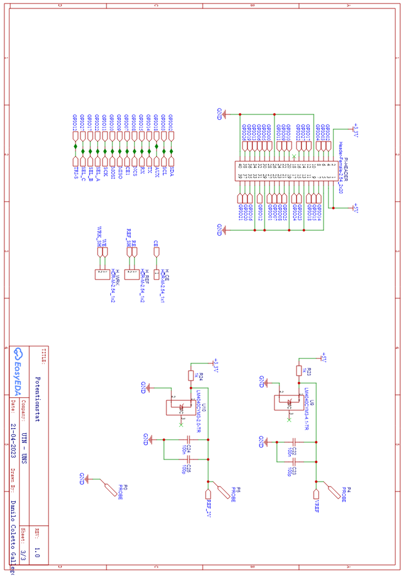
Power is supplied by the Raspberry Pi through the 5 V and 3.3 V lines. The 5 V bus powers all +5 V integrated circuits (ICs) and the voltage references, while the 3.3 V bus is dedicated to powering the pull-up resistors used in I2C communication devices.
To generate the stable voltage references of 2.048 V and 4.096 V needed for analog-to-digital converters (ADCs), digital-to-analog converters (DACs), and amplifier circuits, the LM4040CYM3-2.0 and LM4040CYM3-4.1 [
23] reference voltage devices were employed, respectively.
2.7. Software
Initially, the entire control software was intended to be coded in Python. However, as the development of the equipment progressed, some issues with the operating system began to arise, highlighting the need for precise control over the microprocessor. Certain functionalities, such as square wave generation, required accurate timing control, which sometimes conflicted with the performance of the operating system. As a result, the main control firmware of the system was developed in C, as the lower-level libraries provided us with better control over these critical aspects.
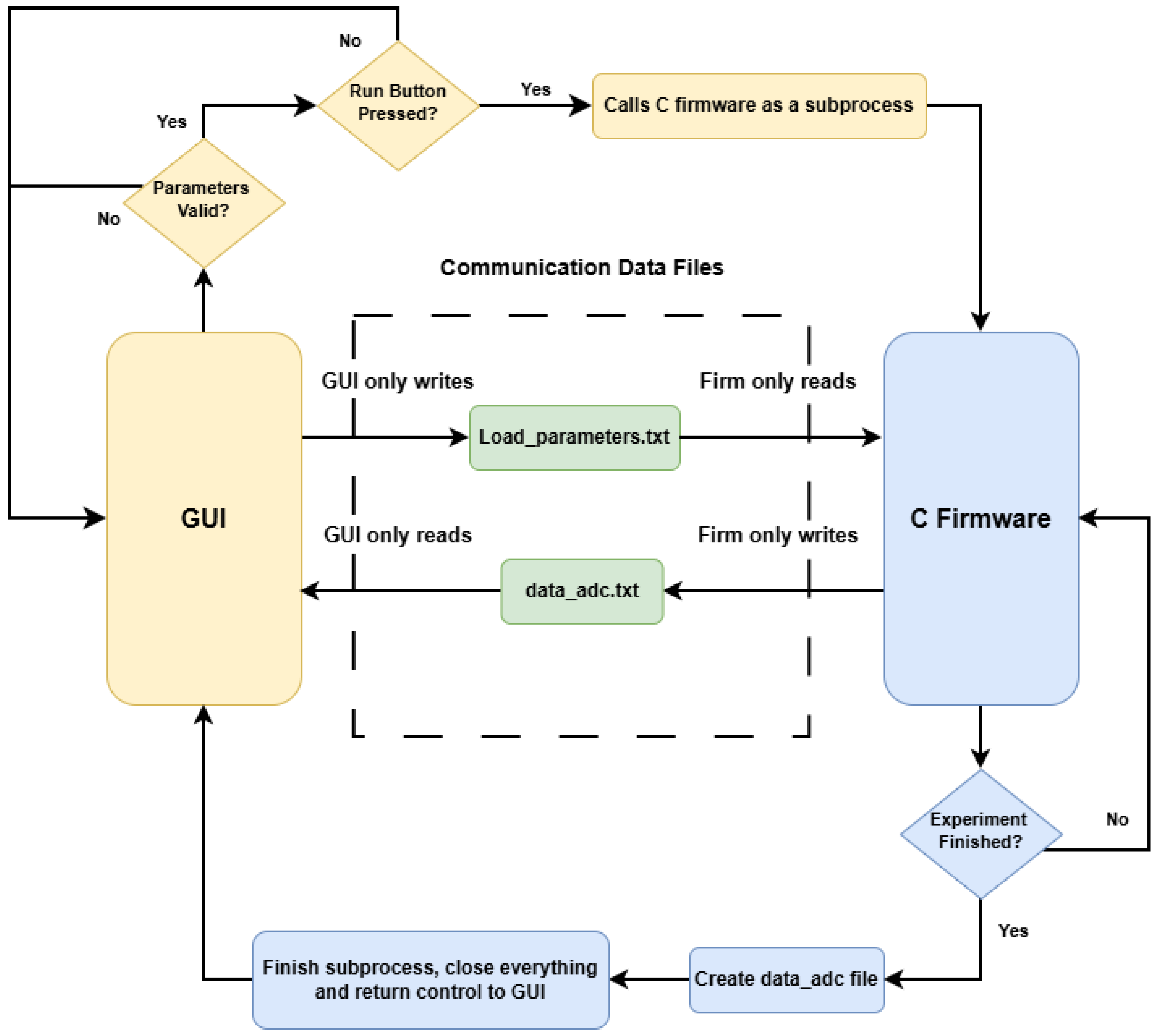
To maintain simplicity, communication between the GUI and the firmware relies on a text-based file exchange mechanism. The GUI generates a configuration file, Load_parameters.txt, which is strictly write-only for the GUI. The firmware reads this file upon initialization to load the experimental parameters but does not possess write access. Conversely, the firmware logs all measurement data into data_adc.txt. This file is write-only for the firmware; once the acquisition process concludes, the GUI parses this file to update the graphical visualization.
Access to
Load_parameters.txt and
data_adc.txt is strictly synchronized to prevent race conditions. Simultaneous read/write cycles are impossible because the firmware is executed as a blocking sub-process of the GUI. Control returns to the GUI only after the firmware has completed its execution and terminated. This sequential workflow is illustrated in
Figure 8. Further details regarding the GUI and internal software architecture are provided in
Section 2.7.7 and Section Software Operation.
2.7.1. Firmware
This is the main code that controls all the peripherals on the potentiostat board, including the ADC, DAC, and gain selector. It utilizes a series of specially written libraries to achieve this functionality. The program reads the data that the user loads into the GUI, configures the equipment with the specified parameters, and executes the experiment. Once the experiment is completed, the code saves the resulting data to a file and then returns control to the GUI.
The firmware relies on four primary libraries, which are as follows:
ADC – ADS1110 – Library;
DAC – MAX5217 – Library;
Timer Control Library;
‘General_Setup’ Library.
2.7.2. ADC Library
The library ioctl from Linux was utilized to implement I2C communication, as it enables more direct interaction with the Raspberry Pi I2C bus.
The ADS1110 communicates using three bytes in big-endian format (most significant byte first). The first two bytes represent the output buffer of the ADC, while the last byte contains the configuration of the device. For proper operation, the firmware must consistently request all three bytes from the ADC; it will respond with the complete set of data. Once all the data is received, the relevant information can be extracted, and the rest can be discarded. In contrast, writing data is simpler, as only one bit can be written to ADS1110, which has a single writable register.
The most important function of this library is the one that reads analog data and returns a value in millivolts. This is important because the resolution of the ADC varies depending on the sample rate. Therefore, if the sample rate is altered, the ADC resolution will also change, requiring accurate interpretation of the data.
2.7.3. DAC Library
This library is simpler than the ADC library because it uses the
wiringPiI2C library internally, which streamlines the communication process. It includes functions that accept parameters such as the device address, the command to send or execute, and the data to transmit to the device. This aligns perfectly with the communication format and protocol required by MAX5217 [
19].
The library is designed for a little-endian (least significant bit) format, while the DAC expects data in big-endian format. To address this discrepancy, a straightforward bit inversion operation is necessary for the data before it is sent to the device.
2.7.4. General Setup Library
This section of the code includes generic and straightforward functions utilized by the system in various scenarios. These functions consist of initialization, reading and writing operations, and memory management for dynamic arrays. Additionally, functions for gain selection and control pins are implemented in this library using the wiring library for GPIO (general-purpose input/output) control.
2.7.5. Timer Control Library
The core of the firmware is implemented in this library, which contains functions to control the timer—specifically to configure, initiate, and stop it, along with its handler. Additionally, it includes functions to determine the type of experiment the instrument needs to perform and how to load and set the experiment parameters. The various techniques for running the experiments are also included in this library.
One of the most important functions defined in this library is function_initializer. It receives configuration data, prepares the entire device for executing the procedure, and initializes the timer. During the test, the program enters a while loop, as the timer now calls the actions that need to occur. Once the timer finishes, a variable used as a flag is set to indicate that finalization is required, which allows the program to exit the loop. The timer is then stopped, and the program returns to the main function, exiting from function_initializer.
2.7.6. Main Code
The main code is responsible for reading the configuration file prepared by the GUI and saving that data into an array. It then calls function_initializer, passing the configuration array as a parameter. Once the experiment has concluded, the main code stores all the sample data into a file, closes all processes, and frees any previously allocated memory. Finally, the program completes its execution and returns control to the GUI.
2.7.7. Graphic User Interface
The user interface needed to address several key aspects regarding user experience. The major considerations included the following:
The ability to configure parameters easily and execute experiments seamlessly through the graphical user interface (GUI).
Results should be easily visualized or previewed via graphics provided by the interface.
Users should have the capability to smoothly extract data in a simple yet useful format compatible with Excel or similar software.
In addition to user-focused concerns regarding the interface, several factors were taken into account during the development process, particularly the need for efficiency and simplicity in programming. With this in mind, the decision was made to use the Tkinter library in Python. It offers a variety of tools, such as notebooks, canvas, buttons, plots, entry widgets, and message boxes, which facilitate the rapid development of a straightforward interface from scratch.
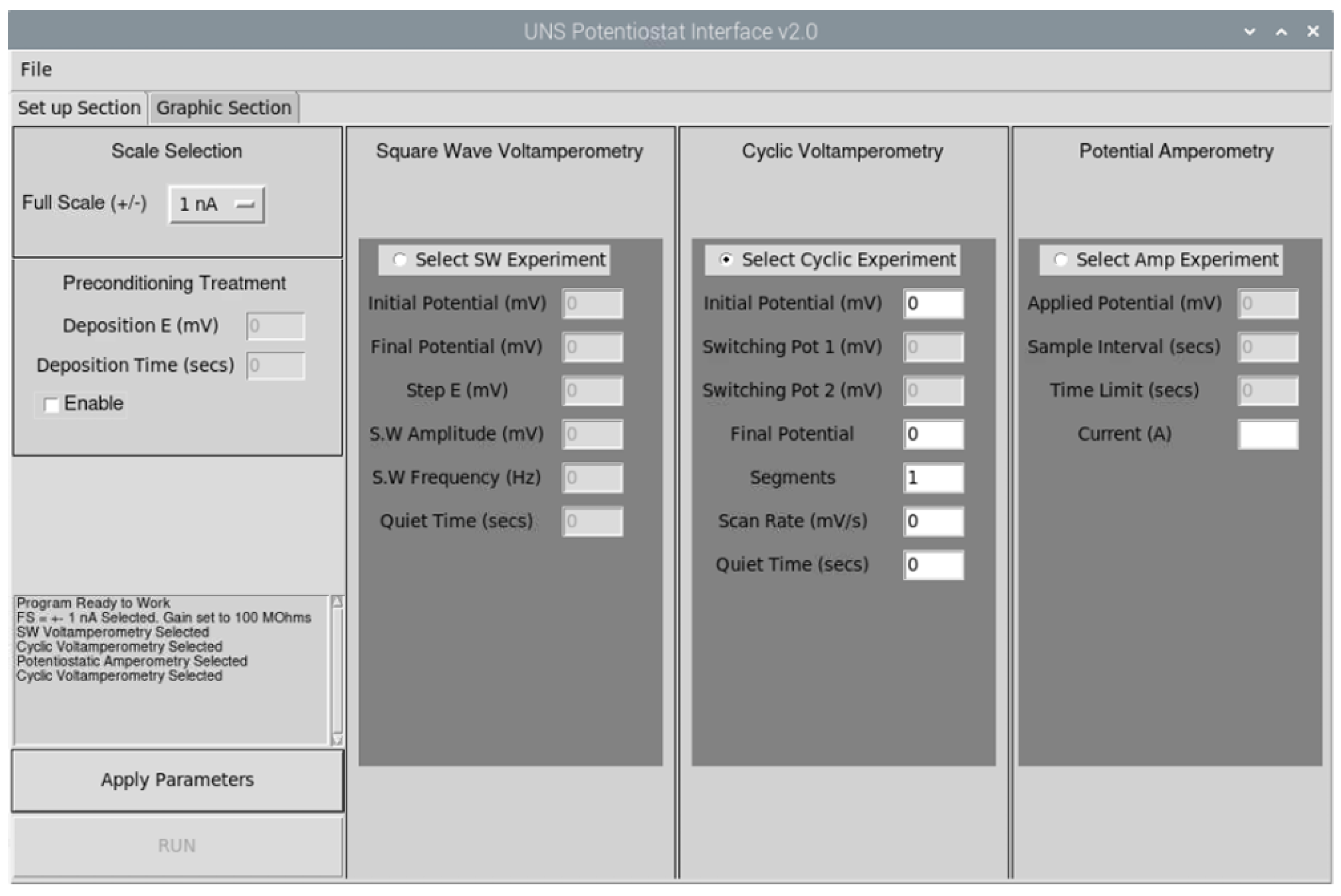
The resulting graphical interface features two main sections. The first section is the “Setup” area, where users can find all the options available for configuring and executing an experiment (
Figure 9).
3. Build Instructions
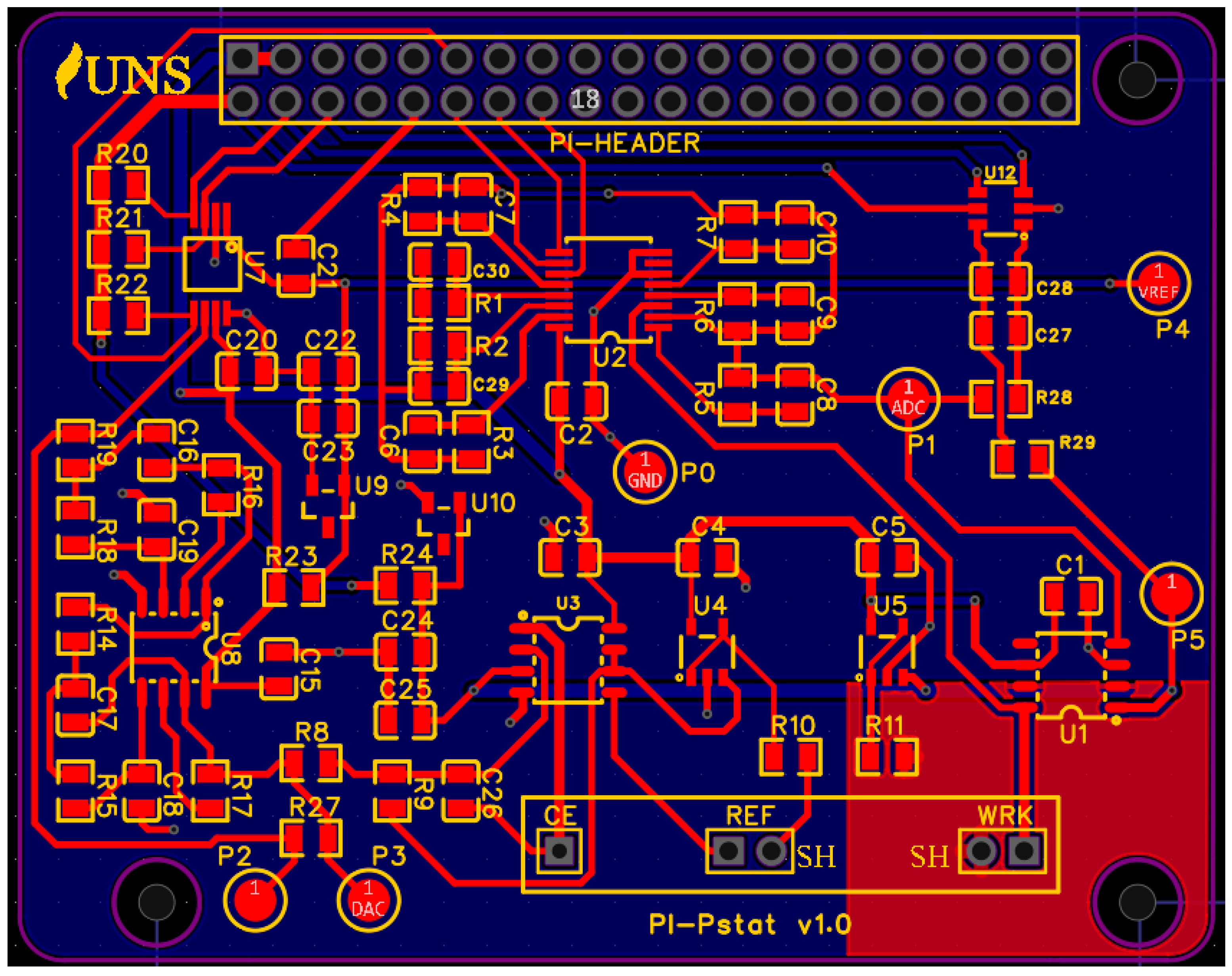
While designing the printed circuit board (PCB), it was essential to explore effective techniques for low-current circuit design. This step is crucial during the design phase, as it significantly impacts the final capabilities and precision of the instrument. The PCB schematics and the board (
Figure 10) were created using EasyEDA [
24], an open-source and free alternative that streamlines the design and fabrication process. EasyEDA provides a comprehensive solution that includes designing, generating the bill of materials (BOM), producing the necessary files, and facilitating the ordering of fabrication services.
The building process will be reviewed in this section, from hardware up to the software development, but every file necessary for the proper replication of this project will be available in the
Supplementary Materials.
Table 1 summarizes the main components needed, their sources, and the project’s general costs.
3.1. Hardware
The Bill of Materials for the design and construction of the PCB is listed on
Table 2.
3.1.1. PCB Assembly
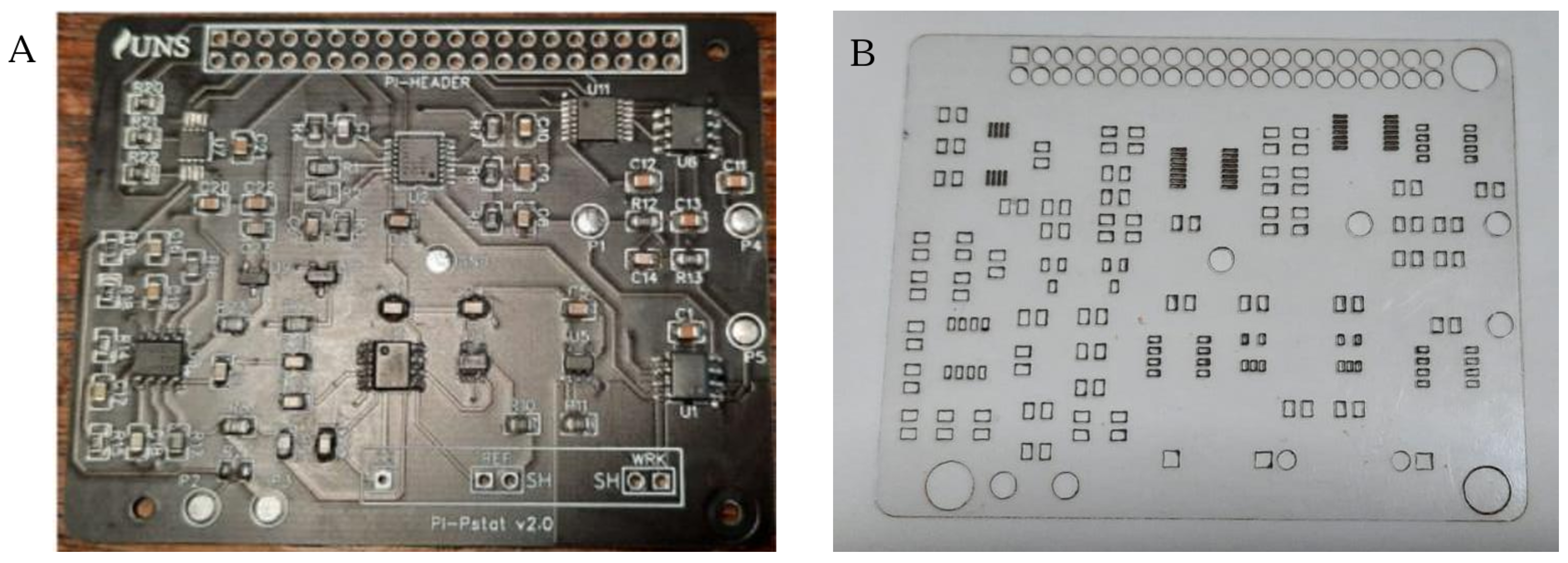
After the PCB arrived, it was manually assembled with its SMD components (
Figure 11A). A simple hot-plate soldering station was developed for this purpose. Since a steel stencil was not ordered with the PCB, a custom stencil was fabricated to apply the right amount of solder paste in the correct locations. This stencil was created using a laser cutting machine set to a low-power configuration and made from a 1 mm acetate film (
Figure 11B). Once the stencil was complete and the solder paste was applied, the SMD components were placed, and the hot plate was used for the re-flow process. However, small adjustments were necessary, and the quality of the solder joints was closely monitored. At this stage, pins and connectors were also soldered.
3.1.2. Case Design
A small case was designed using Autodesk Fusion 360 [
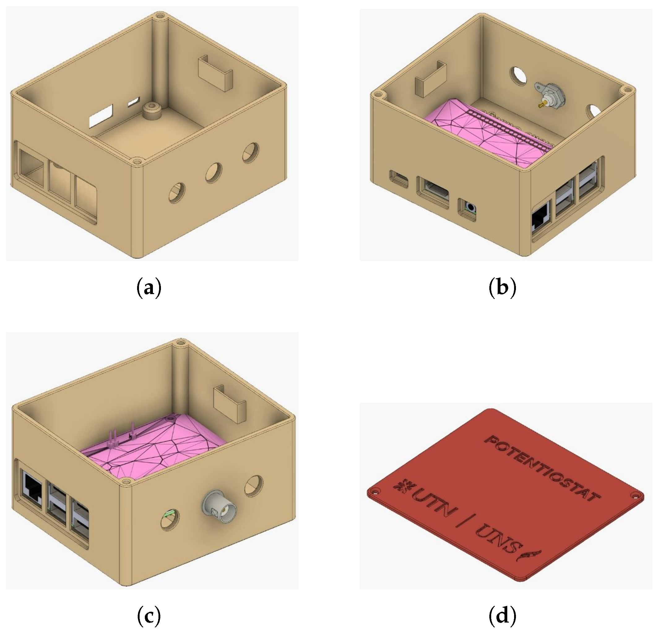
25] to accommodate both the Raspberry Pi and the PCB. The case needed to support BNC connectors for electrodes while maintaining a compact design. The final product is a small box with a lid that is secured with screws at the top. It features holes for the power, USB, HDMI, and Ethernet connectors of the Raspberry Pi. Ultimately, the case was 3D printed, and the design files are available for download in the
Supplementary Materials. The whole case design can be in
Figure 12.
3.1.3. Final Assembly
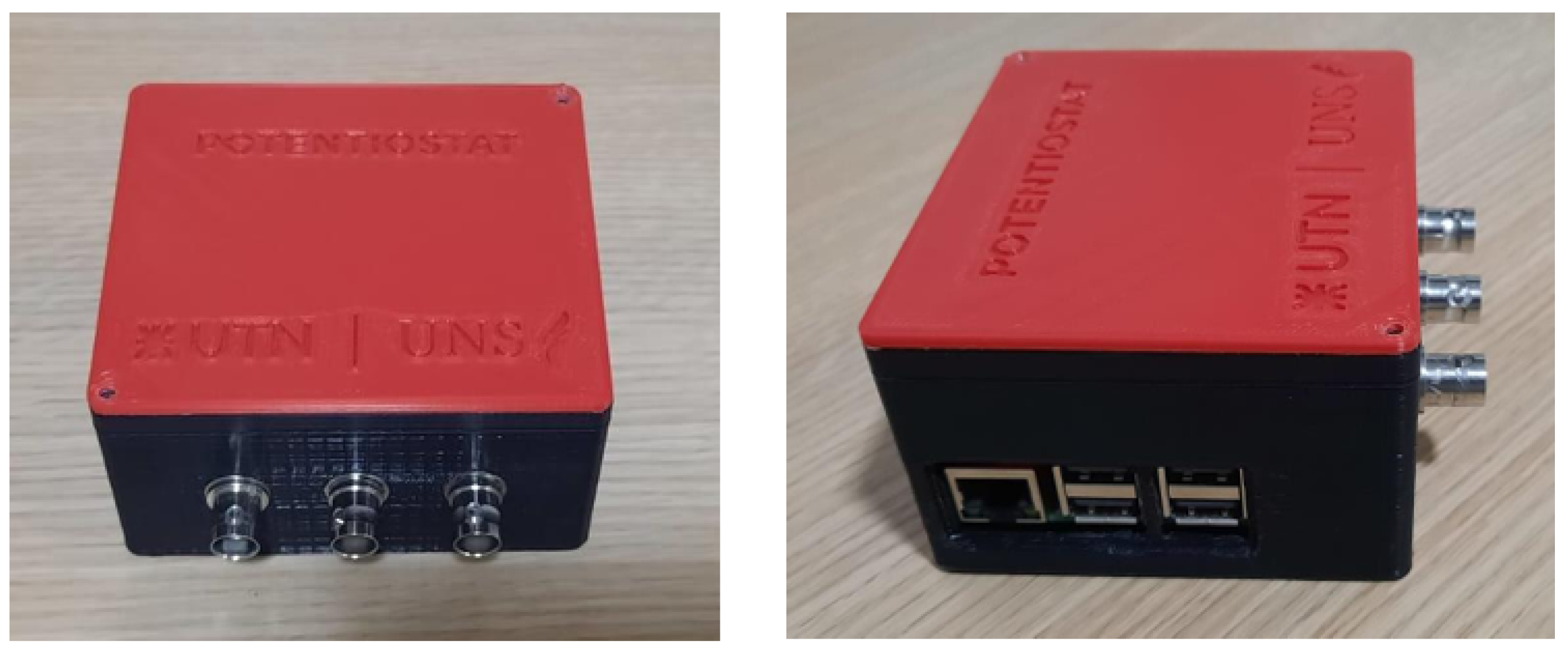
The potentiostat PCB is mounted on top of the Raspberry Pi and connected to it using a female pin header connector. BNC connectors are installed in the case and linked to the PCB with cables. The final step is to place the entire system inside the case and secure the cover with screws.
Figure 13 presents the assembled instrument.
3.2. C Libraries Installation
The main control firmware of the system was developed in C, as the lower-level libraries provided us with better control over these critical aspects.
So, in this section, there are some commands that may be useful for those users who shall try to install the software and replicate the instrument. This little command list may simplify the compilation of the C files into a single file to be executed by the Python interface.
git clone https://github.com/WiringPi/WiringPi.git
cd WiringPi
git pull origin
./build |
% First option is to use the GCC Compiler and include just every C Library
% specifying the path where it is placed and using the commands -lm and
% -lwiringPi to also include in the compilation the standard math and
% WiringPi libraries
% At the end, the user must define the name that the generated file will get
gcc Prueba_Completa01.c Libraries/libsetup/general_setup.c Libraries/libtimer/timer_version5.c Libraries/libdac/DAC_enC.c Libraries/libadc/ADC_I2C.c -lm -lwiringPi -o program_code_v1.x
% A Second option may be compiling each file into an object file
gcc -c general_setup.c -o general_setup.o
gcc -c timer_version5.c -o timer_version5.o
gcc -c DAC_enC.c -o DAC_enC.o
gcc -c ADC_I2C.c -o ADC_I2C.o
% Then, linking all the object files into an executable
gcc general_setup.o timer_version5.o DAC_enC.o ADC_I2C.o -lm -lwiringPi -o myProgram |
% This command allows to change the program priority
sudo nice -n "valor" -p "PID"
% This command allows to change the program priority on the run
sudo renice -n "valor" -p "PID" |
4. Operating Instructions
The instrument exhibits significant sensitivity to 50 Hz line noise within the low current ranges (1 nA, 40 nA, 100 nA, and the lower end of the 1 µA scale). This susceptibility is particularly pronounced during the square wave voltammetry experiments due to the technique’s rigorous timing and sampling demands; conversely, cyclic and linear voltammetry appear to be almost not affected. Therefore, it is highly recommended to isolate the equipment from line-powered noise sources—such as computers, power supplies, and LED lighting. Furthermore, powering the instrument via a battery or power bank is advisable to minimize interference and enhance portability. This configuration was utilized for the experiments described in
Section 5 and
Section 6.
There are two primary ways to interact with the potentiostat. The first option is to use a remote desktop application, such as RealVNC, which is already integrated into the Raspberry Pi OS. The second option is to connect a monitor, keyboard, and mouse to the Raspberry Pi, allowing it to function like a standard computer; while these are not the only possibilities, they are the simplest and most suitable methods.
Software Operation
The software interface can be accessed through the command line using a simple command, after which the operations can be conducted via the graphical user interface (GUI). In the first screen, users can choose from two techniques currently offered: cyclic voltammetry and square wave voltammetry. These techniques enable the use of electro-deposition or pre-treatment for implementing anodic re-disolution voltammetry. Once a treatment is selected, the relevant parameters become visible and can be filled in, and the scale can also be chosen within this part of the interface. The operator must understand the expected responses from the experiment in order to properly configure the current scale, as this is crucial for determining whether the results are appropriate.
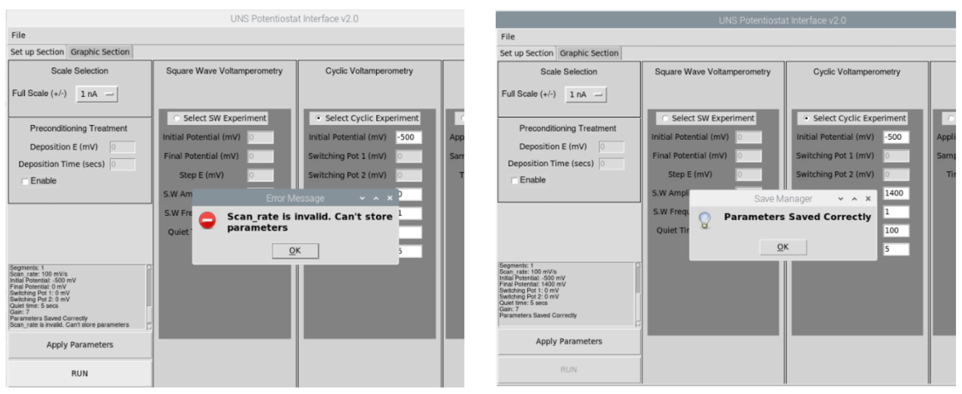
Once the user has set all parameters, clicking the
Apply Parameters button verifies that the entered values are valid as shown in
Figure 14; they must fall within the allowed range and cannot be blank. If everything is correct, this setup is saved, and a configuration file for the firmware is generated. The user can view the complete saved configuration through the console. Finally, the
RUN button becomes enabled, and the system is ready to execute the experiment. During this process, the interface may appear to be “frozen”, but it continues to operate in the background.
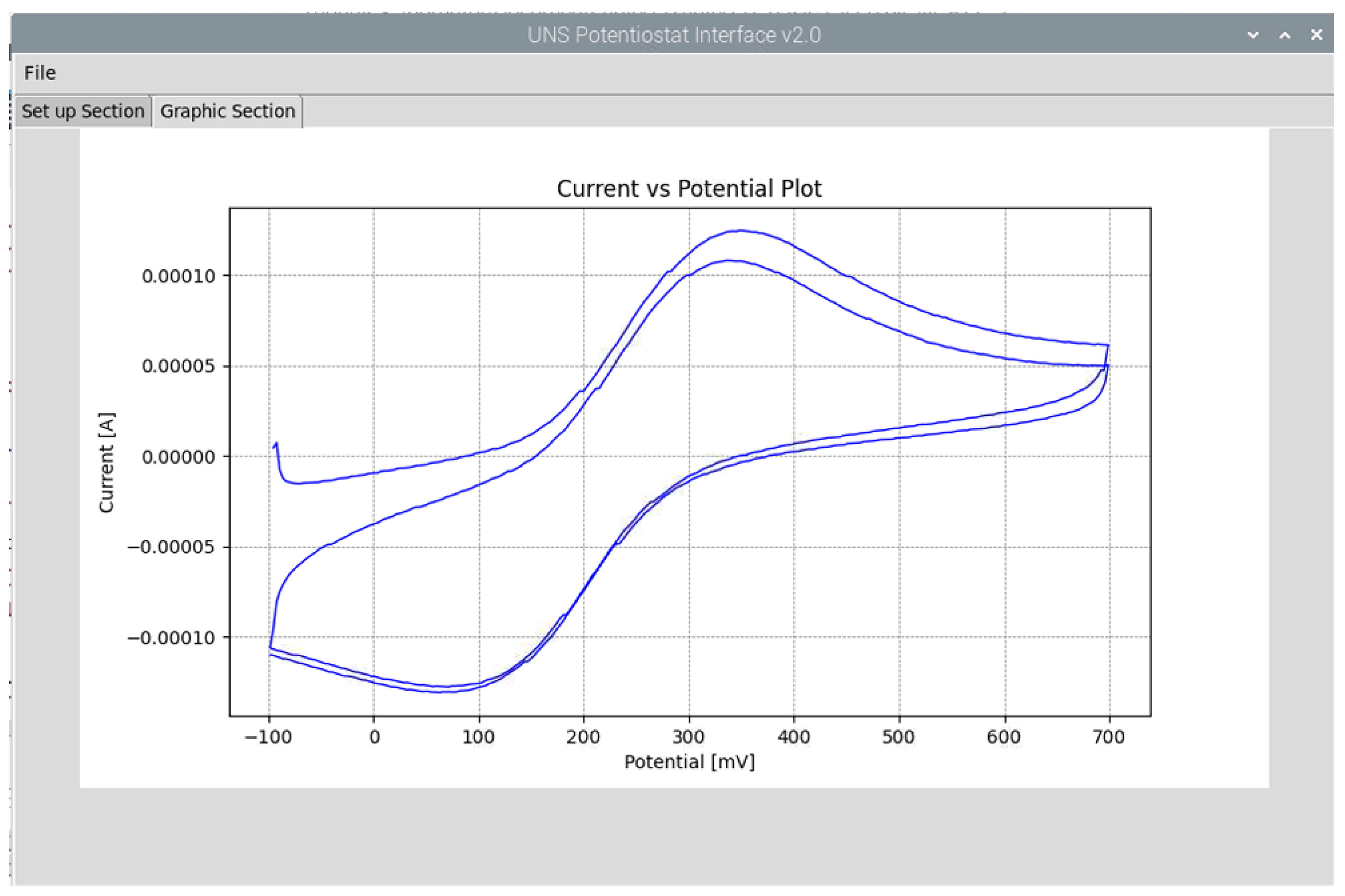
When the execution is finished, a message box will appear to notify the user, who can then view the preliminary results in the graphic section. In the “Graphic” section, the collected results are displayed in a simple graph that plots Potential (measured in millivolts) against Current (measured in amperes). The scale of the graph is automatically adjusted, allowing the user to quickly and easily view their measurements without needing to worry about the scale. The view of this graphic section is displayed in
Figure 15.
Furthermore, in the right upper corner, there is a drop-down menu named “File” that will allow the user to save the collected samples in a plain text file (
Figure 16).
5. Validation
To evaluate the instrument, several preliminary tests were conducted before carrying out a real application experiment. The first set of tests involved checking for linearity using a range of resistors with known values. This allowed for the measurement of known current values and assessment of the instrument’s linear response for various gain settings. As a result, the linearity of the current measurements was confirmed, and minor software corrections for the gains were made if discrepancies between the actual and expected gains were identified—essentially calibrating the instrument.
The second series of tests utilized an actual electrochemical cell with specific “pattern” solutions that had known characteristics and responses. For these tests, potassium ferrocyanide and potassium chloride solutions were used, employing cyclic voltammetry as the methodology.
All tests, both with the dummy resistors and the pattern solutions, were replicated using commercial equipment available at the Shared Use Instrumentation Laboratory (LIUC) of the Universidad Nacional del Sur (UNS). This equipment is an Epsilon 2 from Bioanalytical Systems, Inc., which allows the comparison and verification of the performance of the laboratory-made instrument.
5.1. Linearity Tests
The evaluations were conducted using the various gain scales of the instrument, which correspond to the different feedback resistance values of the gain selector. The appropriate scale depends on the intensity of the currents to be measured. In this report, we will present only some of the linearity tests, focusing on the most critical ones, those that push the equipment to its limits with low currents, and those with the best results. The dummy cell resistors used for testing are displayed in
Table 3.
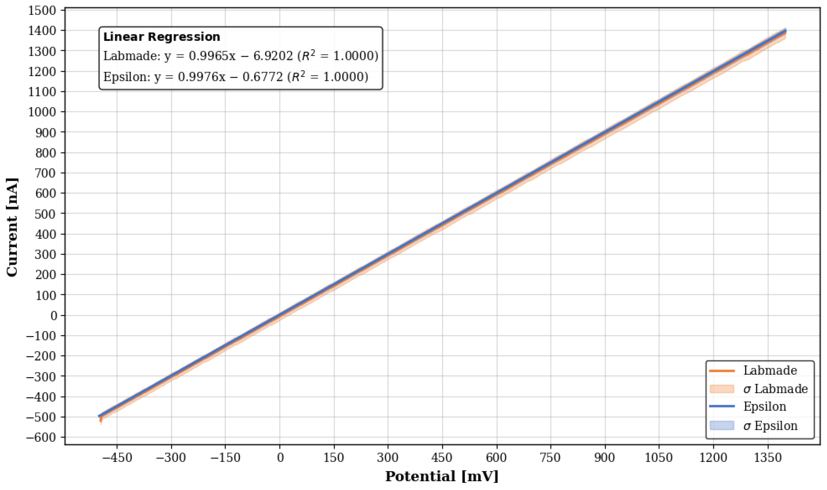
Figure 17 illustrates the mean response curve of a test conducted from −500 mV to 1400 mV across a 1 M
resistor (the test was replicated 5 times for each equipment,
n = 5), resulting in expected current measurements ranging from 500 nA to 1.4 µA in a single gain scale (10 µA gain scale for this case), demonstrating a good linear response. The figure also includes a comparison of the response of the commercial equipment with that of the lab-made potentiostat. The mean standard deviation was 20.7046 nA for the lab-made potentiostat and 10.2988 nA for the commercial instrument. The linear regression equations are also calculated for both the lab-made instrument [
4] and the commercial equipment [
5].
This test were conducted for the different scales of the instrument in order to verify the linearity of the whole set of current scales. In
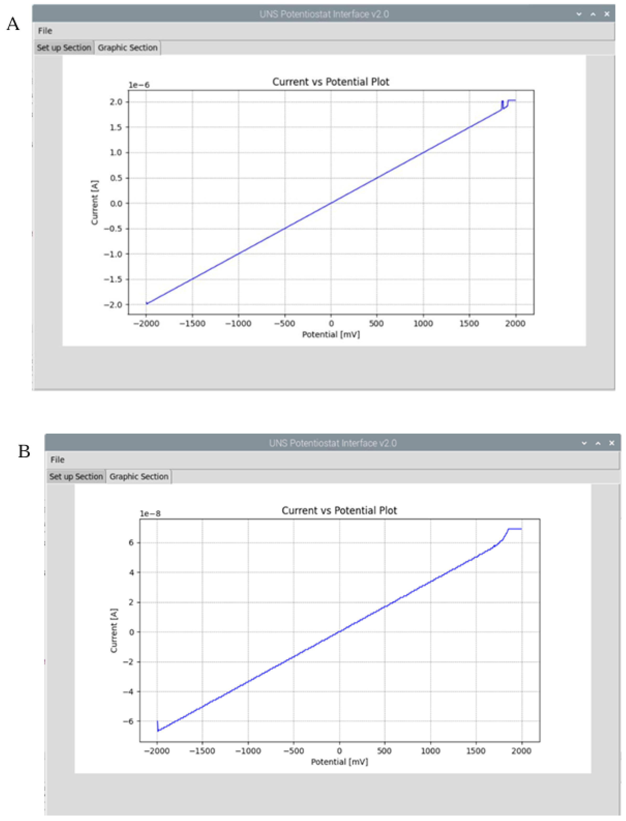
Figure 18, the results of linearity experiments are displayed for dummy cells of a 1 M
resistor and a 30 M
resistor, as shown on the instrument’s graphic interface. These images illustrate the loss of linearity at the upper limit of the amplifier’s range for those gain scales (which are, 100 nA current scale for the 1 M
resistor test and 10 µA current scale for the 30 M
resistor test) but also a good response in almost the entire range and for two different orders of magnitude of current (nA and µA). Approximately 98.5 % of the scale (using this gain) is perfectly linear, which is more than acceptable.
Linear regressions equations and R
2 coefficients were calculated for
Figure 18A in [
6] and
Figure 18B in [
7] using the data recorded the during experiment.
It is important to note that this test was conducted using a simple linear sweep from an initial voltage to a final voltage. Additionally, linearity verifications were also performed for the square wave voltammetry technique.
5.2. Pattern Solutions Tests
After calibrating the instrument and testing its linearity with dummy cell experiments, tests were conducted using pattern solutions with well-established characteristics and responses. These solutions are typically utilized as calibration tools and references in chemical experiments, making them ideal for evaluating the potentiostat and comparing it with the commercial instrument.
For these experiments, the focus was exclusively on Cyclic Voltammetry to obtain voltammograms that characterize the redox chemical reaction. As previously mentioned, solutions of potassium ferrocyanide and potassium chloride were prepared and tested. The resulting voltammograms illustrate an oxidation/reduction cycle, where peaks for the cathodic current—represented by a positive peak indicating the analyte reaching its reduction potential—and the anodic current—represented by a negative peak indicating the analyte reaching its oxidation potential—are clearly distinguishable.
The electroactive solution consisted of 7.5 mM potassium ferrocyanide (), while 0.1 M of potassium chloride (KCl) solution served as the supporting electrolyte (this mean it will not react in the cell). Experiments were conducted in a 25 mL electrochemical cell using a three-electrode configuration. This setup comprised a polished glassy carbon electrode (GCE) as the working electrode (WE), a platinum spiral as the counter electrode (CE), and a (3M ) electrode as the reference electrode (RE).
All measurements were performed in quintuplicate (). The Cyclic Voltammetry parameters were identical for both solutions and set as follows:
Initial potential: −100 mV.
Switching potential: 700 mV.
Final potential: −100 mV.
Scan rate: 100 mV s−1.
Quiet time: 2 s.
Table 4 summarizes the experimental conditions for the pattern solution tests.
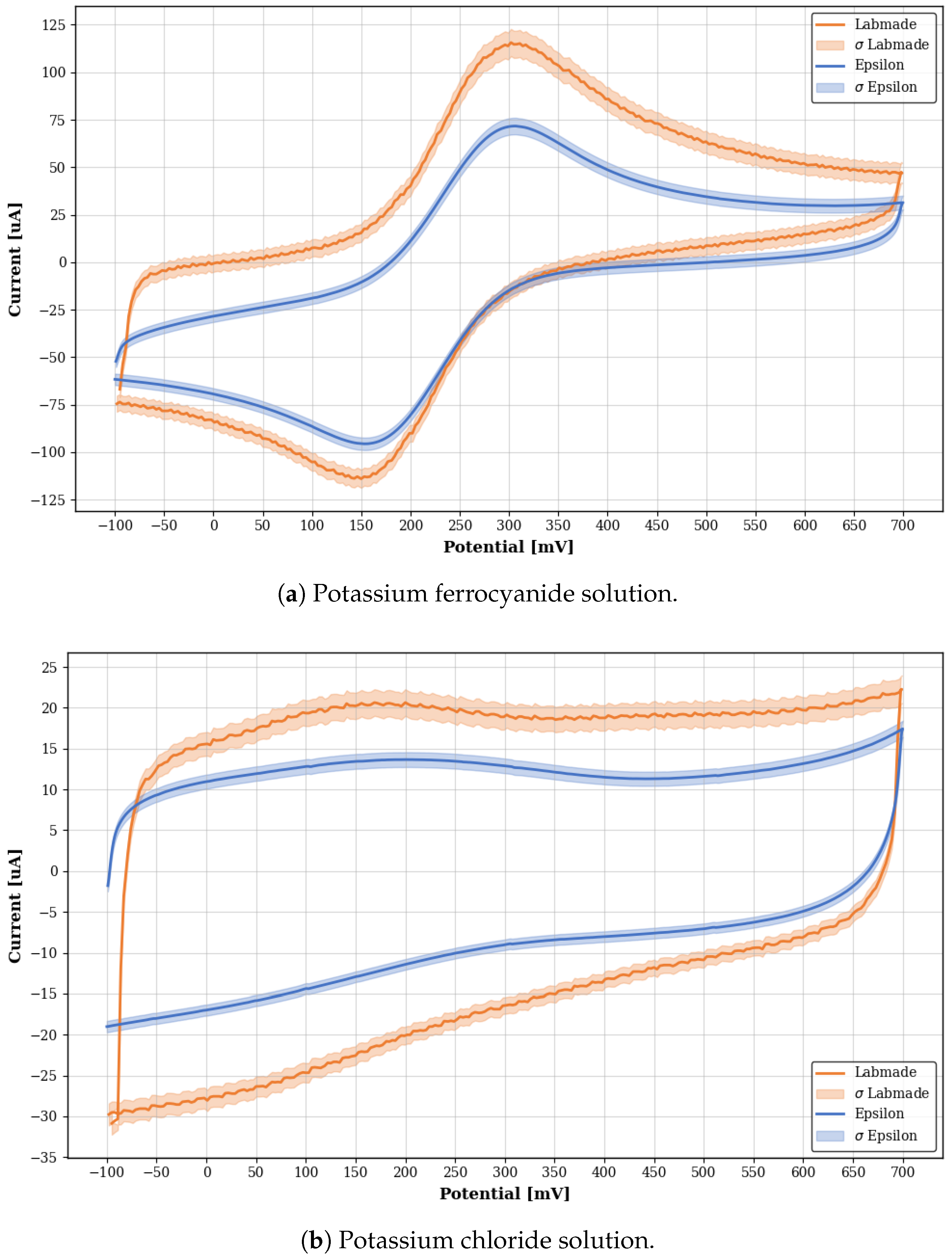
Figure 19 displays the mean voltammograms (
n = 5) for both potassium ferrocyanide and potassium chloride. The figures show the voltammograms obtained from the lab-made and commercial instruments.
Cyclic voltammetry is primarily used as a qualitative technique. Therefore, the main objective of these experiments was to obtain a response pattern and shape from the lab-made instrument that was comparable to that of the commercial instrument. It is important to note that current intensity is not solely a property of the instrument; it heavily depends on the solution being measured and the condition of the electrodes. In particular, the working electrode requires perfect polishing and thorough cleaning between experiments to ensure accuracy.
However, it is still possible to compare the current intensities quantitatively. Potassium ferrocyanide acts as the electroactive solution, while potassium chloride serves as the electrochemically inert solution within this scan range. As shown in
Figure 19a, the oxidation (positive spike) and reduction (negative spike) potentials appear at 150 mV and 300 mV, respectively. At these points, the lab-made equipment exhibited higher current responses, with differences of 19.24% and 60.76%. Conversely,
Figure 19b illustrates that the lab-made instrument also produced higher current intensity in the inert solution. The most significant discrepancies occurred at approximately 0 mV and 500 mV, showing differences of 65.97% and 63.51%, respectively.
Standard deviations were calculated for each dataset (). In the case of potassium ferrocyanide, the mean standard deviation was 4.9613 µA for the lab-made potentiostat and 3.3574 µA for the commercial instrument. Conversely, for the potassium chloride solution, the observed deviations were 1.3160 µA (lab-made) and 0.7765 µA (commercial).
6. Real Application Experiment
This equipment was developed as a low-cost instrument that should be capable of producing useful measurements without the need for big and expensive laboratory equipment and also provide portability. This gives the possibility to the user of having access to a powerful analysis tool in diverse environments like the industry or a laboratory.
In this opportunity, the equipment was used in the development of a determination method for nitrites in meat products, which are used as additives to preserve and expand the lifespan of this kind of product. It is important to verify and control the amount of these compounds present in ultra-processed products as excessive ingestion can lead to the formation of nitrosamines, which are potentially carcinogenic compounds.
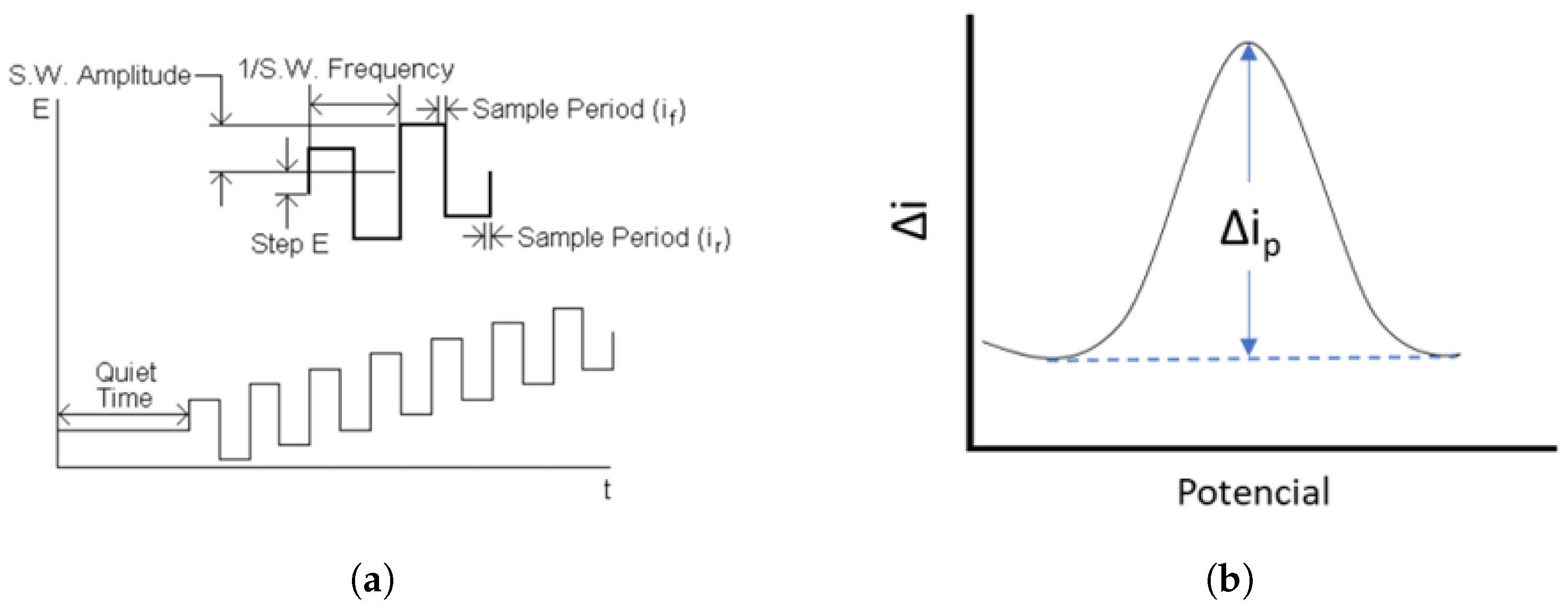
This experiment consisted of using square wave voltammetry (SWV) to determine the amount of nitrite present in three samples, one generated from a sausage, one from cold cuts, and one from ham. The SWV technique involves a square wave mounted over an offset that is increasing at a specific voltage step each cycle, this generates a “current peak” response at a specific potential value which in this case will be the current needed to oxidize the nitrites and the potential at where this oxidation occurs.
Figure 20 shows the voltage applied and a typical expected current response.
The nitrite content in the meat products was initially assessed using the AOAC (1997) method [
28], which is based on the classical Griess–Ilosvay technique. In this recognized method, nitrite undergoes diazotization with sulfanilic acid. Subsequently, it reacts with
-naphthylamine hydrochloride in an acidic medium (pH 2.5–5.0) to produce a pink azo dye (
-naphthylamino-p-azobenzeno-p-sulfonic acid). The absorbance of this dye at 520 nm directly correlates with nitrite concentration.
In the present study, the same AOAC sample preparation protocol was employed; however, detection was conducted utilizing a voltammetric system developed specifically for this work. Detection was achieved using a carbon paste electrode (CPE) as the working electrode, an Ag/AgCl reference electrode, and a platinum auxiliary electrode. The optimized electrochemical parameters included a supporting electrolyte of 0.1 mol acetate buffer at pH 3.3, with detection via square wave voltammetry (SWV) within a potential window of 0.6 to 1.3 V. The SWV parameters were set to 50 Hz, a step increment of 10 mV, and an amplitude of 75 mV. A scan-rate study revealed that the oxidation of nitrite on the CPE surface is predominantly diffusion-limited.
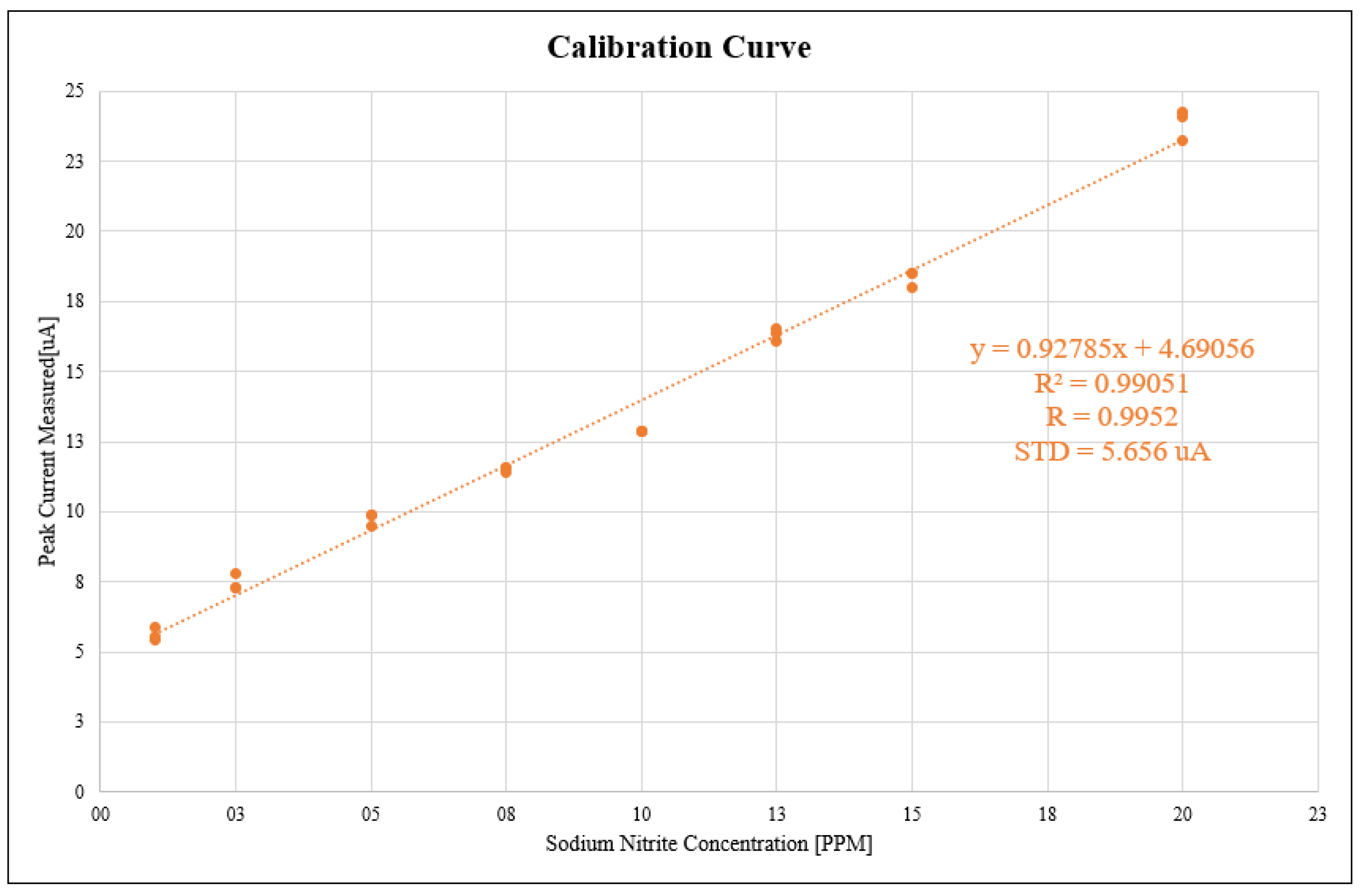
Previous to these measures, a calibration curve has to be made, this is normally achieved using pattern solutions whose concentrations are well known. This way, a proper relation between the current the instrument measures inside the electrochemical cell and the concentration of the analyte of interest can be established. To build the calibration curve, standard solutions of sodium nitrite (
) were prepared in acetate buffer at pH 3.3 across the concentration range of 1.0 to 20.0 ppm, utilizing ultra-pure water to prevent contamination. One at a time, the solutions with different concentrations were measured and the peak currents were registered. This way a calibration curve could be generated as shown in
Figure 21. Coefficients R,
and the standard deviation (STD), which are visible in the figure, result R = 0.9952,
= 0.9905 and STD = 5.656 µA. The linear regression equation for the calibration curve is described in equation [
8].
It is important to also mention that three samples for each concentration step were taken, with the intention to perform an analysis of variance (ANOVA) and evaluate the reproducibility of the method and precision of the instrument. Due to the calibration curve, these experiments and determinations are independent from the current response of the instrument, of course, the current response of the instrument will dictate the detection limit. On this occasion, the instrument is measuring currents from 5.42 µA up to 24.2 µA and is capable of detecting concentrations from 1 ppm up to 20 ppm.
For the analysis of real samples, 10 g of each homogenized sausage, cold-cut sausage, and ham were dispersed in 50 mL of hot ultra-pure water (50 °C). Subsequently, 5 mL of 5% (
w/
v) borax solution was added, and the mixture was maintained in a water bath for 15 min under continuous stirring. After cooling to ambient temperature, 5 mL of 0.270 mol
potassium ferrocyanide (
) and 5 mL of 1 mol
zinc sulfate (
) were incorporated with additional stirring for 5 min. The mixture was then transferred to a 100 mL volumetric flask, allowed to stand for 30 min, and its volume was adjusted to the mark with ultra-pure water, followed by stirring for an additional 15 min. Following the formation of a yellow precipitate, the supernatant was filtered and analyzed according to the AOAC (1997) protocol [
28] for nitrite in cured meats, using our voltammetric detection system instead of the traditional colorimetric method.
Square wave signals were generated with the developed potentiostat, and the nitrite oxidation peak currents were recorded and correlated with concentration using the calibration curve constructed from
standard solutions. The ANOVA performed demonstrated that the regression model was highly significant (
), with a non-significant lack-of-fit test (
), thereby confirming the statistical validity of the calibration. Predictions of independent real samples exhibited excellent reproducibility, with variations below 0.1% between replicates (three replicates were perform for each sample;
n = 3). This indicates that the proposed method and portable system yield precise and reliable nitrite determinations in sausage, cold-cut sausage, and ham, even at low concentration levels. The results obtained for the real samples are displayed in
Table 5.
The comparison between the proposed voltammetric method and the reference method (AOAC, modified Griess method) was performed using a paired t-test (n = 3, = 0.05). The differences in the concentrations obtained by the two techniques showed a mean difference of −0.01 ppm and a standard deviation of 0.48 ppm. The calculated t-value was |0.04|, which is smaller in magnitude than the critical value ( for , ). As a result, no statistically significant difference was observed at the 95% confidence level, confirming agreement between the proposed and reference methods for nitrite determination in the analyzed samples.
7. Results and Discussion
As discussed throughout this work, the primary limitations of the developed equipment stem from the selected ADC and the noise isolation. Currently, these factors restrict stable operation to the range of a few hundred nanoamperes, particularly during square wave voltammetry (SWV), which is the technique most sensitive to noise. However, the analog front-end (AFE) is capable of resolving currents as low as 1 nA; consequently, further testing is warranted to explore the lower limits of this architecture.
Regarding theoretical sensitivity, the detection limits for SWV are typically between 20 and 100 ppb, and can reach as low as 0.1–1 ppb when coupled with pre-concentration steps (stripping voltammetry) [
29]. In contrast, cyclic voltammetry (CV) has a much higher detection limit, generally in the range of 2000–10,000 ppb due to the capacitive charging current [
30].
From an instrumental perspective, the limit of detection (LOD) depends on the lowest current signal the device can reliably measure. However, the generation of this current is governed by the electrochemical system itself: the electrolyte, the analyte concentration, the optimization of experimental parameters, and strictly, the material and surface condition (polishing) of the electrodes.
In the validation case study presented here (nitrite determination), a 1 ppm sodium nitrite standard solution yielded a current response of 5.42 µA. This represents a relatively large signal for the instrument, indicating it is operating well above its noise floor at this concentration. Therefore, to fully characterize the ultimate detection limits of both the instrument and the implemented techniques, further experimentation at lower concentrations is required.
7.1. Noise Contribution
In the nanoampere measurement range, the 50 Hz noise component becomes a dominant factor, contributing errors of approximately ±50 nA per sample. This interference, compounded by the ADC’s limited sampling rate and lack of inherent 50 Hz rejection, effectively defines the system’s detection limit; furthermore, the low sampling rate precludes the use of digital post-processing filters to remove this noise. However, the sensitivity of the analog front-end was validated independently of the ADC: currents between ±68.2 nA were successfully resolved using a 30 M dummy load and direct oscilloscope monitoring.
7.2. Application Fields of the Developed Device
Recent studies document incidents of fraud and adulteration in meat products [
31,
32]. Therefore, the implementation of portable electrochemical analyzers represents an effective strategy to improve surveillance, reduce health risks, and protect consumers, as they offer rapid and quantitative results that facilitate preliminary screening before sending samples to a laboratory [
33].
Although the device was initially tested for nitrite determination, it is suitable for both inorganic and organic analysis. Voltammetric techniques are standard for determining inorganic analytes such as Pb, Cd, Cu, Fe, and Zn in various oxidation states. However, organic compounds can also be determined if they possess electroactive functional groups. Examples include pharmaceuticals like paracetamol, biomolecules like glucose, and compounds such as caffeine or polyphenols. For these organic applications, chemically modified electrodes are frequently required to achieve proper sensitivity.
The results presented in this work demonstrate that this device is suitable for use both as a screening tool and as a functional instrument for the quantitative analysis of selected analytes, within the discussed operational limitations. However, further analysis and comparison with commercial instrumentation remain advisable.
7.3. Improvement Potential
The developed system presents a solid foundation for future iterations that could significantly increase its analytical precision and versatility. From a hardware perspective, performance could be substantially enhanced by upgrading the analog-to-digital converter (ADC) to a higher-specification model, such as the ADS1255. This upgrade would not only provide a faster sampling rate but also offer inherent 50 Hz noise rejection, a critical feature for low-current measurements. Additionally, signal integrity could be further fortified by implementing superior electromagnetic shielding, within a grounded Faraday cage. On the software front, the repertoire of available voltammetric techniques could be expanded.
Furthermore, to achieve true scalability, a dedicated API could be developed. This would empower users to script and integrate their own custom voltammetric sequences directly into the software, potentially transforming the device into a fully open and customizable research platform.
8. Conclusions
As a result of the research, an instrument with good performance, linear behavior, and acceptable precision was developed. This was feasible and viable, allowing the reduction in a large and expensive desktop equipment to a lightweight, small, reliable, field-useful, and inexpensive portable equipment.
The idea of manufacturing a single device with software-scalable capabilities is feasible, allowing for further expansion through updates. Furthermore, when compared to commercial equipment, the results were very positive, with minor differences due to the components used. The result was a fully functional device capable of measuring the electrochemical currents produced in the cell with high precision and representing this information graphically.
In addition to performing electrical tests, the quality and analytical response of the equipment could be validated through the detection and quantification of nitrite in food samples.
Supplementary Materials
The following supporting information can be downloaded at:
https://www.mdpi.com/article/10.3390/hardware3040017/s1, CAD file S1: ProPrj_Potentiostat.epro; Gerber files: Gerber_PCB_design.zip; CSV file: BOM_potentiostat.csv; STL file S1: Box.stl; STL file S2: Box_cover.stl; CAD file S2: Case.f3d; Software: interface.py; Firmware S1: ADC_Library; Firmware S2: DAC_Library; Firmware S3: Config_Library; Firmware S4: Timer_Library.
| Name | Type | Description |
| S1 | CAD file | EasyEDA project - PCB design and schematics |
| S2 | Gerber files | .zip with PCB manufacturing files |
| S3 | CSV file | Bill of materials for PCB assembly |
| S4 | STL file | 3D Printing Designs |
| S5 | STL file | 3D Printing Designs |
| S6 | CAD file | Fusion360 project |
| S7 | Software | Script for GUI |
| S8 | Firmware | ADC control library in C |
| S9 | Firmware | DAC control library in C |
| S10 | Firmware | System setup library in C |
| S11 | Firmware | Timers control library in C |
Author Contributions
Conceptualization, D.A.C.G., R.B.P., D.D.d.S.F., R.M.S., and G.E.; methodology, D.A.C.G., D.D.d.S.F. and G.E.; software, D.A.C.G. and R.B.P.; validation, D.A.C.G., R.B.P. and D.D.d.S.F.; formal analysis, D.A.C.G., R.B.P., D.D.d.S.F. and G.E.; investigation, D.A.C.G., R.B.P., D.D.d.S.F. and G.E.; writing—original draft preparation, D.A.C.G. and R.B.P.; writing—review and editing, D.D.d.S.F., R.M.S. and G.E.; visualization, D.A.C.G., R.B.P., and G.E.; supervision, D.D.d.S.F., R.M.S. and G.E.; project administration, G.E. All authors have read and agreed to the published version of the manuscript.
Funding
This research received no external funding.
Institutional Review Board Statement
Not applicable.
Informed Consent Statement
Not applicable.
Data Availability Statement
Acknowledgments
The authors thank the INQUISUR and Chemistry Department Laboratories (Universidad Nacional del Sur, Bahía Blanca, Buenos Aires, Argentina) for providing us with the facilities to test our prototype.
Conflicts of Interest
The authors declare no conflicts of interest.
Appendix A. Feedback Capacitors and Maximum Scale Current Calculations
Appendix A.1. Maximum Scale Currents
To calculate the maximum current values that the transimpedance amplifier scales can handle, Equation (
A1) was used.
Taking into account the system operative range from −2.048 V to 2.048 V and replacing with the chosen feedback resistors values, it is possible to obtain the maximum current that the transimpedance amplifier can handle for that feedback resistor or scale.
The resistors were calculated previously using Equation (
A1) and a desired current value; once these resistors’ values were obtained, they were replaced with their closest commercial resistor value and currents were recalculated with it.
So, for every feedback resistor value or “instrument scale”:
Appendix A.2. Feedback Capacitors
For the calculations of the feedback capacitors, Equation (
3) was used, with an operation frequency of 1 kHz and the appropriate feedback resistor value for each gain scale. The calculations will be displayed next:
Appendix B. Schematics
The following images that are shown on the following pages are the schematic circuits of the instrument and are own authorship.
References
- Overton, E.B.; Dharmasena, H.; Ehrmann, U.; Carney, K.R. Trends and advances in portable analytical instrumentation. Field Anal. Chem. Technol. 1996, 1, 87–92. [Google Scholar] [CrossRef]
- Duan, C.; Li, J.; Zhang, Y.; Ding, K.; Geng, X.; Guan, Y. Portable instruments for on-site analysis of environmental samples. TrAC Trends Anal. Chem. 2022, 154, 116653. [Google Scholar] [CrossRef]
- Jornet-Martínez, N.; Moliner-Martínez, Y.; Molins-Legua, C.; Campíns-Falcó, P. Trends for the Development of In Situ Analysis Devices. In Encyclopedia of Analytical Chemistry; John Wiley & Sons, Ltd.: Hoboken, NJ, USA, 2017; pp. 1–23. [Google Scholar] [CrossRef]
- Zhang, C. Fundamentals of Environmental Sampling and Analysis, 1st ed.; John Wiley & Sons, Inc.: Hoboken, NJ, USA, 2007; Chapter 11; pp. 289–308. ISBN 978-0-471-71097-4. [Google Scholar]
- Vasilescu, A.; Hayat, A.; Gáspár, S.; Marty, J.L. Advantages of Carbon Nanomaterials in Electrochemical Aptasensors for Food Analysis. Electroanalysis 2018, 30, 2–19. [Google Scholar] [CrossRef]
- Ren, H.; Wei, T. Electrochemical Synthesis Methods of Metal-Organic Frameworks and Their Environmental Analysis Applications: A Review. ChemElectroChem 2022, 9, e202200196. [Google Scholar] [CrossRef]
- Pi, R. Raspberry Pi Hardware. Available online: https://www.raspberrypi.com/documentation/computers/raspberry-pi.html#introduction (accessed on 25 November 2025).
- Dryden, M.D.M.; Wheeler, A.R. DStat: A Versatile, Open-Source Potentiostat for Electroanalysis and Integration. PLoS ONE 2015, 10, e0140349. [Google Scholar] [CrossRef] [PubMed]
- Paul Grohe, T.I. Design fEmtoampere Circuits with Low Leakage, Part 2: Component Selection. 2012. Available online: https://www.edn.com/design-femtoampere-circuits-with-low-leakage-part-2-component-selection/ (accessed on 25 November 2025).
- Paul Grohe, T.I. Design Femtoampere Circuits with Low Leakage, Part 3: Low-Current Design Techniques. 2012. Available online: https://www.edn.com/design-femtoampere-circuits-with-low-leakage-part-3-low-current-design-techniques/ (accessed on 25 November 2025).
- Texas Instruments, Inc. LMP770X Precision, CMOS Input, RRIO, Wide Supply Range Amplifiers. Available online: https://www.ti.com/lit/ds/symlink/lmp7702.pdf?ts=1750631870926 (accessed on 25 November 2025).
- Texas Instruments, Inc. OPA322: 20-MHz, Low-Noise, 1.8-V, RRI/O, CMOS Operational Amplifier With Shutdown. Available online: https://www.ti.com/lit/ds/symlink/opa322.pdf?ts=1750700309054 (accessed on 25 November 2025).
- Texas Instruments, Inc. OPA320: Precision, 20-MHz, 0.9-pA, Low-Noise, RRIO, CMOS Operational Amplifier With Shutdown. Available online: https://www.ti.com/lit/ds/symlink/opa320.pdf?ts=1750667933119 (accessed on 25 November 2025).
- Texas Instruments, Inc. LMP7721 3-Femtoampere Input Bias Current Precision Amplifier. Available online: https://www.ti.com/lit/ds/symlink/lmp7721.pdf?ts=1764089686281&ref_url=https%253A%252F%252Fwww.ti.com%252Fproduct%252Fes-mx%252FLMP7721 (accessed on 25 November 2025).
- Grohe, P. LMP7721 Multi-Function Evaluation Board Users’ Guide. Natl. Semicond. 2010, 1. Available online: https://www.ti.com/lit/ug/snou004/snou004.pdf (accessed on 7 December 2025).
- Rich, A. Shielding and Guarding: How to Exclude Interference-Type Noise. Application Note AN-347, Analog Devices, 1983. Originally published in Analog Dialogue 17-1. Available online: https://www.analog.com/media/en/technical-documentation/application-notes/41727248AN_347.pdf (accessed on 25 November 2025).
- Keithley Instruments, Inc. Low Level Measurements Handbook: Precision DC Current, Voltage, and Resistance Measurements, 7th ed.; Keithley Instruments, Inc.: Cleveland, OH, USA, 2013; See Section 2.3.1: Guarding. [Google Scholar]
- Analog Devices, Inc. High-Speed, Low-Voltage, CMOS Analog Multiplexers/Switches. Available online: https://www.analog.com/media/en/technical-documentation/data-sheets/MAX4617-MAX4619.pdf (accessed on 25 November 2025).
- Analog Devices, Inc. 14-/16-Bit, Low-Power, Buffered Output, Rail-to-Rail DACs with I2C Interface. Available online: https://www.analog.com/media/en/technical-documentation/data-sheets/MAX5215-MAX5217.pdf (accessed on 25 November 2025).
- The MathWorks, Inc. Fourth-Order Sallen-Key Lowpass Filter. Available online: https://la.mathworks.com/help/sps/ug/fourth-order-sallen-key-lowpass-filter.html (accessed on 25 November 2025).
- Analog Devices, Inc. SOT23, Low-Noise, Low-Distortion, Wide-Band, Rail-to-Rail Op Amps. Available online: https://www.analog.com/media/en/technical-documentation/data-sheets/MAX4475-MAX4489.pdf (accessed on 25 November 2025).
- Texas Instruments, Inc. 16-Bit ANALOG-TO-DIGITAL CONVERTER with Onboard Reference. Available online: https://www.ti.com/lit/ds/symlink/ads1110.pdf (accessed on 25 November 2025).
- Texas Instruments, Inc. LM4040 Precision Micropower Shunt Voltage Reference. Available online: https://www.ti.com/lit/ds/symlink/lm4040.pdf?ts=1750679438094 (accessed on 25 November 2025).
- EasyEDA. Available online: https://easyeda.com/page/download (accessed on 25 November 2025).
- Autodesk, Inc. Available online: https://www.autodesk.com/education/edu-software/fusion (accessed on 25 November 2025).
- Bioanalytical Systems, Inc. Instruction Manual for BAS Epsilon Electrochemistry; 2005. Version 2.10.73. Available online: https://www.basinc.com/assets/library/manuals/EC_epsilon/EC_epsilon_Manual.pdf (accessed on 7 December 2025).
- Krepper, G. Desarrollo de Nuevos MéTodos AnalíTicos para la Determinación de Contaminantes en Productos Apícolas: Empleo de Sistemas Electroquímicos. Ph.D. Thesis, Universidad Nacional del Sur, Bahía Blanca, Argentina, 2018. [Google Scholar]
- Association of Official Analytical Chemists. Official Methods of Analysis of the Association of Official Analytical Chemists, 16th ed.; AOAC International: Gaithersburg, MD, USA, 1997; Method 982.22. [Google Scholar]
- Wang, J. Analytical Electrochemistry, 3rd ed.; Wiley-VCH: Hoboken, NJ, USA, 2006. [Google Scholar]
- Bard, A.J.; Faulkner, L.R. Electrochemical Methods: Fundamentals and Applications, 2nd ed.; John Wiley & Sons: New York, NY, USA, 2001. [Google Scholar]
- European Commission. Overview Report—Fighting Fraudulent Practices in the Agri-food Chain; Technical report; European Commission: Brussels, Belgium, 2023. [Google Scholar]
- Ventura, S.F.; de Freitas, W.A.; Duarte, M.T.; da Silva, A.C.F.; de Fátima Carrijo, K. Nitrito residual em salsichas comercializadas no Brasil procedentes de indústrias fiscalizadas pelo Serviço de Inspeç ao Federal. Braz. J. Vet. Med. 2017, 39, 111–114. [Google Scholar] [CrossRef]
- Ferrari, A.G.M.; Crapnell, R.D.; Banks, C.E. Electrochemical Sensing Platforms for Food and Drink Safety. Biosensors 2021, 11, 291. [Google Scholar] [CrossRef] [PubMed]
Figure 1.
System block diagram.
Figure 1.
System block diagram.
Figure 2.
Simplified implemented circuit for potential injection for CE and feedback through RE.
Figure 2.
Simplified implemented circuit for potential injection for CE and feedback through RE.
Figure 3.
Implemented circuit for potential injection for CE and feedback through RE with real components.
Figure 3.
Implemented circuit for potential injection for CE and feedback through RE with real components.
Figure 4.
Transimpedance-amplifier-simplified circuit with driven shield.
Figure 4.
Transimpedance-amplifier-simplified circuit with driven shield.
Figure 5.
Gain selector circuit. Gains are represented as blocks for simplicity. Selector is represented as a plain selector switch to conceptualize the idea.
Figure 5.
Gain selector circuit. Gains are represented as blocks for simplicity. Selector is represented as a plain selector switch to conceptualize the idea.
Figure 6.
Antialiasing filter topology. This filter is implemented after the DAC to soften the output signal and prevent glitches.
Figure 6.
Antialiasing filter topology. This filter is implemented after the DAC to soften the output signal and prevent glitches.
Figure 7.
Block diagram illustrating ADC place in the system.
Figure 7.
Block diagram illustrating ADC place in the system.
Figure 8.
Data communication flow between GUI and firmware diagram. The yellow charts denote processes executed by the GUI, whereas the blue charts indicate firmware execution.
Figure 8.
Data communication flow between GUI and firmware diagram. The yellow charts denote processes executed by the GUI, whereas the blue charts indicate firmware execution.
Figure 9.
Main user graphic interface screen.
Figure 9.
Main user graphic interface screen.
Figure 10.
PCB final design.
Figure 10.
PCB final design.
Figure 11.
(A) Final PCB after soldering all components. (B) Lab-made stencil used.
Figure 11.
(A) Final PCB after soldering all components. (B) Lab-made stencil used.
Figure 12.
The whole case design renders can be explore in this figure: (a) Empty case exterior and interior visualization. (b) Rotated case visualization with Raspberry, the potentiostat PCB and a BNC connector mounted in the case. (c) Case front view with some mounted components. (d) Case cover design.
Figure 13.
Instrument final design implemented.
Figure 13.
Instrument final design implemented.
Figure 14.
Parameters validation message boxes.
Figure 14.
Parameters validation message boxes.
Figure 15.
Graphical data visualization.
Figure 15.
Graphical data visualization.
Figure 16.
File drop down menu: Save File window.
Figure 16.
File drop down menu: Save File window.
Figure 17.
Linearity comparison between lab-made potentiostat and commercial equipment (Epsilon). Orange curve represents the lab-made equipment response, meanwhile the blue curve represents the commercial equipment response; shadings represents standard deviation. The linear regressions equations for each curve and their R2 coefficients are also visible in the graphic.
Figure 18.
Linearity experiments with dummy cells. Potentiostat GUI screenshots. (A) Dummy cell with 1 M resistor. (B) Dummy cell with 30 M resistor.
Figure 18.
Linearity experiments with dummy cells. Potentiostat GUI screenshots. (A) Dummy cell with 1 M resistor. (B) Dummy cell with 30 M resistor.
Figure 19.
Pattern solutions mean voltammograms using cyclic voltammetry technique. Orange curve represents the lab-made equipment response, meanwhile the blue curve represents the Commercial equipment response. Each color shading represents the standard deviation for each curve.
Figure 19.
Pattern solutions mean voltammograms using cyclic voltammetry technique. Orange curve represents the lab-made equipment response, meanwhile the blue curve represents the Commercial equipment response. Each color shading represents the standard deviation for each curve.
Figure 20.
Square wave voltammetry technique. (
a) Applied potential and its adjustable parameters [
26]. (
b) Square wave voltammetry typical expected current response [
27].
Figure 20.
Square wave voltammetry technique. (
a) Applied potential and its adjustable parameters [
26]. (
b) Square wave voltammetry typical expected current response [
27].
Figure 21.
Sodium nitrite calibration curve.
Figure 21.
Sodium nitrite calibration curve.
Table 1.
This table contains a general list of materials needed for the build process.
Table 1.
This table contains a general list of materials needed for the build process.
| Quantity | Component | Source | Cost [USD] |
|---|
| 1 | Raspberry Pi 3B+ | Amazon | 47.90 |
| 3 | BNC Straight Bulkhead 50 Ohm | Digikey | 1.46 |
| 1 | PCB | JLC PCB | 2.00 |
| 1 | Electronic Components | LCSC Electronics | 30.55 |
Table 2.
Bill of materials.
Table 2.
Bill of materials.
| Quantity | Component | Designator | Value | Unit Cost [USD] |
|---|
| 11 | SMD Capacitor | C1, C2, C3, C4,
C5, C13, C15, C20,
C21, C22, C24 | 100n | USD 0.007 |
| 2 | SMD Capacitor | C6 | 5.6p | USD 0.0014 |
| 1 | SMD Capacitor | C7 | 6.8p | USD 0.0014 |
| 2 | SMD Capacitor | C8, C18 | 68p | USD 0.005 |
| 1 | SMD Capacitor | C9 | 680p | USD 0.005 |
| 1 | SMD Capacitor | C10 | 4.7n | USD 0.0014 |
| 1 | SMD Capacitor | C11 | 56n | USD 0.007 |
| 1 | SMD Capacitor | C12 | 1u | USD 0.0042 |
| 3 | SMD Capacitor | C14, C23, C25 | 100p | USD 0.0032 |
| 2 | SMD Capacitor | C16, C17 | 180p | USD 0.0051 |
| 1 | SMD Capacitor | C19 | 160p | USD 0.0038 |
| 1 | SMD Capacitor | C26 | 10n | USD 0.0033 |
| 1 | SMD Resistor | R1 | 100M | USD 0.0086 |
| 1 | SMD Resistor | R2 | 30M | USD 0.0014 |
| 1 | SMD Resistor | R3 | 3M | USD 0.0014 |
| 1 | SMD Resistor | R4 | 330k | USD 0.0019 |
| 1 | SMD Resistor | R5 | 33k | USD 0.001 |
| 2 | SMD Resistor | R14, R15 | 25.5k | USD 0.0009 |
| 2 | SMD Resistor | R18, R19 | 18.7k | USD 0.0011 |
| 5 | SMD Resistor | R8, R9, R20,
R21, R22 | 10k | USD 0.0008 |
| 1 | SMD Resistor | R6 | 3.3k | USD 0.001 |
| 4 | SMD Resistor | R16, R17,
R23, R24 | 1k | USD 0.0005 |
| 5 | SMD Resistor | R7, R10, R11,
R28, R29 | 100 | USD 0.0018 |
| 1 | Header-Male-2.54 | H_CE | 1 × 1 | USD 0.001 |
| 2 | Header-Male-2.54 | H_REF, H_WRK | 1 × 2 | USD 0.0035 |
| 1 | Header-Female-2.54 | PI-HEADER | 2 × 20 | USD 0.0298 |
| 1 | Precision Op Amp | U1 | LMP7721MA | USD 3.003 |
| 1 | Analog Multiplexer | U2 | MAX4617CSE | USD 3.096 |
| 1 | Precision Op Amp | U3 | LMP7702MA | USD 3.6825 |
| 1 | Precision Op Amp | U4, U5 | LMP7701MF | USD 2.55 |
| 1 | 16 bits ADC | U6 | ADS1110A0IDBVR | USD 1.0245 |
| 1 | 16 bits DAC | U7 | MAX5217BGUA | USD 8.89 |
| 1 | Precision Op Amp | U8 | MAX4477ASA | USD 3.81 |
| 1 | Precision shunt Vref | U9 | LM4040-4.1 | USD 0.882 |
| 1 | Precision shunt Vref | U10 | LM4040-2.0 | USD 0.85 |
Table 3.
This table contains the Dummy Cells Resistors used to test and a specific current scale.
Table 3.
This table contains the Dummy Cells Resistors used to test and a specific current scale.
| Dummy Cell Test Resistor | Target Scale | N° of Replicates |
|---|
| 120 M | 1 nA and 40 nA | 5 |
| 30 M | 100 nA | 5 |
| 10M | 1 µA | 5 |
| 1 M | 10 µA | 5 |
| 100 k | 100 µA | 5 |
| 4.7 k | 1 mA | 5 |
| 1 k | 10 mA | 5 |
| 220 | 40 mA | 5 |
Table 4.
This table summarize the experimental solutions, temperature, concentrations, and number of replicates for each case.
Table 4.
This table summarize the experimental solutions, temperature, concentrations, and number of replicates for each case.
| Pattern Solution | Temperature | Concentration | N° of Replicates |
|---|
| 20 ºC | 7.5 mM | 5 |
| KCL | 20 ºC | 0.1 M | 5 |
Table 5.
This table contains the mean peak current measured, the obtained mean concentration with the proposed method and the the reference method, and the difference between both methods is expressed in percentage.
Table 5.
This table contains the mean peak current measured, the obtained mean concentration with the proposed method and the the reference method, and the difference between both methods is expressed in percentage.
| Sample | Peak Current Measured [µA] | Proposed Method [ppm] | Reference Method [ppm] | Difference [%] |
|---|
| Sausage | 13.1 | 9.20 | 9.50 | −3.16 |
| Cold-cut | 21.4 | 18.34 | 17.70 | 3.61 |
| Ham | 13.7 | 9.86 | 10.10 | −2.37 |
| Disclaimer/Publisher’s Note: The statements, opinions and data contained in all publications are solely those of the individual author(s) and contributor(s) and not of MDPI and/or the editor(s). MDPI and/or the editor(s) disclaim responsibility for any injury to people or property resulting from any ideas, methods, instructions or products referred to in the content. |
© 2025 by the authors. Licensee MDPI, Basel, Switzerland. This article is an open access article distributed under the terms and conditions of the Creative Commons Attribution (CC BY) license (https://creativecommons.org/licenses/by/4.0/).
