Article

Low-Voltage Control Circuits of Formula Student Electric Racing Cars

by
Ahmed Darwish Badawy
1,2,*,
Stefan Sfranciog
1,
Jorge Takeshi Hiranoyama
1,
Jaime Lacasta Ibarrola
1,
James Engstrom
1,
Kirollos Mikhail
1,
William Hunt
1,
Joshua Hartley
1,
Fatemeh Nasr Esfahani
1 and
Amos Dexter
1
1
School of Engineering, Lancaster University, Lancaster LA1 4YR, UK
2
Faculty of Engineering & Digital Technologies, University of Bradford, Bradford BD7 1AZ, UK
*
Author to whom correspondence should be addressed.
Hardware 2024, 2(3), 190-222; https://doi.org/10.3390/hardware2030010
Submission received: 27 April 2024 / Revised: 30 July 2024 / Accepted: 31 July 2024 / Published: 3 August 2024

Abstract

:
Formula Student (FS) competitions aim to prepare and encourage engineering students to participate in the progression of automotive and motorsport industries. The built racing cars adhere to strict regulations set by competition guidelines to ensure the safety of both teams and spectators. For electric racing cars, the high-voltage (HV) battery system usually operates within a voltage range between 100 V to 600 V to supply the motor and its controller with the required electrical power. It is essential to ensure that these components are operating effectively to minimize battery and motor current as well as to ensure efficient and reliable performance throughout the race. A low-voltage control system (LVCS), usually operating at 12 V, is used to coordinate a wide array of critical operational and safety functions to control the HV system. These functions include: (1) turning on/off procedures, (2) monitoring speed, voltage, and current, (3) interfacing with pedals, (4) controlling dashboard features, (5) managing lighting, (6) facilitating data communication, and (7) implementing safety protocols. The design and operation of the LVCS are crucial for compliance with safety regulations and enhancing the FS electric racing car (FSERC) performance. This details and discusses the design procedures of the LVCS, using the Lancaster E-Racing (LER) FSERC as a case study. The LER car employs a 400 V battery system to power a 68-kW permanent manet synchronous motor (PMSM) using a three-phase voltage source inverter. Using mathematical analysis, SIMULINK/MATLAB® computer simulations, and the experimental real-data results provided by the LER FSERC, this study seeks to offer valuable insights regarding the LVCS practical implementation and optimization.

1. Introduction

Driven by the international desire to electrify transportation, there has been a notable surge in the number of electric racing cars participating in Formula Student (FS) competitions worldwide. As a part of their degree-level project, engineering students in different universities participate in the FS competition which supports them in transition from university studies to automotive and motorsport sectors. Thus, the project is backed and sponsored by industry to provide the newly graduate engineers with practical engineering experience as well as softs skills especially project management. In the UK, specifically in the FSUK competition managed by the Institution of Mechanical Engineers (IMechE), electric cars formed more than two-thirds of the participant vehicles in 2023, with this figure anticipated to rise in subsequent years [1,2,3,4]. This trend is not only driven by the economic and environmental advantages of electric racing cars but also by their exceptional dynamic performance characteristics, including torque, speed, and power, which surpass those of traditional petrol racing cars [1,2,3,4].
Formula Student electric racing cars (FSERCs) are powered by electrical energy derived from a primary power source typically composed of series and parallel configurations of lithium-ion (Li-ion) battery cells [5,6]. The fundamental electrical components of an FSERC are illustrated in Figure 1 including:
  • The accumulator: This comprises the battery cells, high-voltage (HV) cables, protection devices, and the battery management system (BMS) which is responsible for monitoring and managing the batteries. Typically, the accumulator voltage is in the range of 100 V to 600 V based on the designed value of the DC-link voltage and hence the nominal voltage of the selected motor and its controller.
  • The motor controller (traction inverter): Typically, this component is a DC-AC inverter for AC motors or a DC-DC chopper for DC motors.
  • The electric motor: In the 2023 FSUK, all FSERCs utilized AC machines, either synchronous or induction. AC machines are favoured for their enhanced efficiency, compact size, higher power density, and the absence of carbon brushes, which require servicing every six months of operation [6]. Brushless DC (BLDC) motors utilize permanent magnet synchronous machines (PMSM) to generate a trapezoidal-shaped AC back electromotive force (EMF), which simplifies the modulation of the motor controller.
  • The HV system: This system encompasses the HV cables situated outside the accumulator, along with the protection fuses and the HV disconnect (HVD) interlocks. Its primary function is to manage the connection, disconnection, and safeguarding of electric current flow from the accumulator to the motor through the motor controller. It includes all components connected to the motor, inverter, the accumulator, and the DC-link between them.
  • The low-voltage (LV) system: This comprises the electronic system responsible for operating and controlling the HV systems within the FSERC. It usually operates at low voltage (LV) levels ranging from 6V to 24 V, with 12 V being a common value. The LV control system (LVCS) consists of various electronic circuits (ECs) assigned to different functions within the FSERC. These ECs are distributed across nearly every subsystem to fulfil a range of tasks, including toggling operations on/off, issuing warnings, transmitting data, or executing safety routines.
Comprehensive analyses and design methodologies relevant to FS competitions have been presented in [7,8,9,10]. The hardware and software components essential for developing a competitive FSERC are covered in [7]. The work discusses the selection of microcontrollers, analog signal acquisition circuits, and the design of a bespoke BMS and safety electronics, all of which are crucial for complying with competition rules. Additionally, the report introduces a modular software architecture that leverages an open-source bootloader for efficient firmware management and updates via a PC-hosted software tool, thereby enhancing the system’s flexibility and robustness. The distribution of inverters and the redesign of electronic components within the accumulator container are discussed in [8]. The report provides detailed insights into the electric powertrain and BMS, emphasizing their critical roles in optimizing vehicle performance and ensuring operational safety. The design and development of the motor controller (MC) for FS competition vehicles is provided in [10]. It details the various stages of MC development, introducing innovative methodologies for phase current sensing and control strategy improvements. These innovations aim to achieve simplicity, robustness, and cost-effectiveness. The thorough evaluation of the MC in laboratory settings ensures its readiness for integration into the vehicle, paving the way for future enhancements in control strategies and overall vehicle performance.
This paper outlines the design process of the ECs within the LVCS of the 2022 FSERC developed by the Lancaster E-Racing (LER) team. Additionally, the paper illustrates the operation of these ECs and discusses their impact on the FSREC’s performance. Section 2 provides a brief overview of the requirements and functions of each EC within the LVCS aided by mathematical analyses and computer simulations. Section 3 delves into the detailed configuration of individual ECs, elucidating the rationale behind their design. This section draws upon SIMULINK/MATLAB® R2024a software and experimental data to elucidate the ECs’ operation. Section 4 presents the real designs with listing the components employed to build and manufacture the ECs. In Section 5, experimental results from the FSERC constructed and designed by the LER team are presented to demonstrate the overall performance of the LVCS. Finally, Section 6 summarizes the main conclusions drawn from this work and suggests potential enhancements for the developed ECs.

2. Design Overview

The LVCS is designed to function at a voltage of 12 V and is powered by a low voltage battery (LVB). For this study, a 50 Ah LiFePO4 Lithium battery was selected as the LVB due to its remarkable durability, capable of enduring over 3000 cycles. Its high energy density and lightweight makes it an ideal choice for integration within the FSERC. The capacity of the battery is selected to endure the race period without exceeding a voltage of 1 V to ensure that the functionality of the LVCS is not affected. The next subsections will detail the primary components comprising the LVCS.

2.1. Shutdown Line

The shutdown (SD) line serves as the central component of the LVCS, facilitating the connection of LV power to various ECs via control switches and interlocks. Usually, the automotive connection relays have 12 V normally open (NO) coils and hence it is preferable to keep the SD line at the same voltage. Figure 2 shows the electrical connection of the ECs, switches, and interlocks as well as their physical locations in the FSERC chassis. The main purpose of the SD line is to ensure that all safety requirements are met before activating the HV system which means that battery voltage becomes present outside the accumulator. Beside the ECs to be presented in the following subsection, the components of the SD line are:
(a)
LV master switch (LVMS): this is an NO switch responsible for linking the LVB to the remainder of the line. The first EC connected to the SD line is the brake system plausibility device (BSPD), which will be presented alongside the other ECs in subsequent subsections.
(b)
SD switches: these are three normally closed (NC) manual emergency switches fitted in the cockpit, as well as on the right and left sides of the FSERC. The users can disconnect the SD line by pressing any of these three switches.
(c)
Inertia switch: this is an NC switch employed to safeguard the FSERC by detecting the sudden deceleration indicative of an accident and hence trip the SD line. The inertia switch is connected in series with the SD line following the three manual SD switches.
(d)
Brake over travel switch (BOTS): this is an NC switch located physically beyond the brake pedal and is used to trip the SD line when the driver exceeds the permissible range for pressing the pedal.
(e)
HVD interlock: this is a NC contact integrated within the HVD connector but electrically isolated from the HV path. The main function of the HVD interlock is to guarantee that the SD line is disconnected whenever the HVD plug is removed. This will ensure that the battery voltage will not be present at the terminals of the HVD if the plug is removed for any reason.
(f)
Tractive system master switch (TSMS): this NO manual switches should be the final connector in the SD line which will be switched on when the FSERC is ready to operate. Activating the TSMS signifies that the accumulator of the FSERC is prepared to be connected to the DC-link of the motor controller. The HV circuit will be closed by the activation logic (AL) EC which is responsible for turning the accumulator insulation relays (AIRs) on. It is worth noting that the negative terminal of the HV system is left floating while the ground of the LV system is connected to all conductive parts in the chassis.

2.2. BSPD Circuit

The main goal of the BSPD EC is to protect the electric motor from the danger of fires during hard braking when the driver tends to brake harshly during emergencies or cornering. A simple schematic for the motor connection is shown in Figure 3. The rms value of the motor current will increase significantly if the driver brakes the wheels when the MC is still generating three-phase voltage at the terminals of the PMSM stator. This leads the back emf to be lowered and the generated voltages will be subject to the low phase resistance and inductance in the motor circuit.
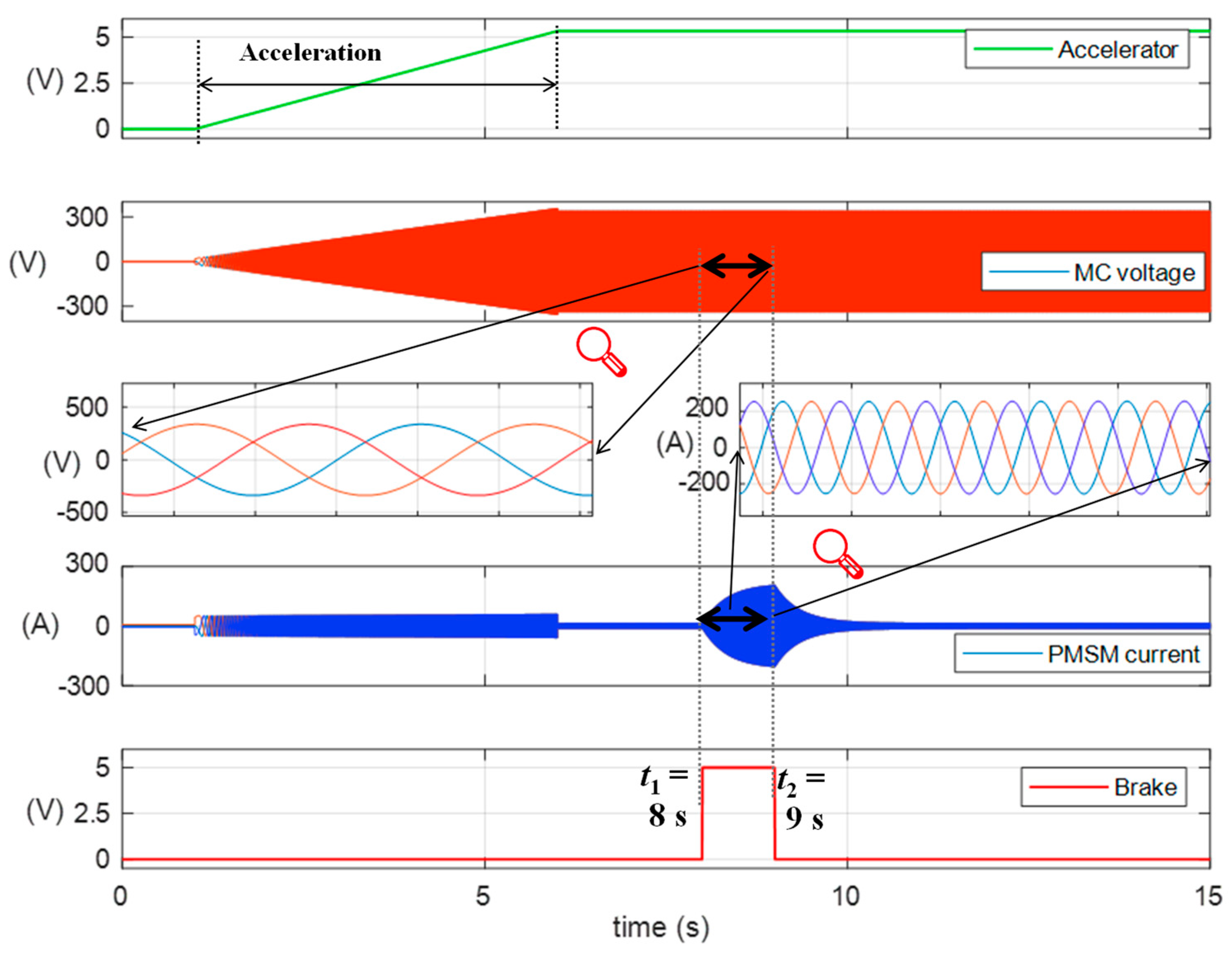
Figure 4 shows the SIMULINK/MATLAB simulation results for the FSERC drive system during hard braking with the parameters listed in Table 1. In the top graph, the driver increases the linear speed of the car using the accelerator pedal which transfers the 0–5 V analogue voltage command to the MC to control the output voltage and hence the motor’s speed. During the period 1 s to 6 s, the current of the PMSM is high in the range of 80 A to generate the high torque required for acceleration. Once the top speed is reached, the PMSM current follows the reduced torque and falls below 40 A. The 1-s period between t1 = 8s and t2 = 9 s shows the case when hard braking occurred without releasing the accelerator pedal. In this duration, the motor’s current increases to exceed the maximum permissible current for the system of 160 A which can cause a dangerous situation for the driver and other persons in the surrounding. Therefore, it is necessary and required by the safety rules that the overlap duration between the accelerator and brake pedals’ signals is reduced. The BSPD EC is designed to disconnect the DC-link of the HV system by tripping the AIRs if the overlap exceeds 500 ms. It is worth mentioning that the 500-ms duration is a guiding value and the exact value of the permissible overlap may be reduced further based on the calculations and the results obtained from the computer simulations or actual testing.
The PMSM model can be expressed as [11]:
V d V q = R s 0 0 R s I d I q + L d 0 0 L q d d t I d I q + ω 0 L q L d 0 I d I q + 0 λ
ω = P ω m
T e = 3 2 P λ I q ,
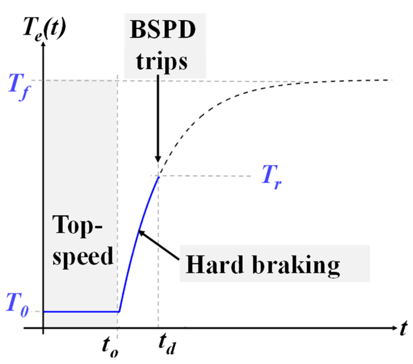
where Vd and Vq are the stator voltage expressed in the synchronous frame dq coordinates, Id and Iq are the stator dq currents, ω is the electrical frequency of the stator voltage, ωm is the rotational speed of the motor, λ is the flux linkage of the PMSM, Rs is the stator windings resistance, Ld and Lq are the dq components of the stator windings inductance, Te is the developed electromechanical torque and P is the number of pair of poles. Figure 5 shows the PMSM developed torque when the driver applies the full braking torque Tbr at the time instant t0. Prior to t0, the PMSM was controlled to generate the torque T0 which covers the load and friction torques which can be calculated from [12]:
T 0 = m g r µ r r + sin ψ G + 1 2 G 3 ρ A C d ω m 2 r 3 ,
where μrr, ψ, g, and ρ are the rolling resistance coefficient, the inclination of road surface, acceleration due to gravity, and density of air, respectively. The parameters m, G, A, Cd, and r also represent the vehicle mass, gearbox ratio, frontal area, drag coefficient, and wheel’s radius, respectively. As the racing track is usually flat, it can be considered that ψ = 0°. The PMSM developed torque continues to increase until the driver releases the brake pedal of the BSPD EC trips the TS system, whichever is sooner. If this did not occur and the system continued to operate at full voltage under hard braking, the developed torque will continue to increase until it reaches the maximum value Tf as:
Tf = T0 + Tbr
Accordingly, the maximum value of the PMSM q-axis current can be obtained from:
I q f = 2 T f 3 P λ
It can be seen from Figure 5 that adjusting the braking delay time td is critical to ensure that the PMSM torque does not exceed the permissible value Tr determined in the PMSM datasheet specifications.
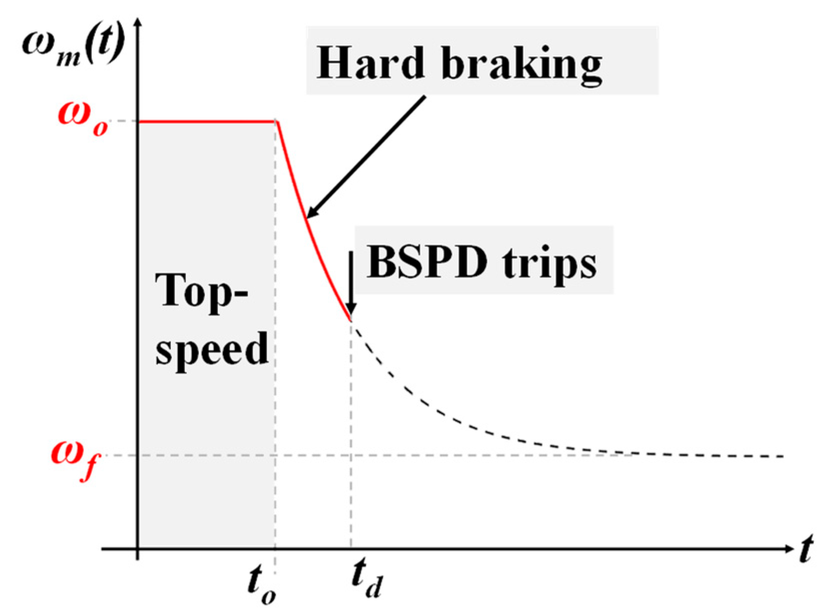
Meanwhile, the FSERC is decelerating and the speed of the PMSM is reducing as shown in Figure 6. The PMSM top speed at the instance of braking is calculated from:
ω 0 = v t o p r G ,
where vtop is the top linear speed of the car. The final speed of the PMSM ωf, which will be reached if the hard braking continues, can be calculated from (8). As the field-oriented control (FOC) is applied, Vq equals the peak value of the PMSM phase voltage.
ω f = R s P λ ± P λ 2 4 R I q f V q L q L d P 2 I q f R 2 L q L d P 2 I q f
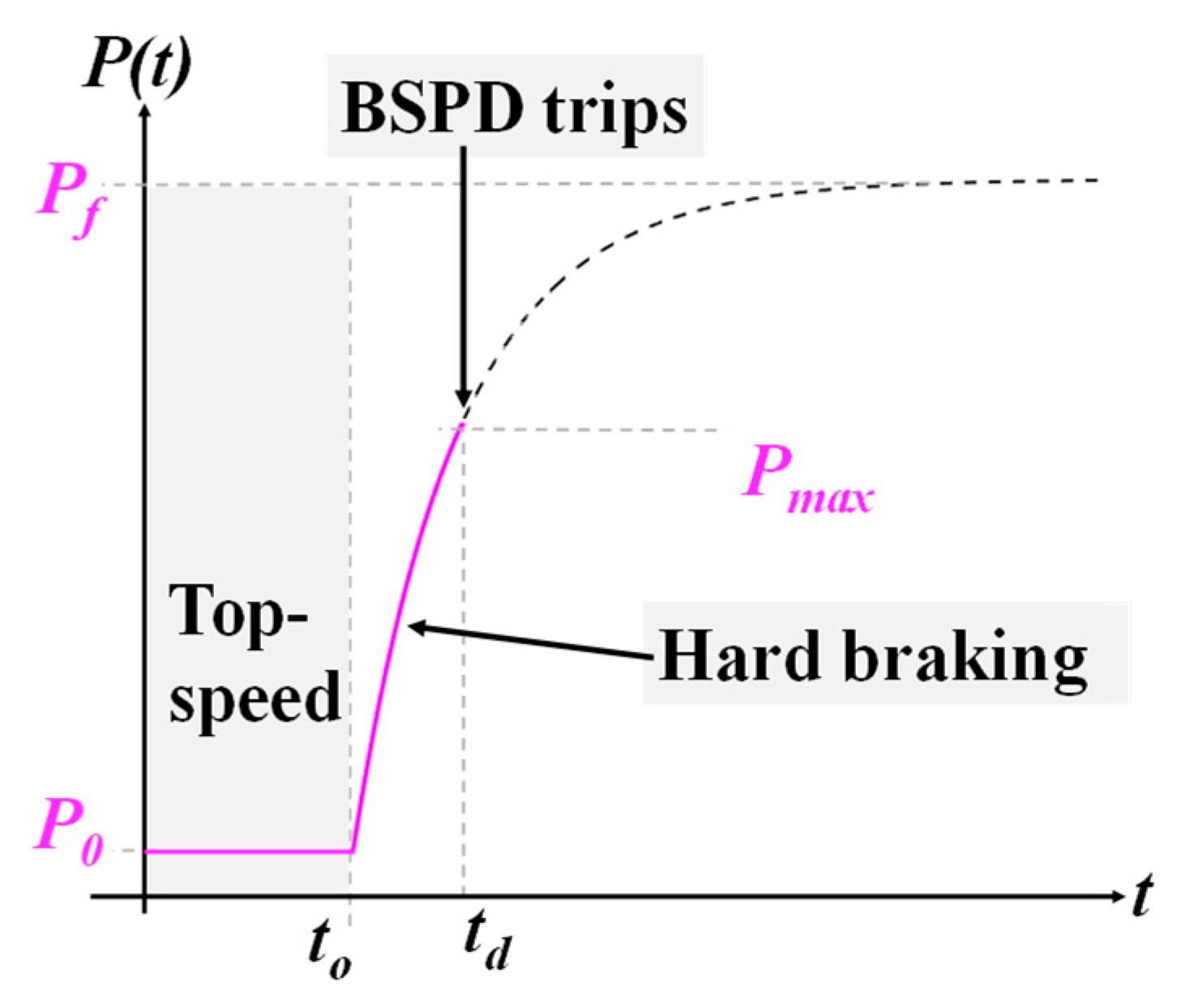
Figure 7 shows the power of the FSERC during braking from top speed. It is essential to ensure that the time delay td is designed by the BSPD EC, so the power does not exceed the peak instantaneous power of the full system Pmax either at the battery or the motor sides.
The instantaneous PMSM power is obtained from:
P t = T o + T b r ω f + T o + T b r ω o ω f T b r ω f e t τ T b r ω o ω f e 2 t τ ,  
where Jm and τ are the inertia and the time constant of the mechanical system and can be calculated from:
J m = m r 2 G 2
τ = J m ω o ω f T b r
Equations (9)–(11) are used to determine the delay td to trip the SD line when before the power reaches the peak permissible value determined in the datasheet. As this power is originally absorbed from the HV battery, the delay td should be considered for the battery protection fuse selection as well.
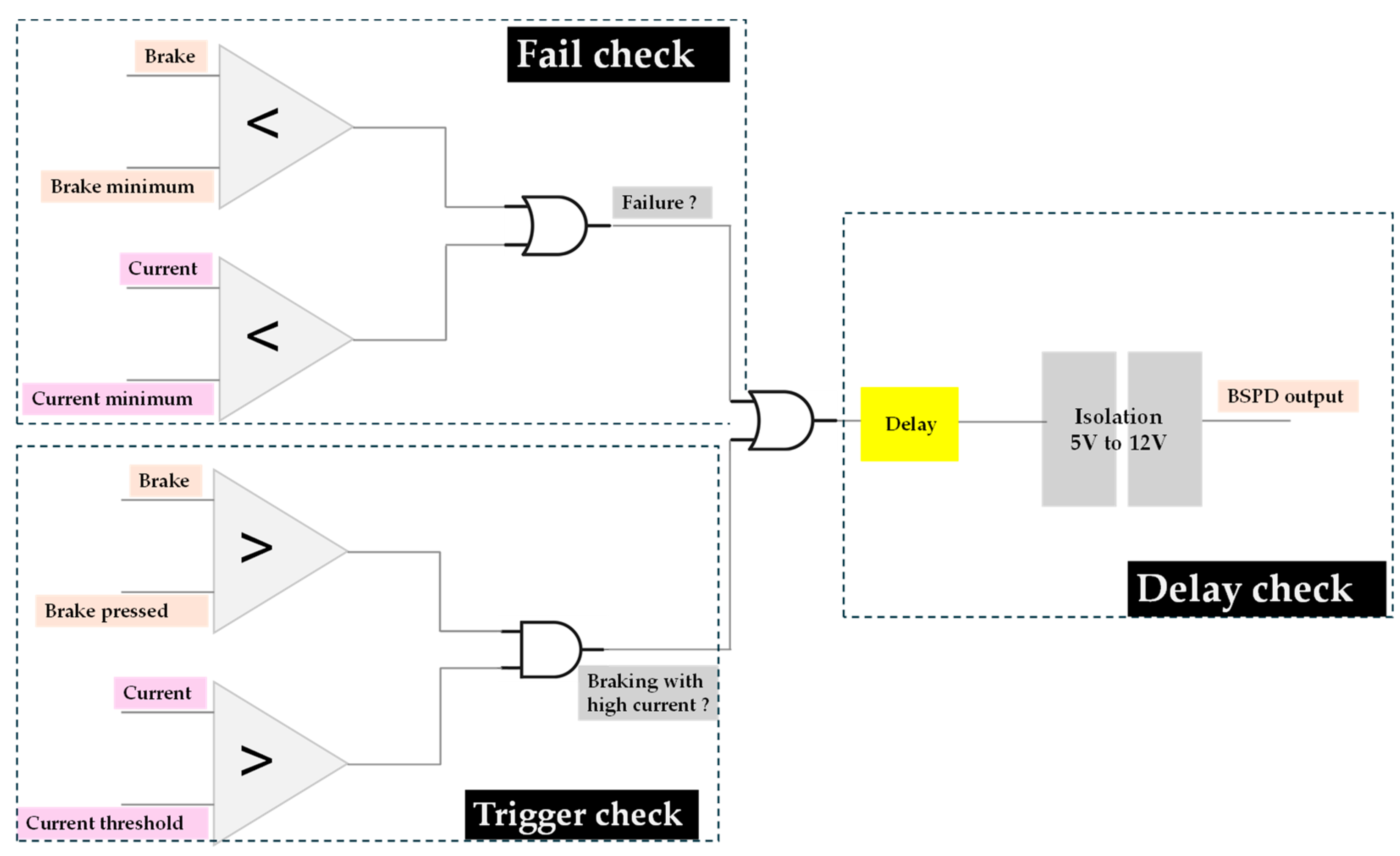
The BSPD EC is designed to detect the hard braking when the brake and accelerator pedals are applied simultaneously. The BSPD EC will trip the SD line when this situation occurs for the designed period, td < 500 ms, which will in turn disconnect the HV circuit by turning the AIRs off. As shown in Figure 8, the dc-link current IHV is continuously measured and compared to a threshold value Ith to check when a considerable current is flowing into the motor. The brake position sensor checks for the hard braking condition which is usually set to 30% of the brake travel. If the two conditions are present simultaneously and exceeded the allowed period td, the BSPD relay coil will be deenergised and the contact will trip the SD line to disconnect the HV circuit. It should be noted that the block diagram in Figure 8 is meant to explain the logic of the BSPD while the in-detail design will be presented in the next section.

2.3. IMD and AMS

Physically situated within the accumulator box, the insulating monitoring device (IMD) is connected electrically after the BSPD and before the accumulator management system (AMS). The primary role of the IMD is to continually assess the insulation between the LV and HV systems and trip the SD line if insulation falls below a specified threshold. The AMS, typically an output from the BMS, is responsible for tripping the SD line should any battery parameters exceed acceptable limits. The IMD and AMS signals are critical to ensure the safety of the FSERC. The IMD detects any wrong or loose connection between the HV and LV systems. As the LV ground is connected to the chassis of the car, the IMD measures the ohmic resistance between the chassis and the terminals of the HV systems. As long as this insulation resistance is higher than certain threshold (calculated as a function of the TS voltage), the IMD generates 12 VDC on its output pin. Once the insulation resistance falls below the threshold value, the output pin will generate 0 V instead.
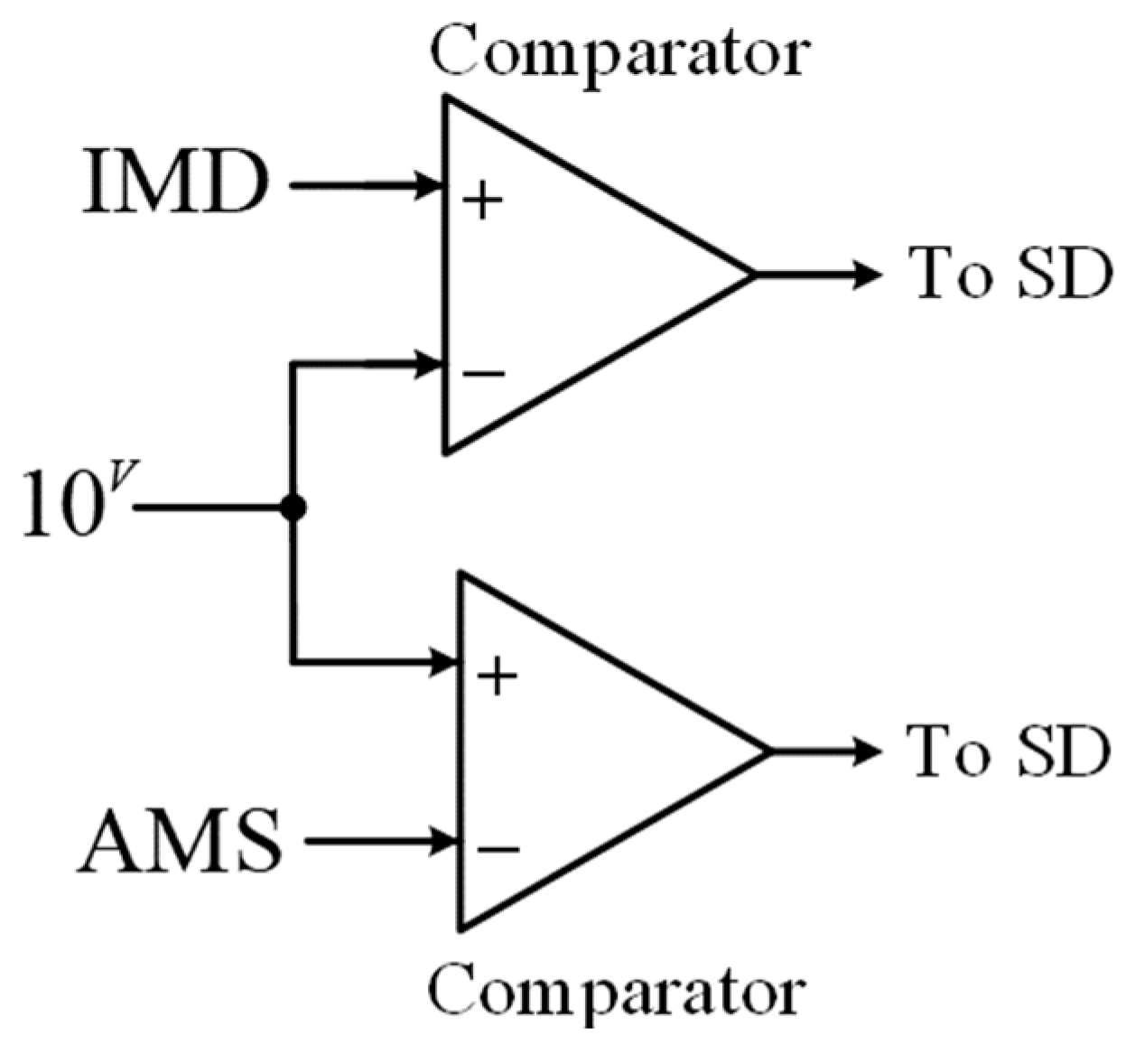
The AMS signal can be programmed by the ORION BMS software to detect for several errors such as battery cells min/max limits, cells temperatures, cells current…etc. Similar to the IMD, the BMS should be programmed to give 12 V at one of its outputs when the system is error-free. If any error is detected, this voltage should fall to 0 V. It should be noted that several BMSs allow the user to toggle the logic of the error signal to generate 12 V when the error is detected and 0V otherwise. This is not preferred in this application as the operation will not be fail-safe in case when the connection between the BMS and the detecting EC is broken for any reason. Figure 9 shows the basic logic of the IMD and BMS errors detection and interface with the SD line. The outputs of the comparators associated with the IMD and AMS circuits are incorporated in the safety shutdown (SSD) EC.

2.4. SSD Circuit

The SSD EC is responsible for incorporating the error signals from the BSPD, IMD, AMS, as well as the tractive system active light (TSAL) plausibility signal. The TSAL control will be presented in a following subsection. The SSD EC should guarantee that the SD line will not be activated without the intervention of the electrical safety officer (ESO) if a temporary error occurs and disappears. This is done by latching-off the output of the SSD EC as shown in Figure 10.
The ESOs are authorised to reset the SSD circuit if they are confident that the error signals have been cleared correctly. The SSD circuit is also responsible for sending the signals to the light indicators in the cockpit and other places in the chassis of the FSERC. When all error signals are cleared and the four stages are closed, the output voltage of the SSD EC will be 12VDC which will be directed to the SD buttons as shown in Figure 2.

2.5. Pre Charge/Discharge/Activation Logic Circuit

The pre-charge/discharger/activation logic (PDAL) EC is the most critical control circuit because it is responsible for turning the FSERC on and off by connecting the accumulator HV to the tractive system (TS) DC-link. To perform that safely, the PDAL is responsible for three main functions as follows:

2.5.1. Pre-Charge

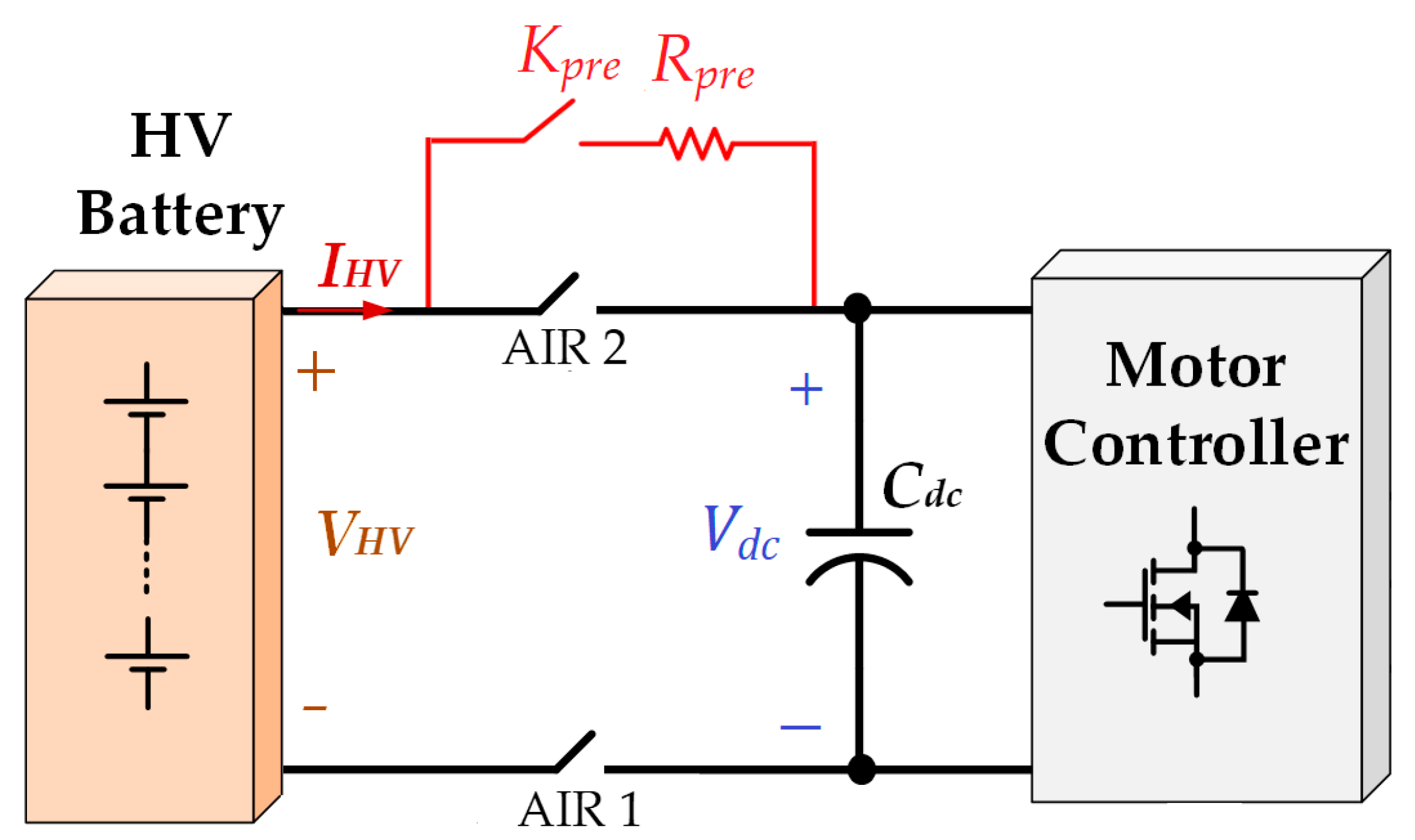
The PDAL ensures that the connection between the accumulator and the TS dc-link occurs in a smooth and safe operation. At the beginning of the operation, the dc-link voltage vdc starts from zero and the capacitor Cdc in Figure 11 should be empty of charge at the beginning of operation and therefore closing the two AIRs (AIR1 and AIR2) can cause a large inrush current as:
IHV = Cdc dvdc/dt
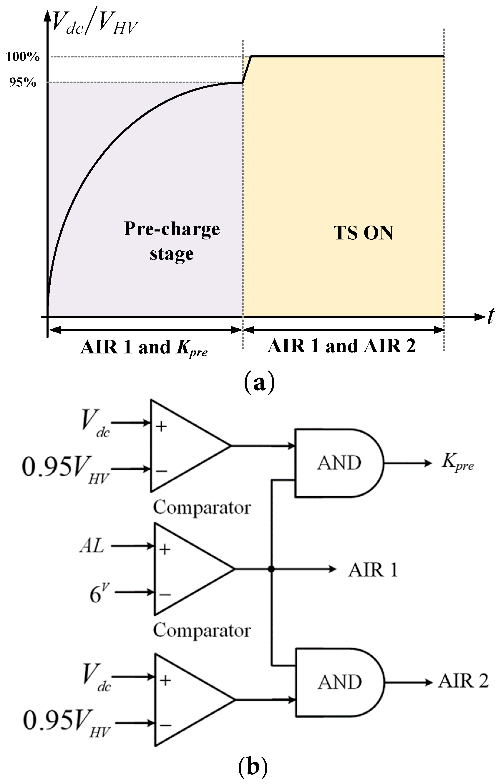
Accordingly, the dc-link capacitor needs to be charged via the top circuit with the NC relay (Kpre) and the pre-charge resistor (Rpre). Once the dc-link voltage reaches 95% of the accumulator voltage (VHV), the dc-link is allowed to be connected to the accumulator directly to start the operation normally.
Figure 12 shows the main logic of the Pre-charge part in the PDAL circuit. When the driver turns the system on and the AL voltage is high enough (e.g., above 6 V), the dc-link voltage is compared with the accumulator voltage to measure if it is below or above 95%. The time tdpre is meant to delay turning off Kpre until AIR1 is connected to ensure a proper overlap in between the two circuits. Once the pre-charge operation is done, the motor controller sees the full accumulator voltage and the FSERC is ready to start the operation.

2.5.2. Discharge

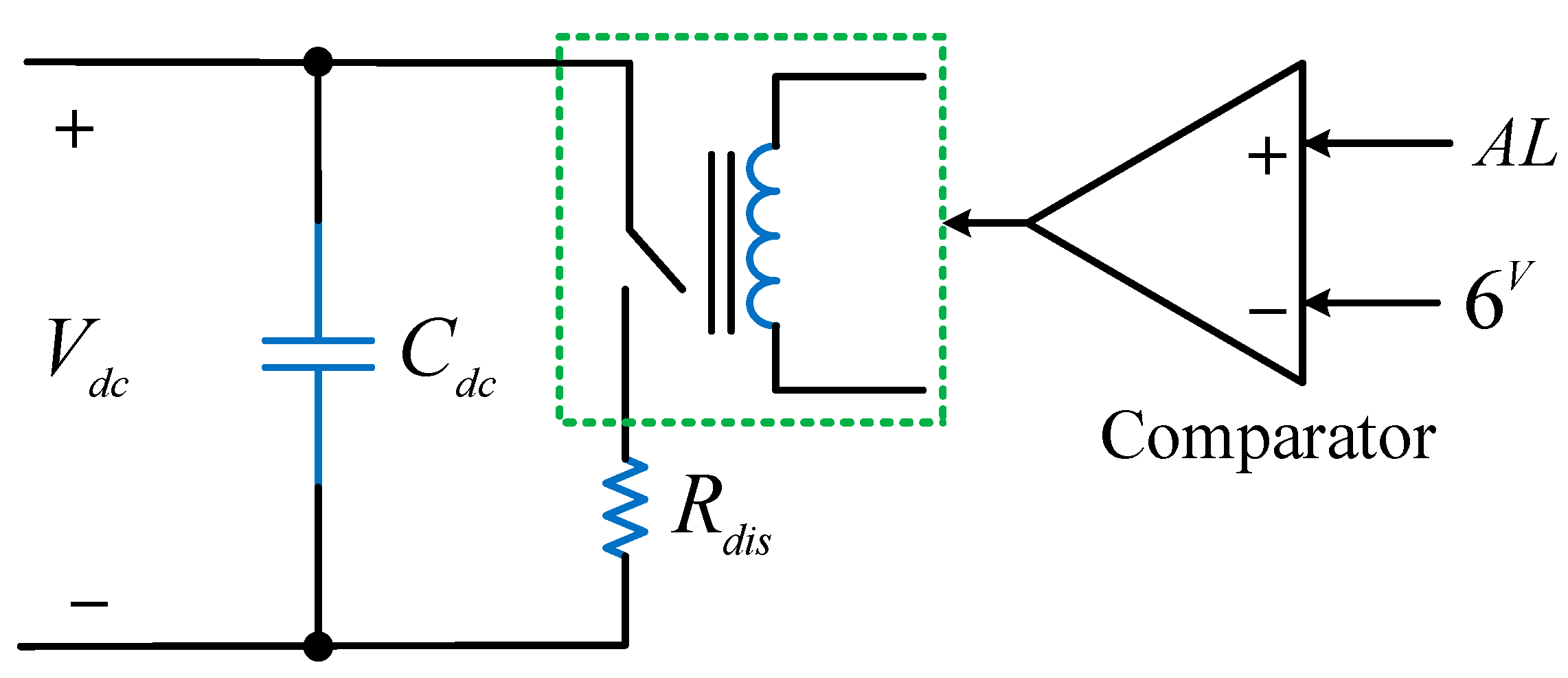
This is the second part of the PDAL EC with a responsibility to ensure that the dc-link capacitor is completely discharged and accordingly its voltage is zero when the TS is disconnected from the accumulator. The TS can be disconnected in purpose by the driver or due to any error resulting in tripping the SD line. Figure 13 shows the logic for the discharge EC when the discharge resistor Rdis is connected across the dc-link capacitor via the contact of a NC relay controlled by the input AL which comes from the activation logic EC.

2.5.3. Activation Logic

The AL function is very critical in the operation of the FSERC and should be designed carefully. This part is responsible for main four functions:
(1)
Turn on the TS when the driver is ready to start racing using a START button within the cockpit. This should start with the pre-charge stage as discussed in Section 2.5.1. For safety reason, the START button should be of a push-release type and therefore the PDAL should latch this command.
(2)
Turn off the TS when driver wants to disconnect the TS system using a STOP button within the cockpit. This should be followed by the discharge routine in Section 2.5.2 to ensure that the dc-link capacitor is completely discharged.
(3)
The PDAL should disconnect the TS when any error signal arises, an emergency button is pressed, or any switch is opened as shown in Figure 2. In this case, the PDAL should not allow for a re-start without clearing the error and resetting the SD line by the ESOs.
(4)
If the TS is needed to be disconnected as in (2) or (3), a delay should be given between the command and the action to allow the motor controller to turn off the PMSM rotating magnetic field (RFE) before disconnecting the TS circuit. This is to protect the semiconductor devices (such as IGBTs or MOSFETs) from the voltage and current spikes that may occur. Usually, a time delay of around 200 ms should be sufficient to ensure the safe operation of the motor controller.
A simple logic diagram for the AL functions in the PDAL circuit is shown in Figure 14. To ensure the safety of the operation, the PDAL controls the AIRs at the low side of the coils as shown in Figure 2. This adds to the design complexity of the PDAL EC especially with the necessity of the off delay tdPDAL as explained in point (4) above and when the resistance of the high current AIR coils are usually low (around 10 Ω) in the automotive market.

2.6. Tractive System Active Light

The main function of TSAL system is to indicate the TS status so the users know when the HV is present outside the accumulator. The TSAL EC controls a beacon fitted at the top of the chassis. The beacon, as shown in Figure 15, is created as a two-part assembly to show constant green and flashing red lights.
The red light is flashing continuously with a 50% duty cycle ratio and a frequency of 4 Hz. Both green and red lights are controlled by 12 V signals to meet the following requirement:
The TSAL light is green when only the LV is present at the vehicle side by turning the LVMS on. This indicates to the users that the FSERC is safe to approach and scrutinize.
The TSAL light is flashing red when any of the following is true:
(1)
AIR 1 or AIR 2 is on
(2)
Kpre is on
(3)
Vdc > 60 VDC
The actual (mechanical) status of the AIRs and the relays are considered in the design of the TSAL EC. This is because it might be possible that the intentional states of the coils are off while the contacts are closed due to any mechanical failure which means that HV maybe present while the users are not aware of the hazard. The discrepancy between the intentional and the mechanical state of any AIR or the pre-charge relay should be considered seriously and therefore the red light should be latched on until the ESOs check the issue. The truth table summarising the TSAL inputs and outputs is shown in Table 2.

2.7. Power Distribution Board

The power distribution board (PDB) aims to reduce the LVB energy consumption when the cooling system is on. As shown in Figure 16, the PDB will be activated when the temperatures of the accumulator and motor are above the threshold demanding the fans and the pump to be turned on. Meanwhile, the LVB will be limited to supplying energy to the rest of the LVCS ECs.
The PDB is designed to have a high efficiency and to provide a galvanic isolation between its inputs and outputs which is necessary to keep the HV and the LV systems isolated. If the galvanic isolation is not maintained, the IMD will sense a connection between the two systems resulting in tripping the SD line as mentioned in Section 2.5. To meet this requirement, the isolated DC/DC converter shown in Figure 17 is used to step down the HV to the 12 VDC required by the pump and fans.

2.8. Electronic Control Unit

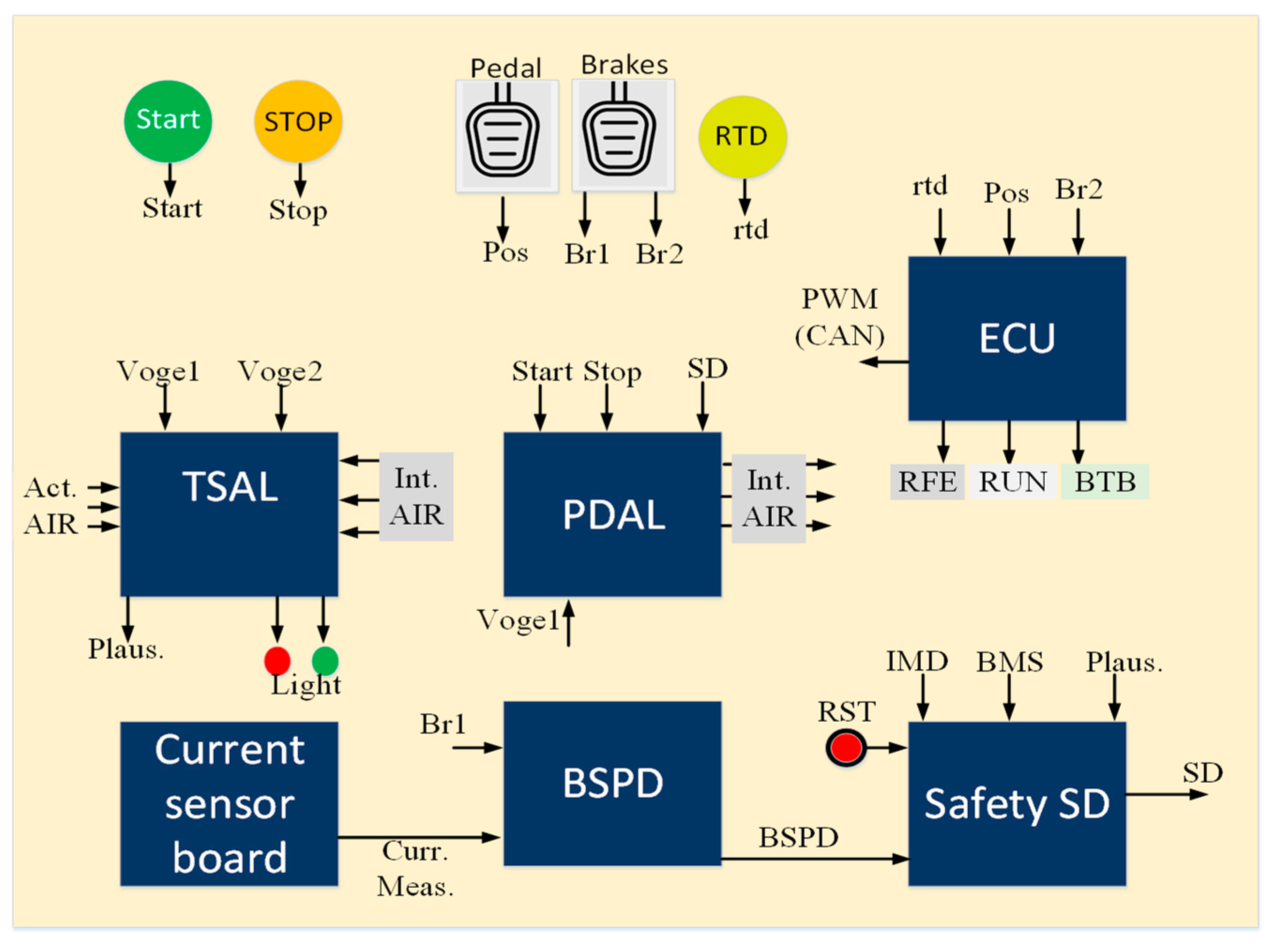
The electronic control unit (ECU) hosts the micro-controller (µC) and provides the required interface with several systems in the FSERC such as the acceleration pedal positioning system (APPS), brake system (BS), and the motor controller. This involves transforming the driver commands from the pedals to a torque demand request input into the motor controller, along with initialising and shutting down the motor controller, where necessary, via the enable signals as shown in the block diagram in Figure 18. The main input signals to the ECU are:
APPS and Brake sensors: these are analogue input voltages in the range 0–5 V.
Ready-to-drive (RTD) button: this is a push-release button connected to the 5 V rail. The driver presses the RTD button with the brake pedal to awake the FSERC program providing that the TS is active, and the pre-charge stage has passed.
PDAL input: the status of the AL is sent to the ECU to inform the motor controller when the TS is about to be disconnected and accordingly the RFE of the motor should be shut down as explained earlier in Section 2.5.3. As the PDAL EC operates at 12 V, this signal needs to be stepped down to 5 V to be compatible with the µC analogue-to-digital (A2D) inputs.
The main output signals of the ECU are:
Brake light control: the required voltage to turn on the red brake light at the back of the FSERC chassis. As the digital outputs (DOs) of the µC provide 5 V output voltages, opto-couplers are employed to provide the required 12 V voltage to the brake light circuit.
RTD Buzzer: to control the buzzer which gives an audible sound to the personnel indicating that the FSERC is ready to race.
Enable signals: 12 V signals to start and stop the motor controller.
Motor controller torque/speed command: this is an analogue 12 V signal to control the torque/speed of the motor.

3. Build Instructions

It is important to design the EC printed circuit boards (PCBs) in the simplest possible way to ease the testing, soldering, and troubleshooting them when there is any fault. The PCB schematics are designed using KiCad®(2024) as it is an open source and free software which facilitate the design and simulation process. Each circuit was designed and tested separately. However, some amendments were necessary when issues occurred during the interface process.

3.1. BSPD

The detailed schematic for the BSPD EC is provided in the Supplementary Files of the paper. Connector J1 receives the measurement from the current sensor as an analogue signal between 0–5 V which represents the accumulator output current between 0–200 A. J2 is connected to the brake sensor to detect the hard braking. Connectors J4 and J6 are sending output signals to the SSD and PDAL ECs to inform about the status of the BSPD.
Figure 19 shows a simplified diagram for the overall schematic which consists of the three main stages that will be explained in the following subsections.

3.1.1. Fail Check

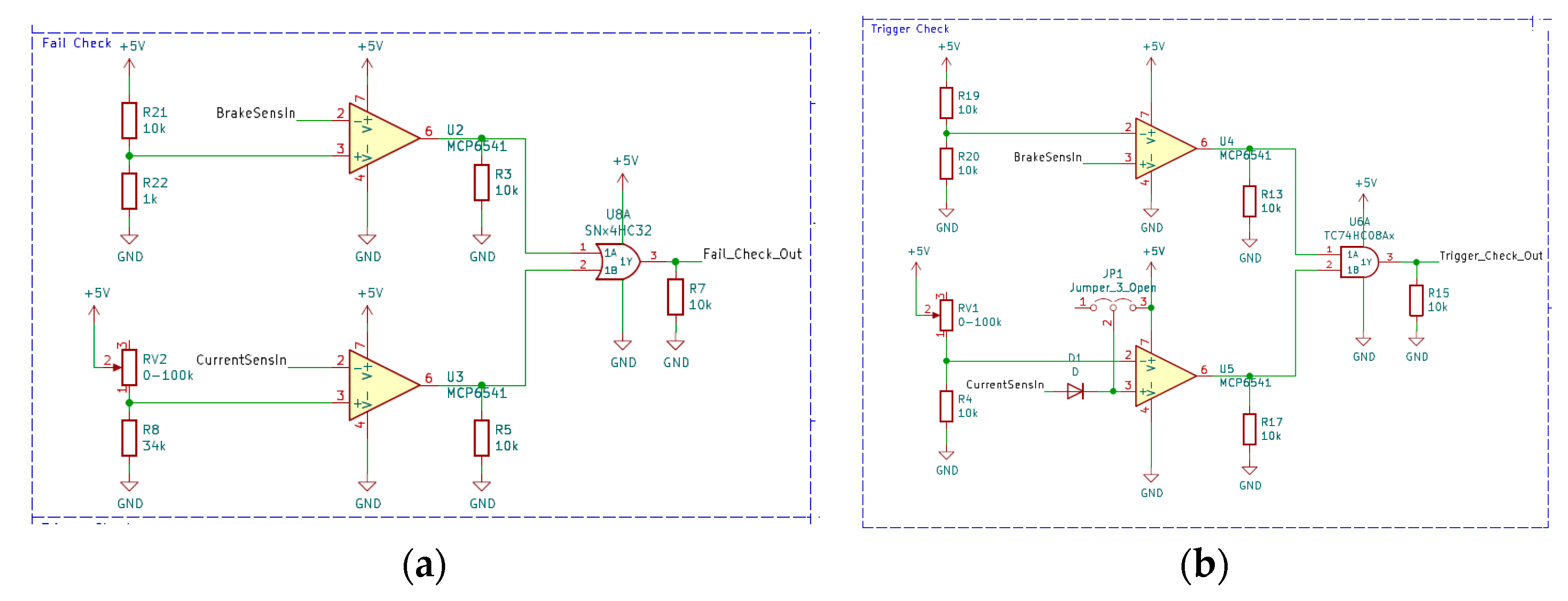
This part is responsible for checking that the received signals from the current and brake sensors are intact and kept with the expected range. To ensure a fail-safe operation, it is important to ensure that the readings are not low due to any cut in the wires between the brake pedals and the BSPD circuit. As shown in Figure 20a, high-speed differential comparators are employed to ensure that that the measurements do not fall below a specific threshold which can be pre-set using potentiometers in the voltage divider circuits. If any of the conditions is violated, the output of the stage will be high (≈5 V).

3.1.2. Tigger Check

The input signals, if healthy, will be compared with the threshold voltages to check if the two conditions are high together using an AND gate as shown in Figure 20b.

3.1.3. Power and Delay Stage

The NO contact of relay K1 is connected in series with the SD line and will be closed only if pin 1 in K1 is pulled down to the ground (GND). To pull pin 1 to GND, device Q1, which is an n-type metal–oxide–semiconductor field-effect transistor (MOSFET), is used. This condition will be satisfied only if the inputs from the fail-check and trigger-check stages are both low because they are connected as inputs to the OR gate U7A. The RC circuit composed of R9, R6, and C4 is designed to delay the tripping in case if the driver released the brake pedal with the 500 ms period.

3.2. SSD

Figure 21 shows the overall schematic of the SSD EC while the detailed is provided in the Supplementary Files of the paper. To simplify the design process, the four stages use the same modular power stage which is controlled by a 12 V control signal.
The control section is detailed in Figure 22a with the three identical series stages. The modular design of each stage, shown in Figure 22b, consists of p-type MOSFET and npn bipolar junction transistor (BJT) with their drive resistors. If the control input is high (≈12 V), the BJT will be on keeping the gate voltage of the MOSFET will be below the threshold. Thus, the MOSFET will conduct the SD current to the next stage and the output voltage will be 12 V. When the control input falls, the BJT will be turned off and the MOSFET gate voltage will be increased to 12 V. Consequently, the MOSFET will be turned off and the SD line will be disconnected at this stage. After the IMD, AMS, and the BSPD stages, the latching relay will keep the SD line disconnected in case of any error until the ESOs reset the line again provided that the three stages are fault-free. The TSAL stage come after the latching relay and therefore is allowed to clear itself.

3.3. PDAL

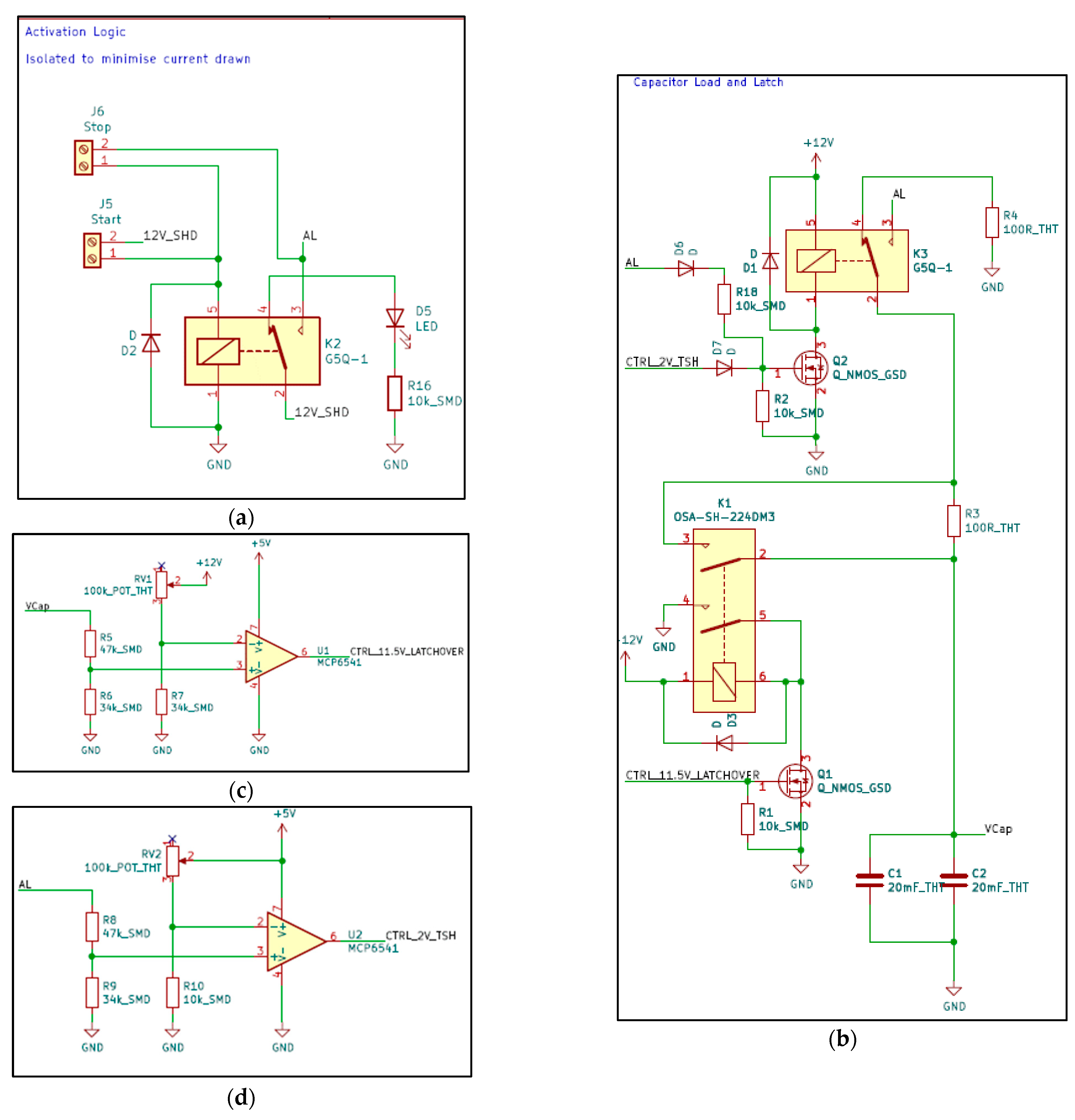
The detailed schematic of the PDAL EC is provided in the Supplementary Files of this paper. The top left part of the circuit receives the signals from the start and stop push-release buttons that are installed in physically in the cockpit. The breakdown of the PDAL stages is shown in Figure 23. Figure 23a shows the AL part. If the start button at J5 is pressed when the SD line is healthy, the relay K2 will latch the 12 V input from the SD line at pin 2 to the AL output at pin 3. The AL will be latched at 12 V until the driver presses the stop button connected to connector J6 or the 12 V supply at pin 2 is cut due to an error or disconnection in the SD line. Figure 23b shows the process for charging two parallel capacitors C1 and C2 that through the resistor R3. It should be noted that this is different to the pre-charging stage for the dc-link capacitor which is connected to the MC. C1 and C2 are responsible for creating a time delay in the SD path which is responsible for protecting the MC. This delay is required to inform the MC that the SD line is going to disconnect so the rotating magnetic field is turned off using the RFE signal from the PDAL circuit to the MC. The comparison in Figure 23c will latch C1 and C2 to the SD line once a threshold voltage has been exceeded. The comparison in Figure 23d will disconnect the AIRs when the voltage falls below a certain threshold. The battery voltage is compared to the dc-link capacitor voltage as shown in the pre-charge stage in Figure 23e. When the dc-link voltage exceeds 95%, the control signal of the positive relay (AIR2) turns is high while the control signal of the pre-charge relay is low. The low-pass filter C4 and R14 creates a short delay to ensure a proper overlap between the relays to avoid arcing during transition. The coils of the AIRs and pre-charge relays are connected to connector J1 while the information about the states is sent through the other connectors.

3.4. TSAL

The detailed schematic of the TSAL EC is provided in the Supplementary Files of this paper. The top left part of the circuit receives the actual states of the AIRs at connectors J4 and J6 which are connected to the auxiliary contacts of the AIRs. The intentional states of the AIRs, generated by the PDAL circuit, are connected to connector J8. The TSAL also needs information about the dc-link and accumulator voltages as well as the status of the SD line. The TSAL outputs the control signals for the red and green LEDs at J2 and J3 respectively. The main stages of the TSAL circuit are explained in the following subsections.

3.4.1. Green Light Control

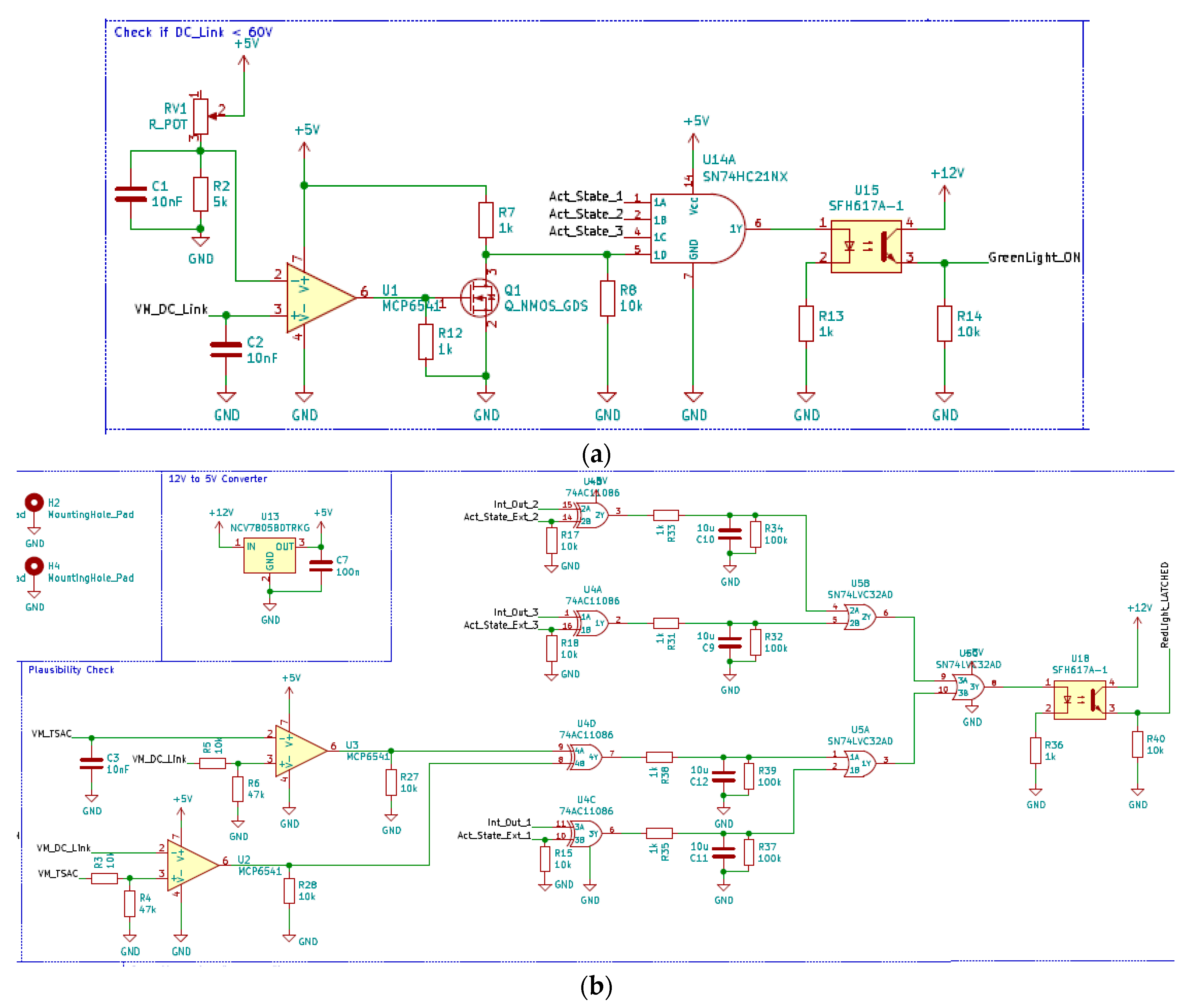
The control signal will be activated only if the three AIRs are off, and the dc-link voltage is below the threshold (60 V in this case). This is to guarantee that there is no HV present outside of the accumulator box and turn on the green light accordingly. As shown in Figure 24a, the optocoupler U15 will be activated with output voltage ≈ 12 V when the output of the AND gate U14A at pin 6 is high. This is achieved when the outputs of the AIRs actual states, indicating AIRs are off, and the voltage comparison at U1, indicating no HV presence, are all high. If any of these four conditions are violated, the green light control signal will be low (≈0 V).

3.4.2. Red Light Control

The plausibility check in Figure 24b is designed to achieve the truth table in Table 2.
If this part senses any implausibility between the actual and the intended states of the AIRs, the red light will be turned on and latched until the ESOs checks the issue.

3.4.3. Green and Red Lights Power Stage

Finally, this part will convert the control signals to the power signals with the suitable currents to power the LEDs. Relay K2 will latch the red light on and report the error to the SSD circuit in case of any implausibility while K1 switches the lights between green and red during normal operation.

3.5. PDB

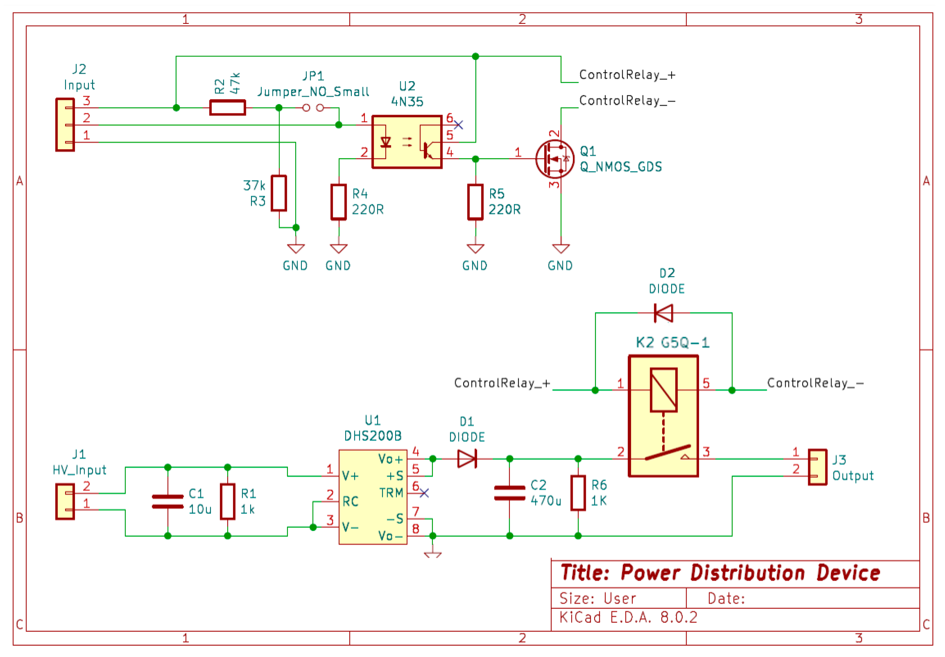
As shown in the schematic in Figure 25, the control signal for the PDB is connected to pin 2 at connector J2. This can be either a manual signal in the cockpit where the driver can turn the system on and off or it can be an automatic signal connected to the MC. The automatic signal can be programmed by the MC STM32 software where the voltage becomes high when a certain temperature is exceeded. When the motor’s temperature exceeds the threshold, which was set to 45°, the U2 optocoupler will be activated and turn the n-type MOSFET Q1 on. Accordingly, the relay K1 will be turned on and hence the power will be flow from the TS to the LV system.

3.6. ECU

The ECU, which its schematic is provided in the Supplementary Files, is designed to interface the signals from the APPS, BS, RTD button, and the Buzzer to the Nucleo-F303RE µC. The ECU will also interface the output signals of the µC at 5 V to the rest of the LVCS at usually 12 V. The signals of APPS1, APPS2, and BS potentiometers are connected to the analogue inputs A0, A1, and A2 of the µC. MOSFETS Q1 and Q2 are used to power the brake light at the back of the FSERC and the Buzzer at 12 V. Optocouplers U4-U5 are used to convert the 5V digital outputs from the µC to the 12V RFE, BTB, RUN, and pulse-width modulation (PWM) signals required to operate the MC [13]. The ECU also interfaces the controller area network (CAN)-bus which is a good option to control and get useful data from the MC about the speed, torque, voltage…etc. The ECU has several LEDs and test points that are needed for monitoring and troubleshooting.

4. Operating Instructions

The designs in the schematics presented in Section 3 are converted to Gerber format files using the KiCad® software so the PCBs can be manufactured and operated.

4.1. BSPD

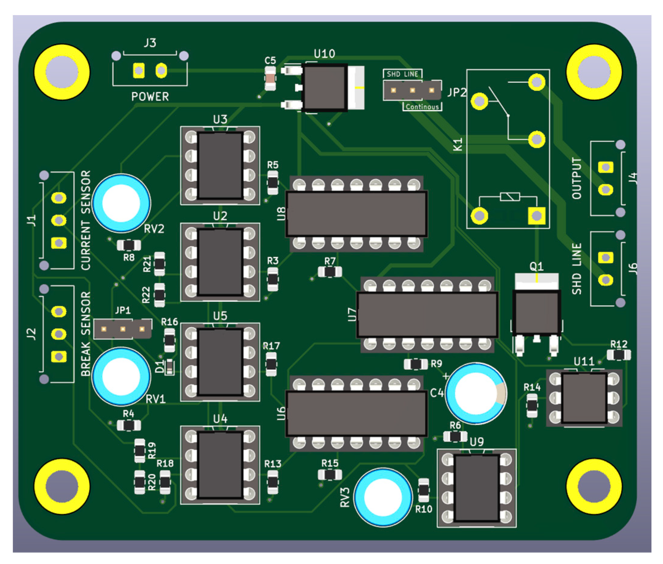
The BSPD PCB are shown in Figure 26. The circuit is powered by the 12 V rail and then it supplies the integrated circuits (ICs) through a 12 V-to-5 V regulator. It should be noted that the traces connected to the K1 relay’s contact should be designed according to the value of the SD line current required to energise the coils of the AIRs and the pre-charge relay. The main electronic components required to build the circuit are listed in Table 3.

4.2. SSD

The SSD PCB are shown in Figure 27. The circuit is powered by 12 V from the LV input. The push-release reset button is connected in series with the shoulder input. The three control signals for the IMD, AMS, and BSPD are fed from the signal connector at the left. The LEDs on the PCBs are added to inform about which stage is faulty. The electronic components required to build the circuit are listed in Table 4.

4.3. PDAL

The PDAL PCB are shown in Figure 28. The bottom part has the comparators and logic gates while the top part has the parallel capacitors and latching relays. The connection between the two parts is made possible using wires soldered at the back of the top part and the front of the bottom part. The main electronic components required to build the circuit are listed in Table 5.

4.4. TSAL

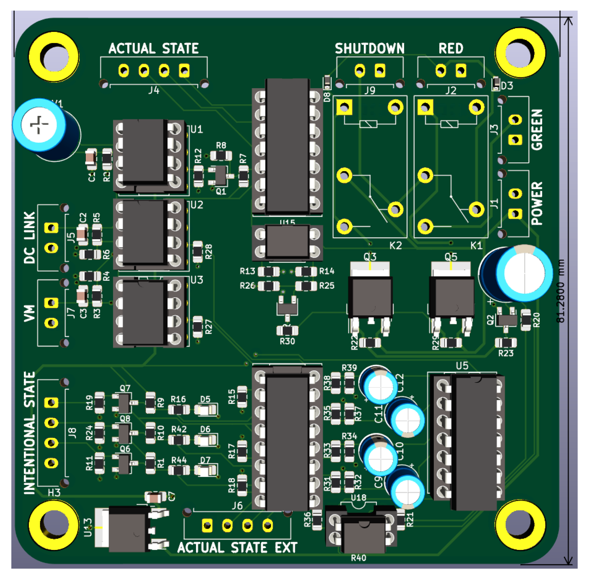
The front and back of the TSAL PCB are shown in Figure 29. The main electronic components required to build the circuit are listed in Table 6.

4.5. PDB

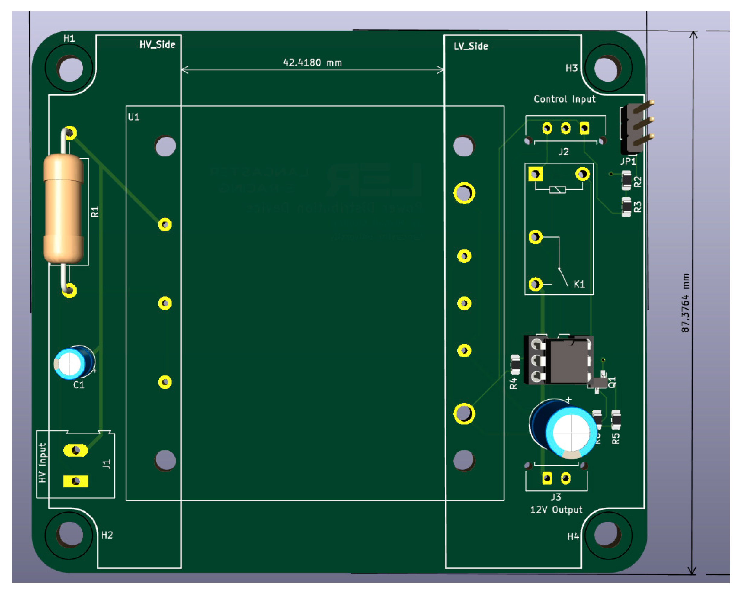
The front and back of the TSAL PCB are shown in Figure 30. The main electronic components required to build the circuit are listed in Table 7.

4.6. ECU

Figure 31 shows the final design for the ECU circuit where the board was designed to allow either an Arduino Uno R3 or the Nucleo Board to be mounted with space in the top side to allow a connector to be plugged in while mounted on the PCB. The two µCs have been chosen because they both shave the same analogue and digital inputs and outputs. The components were placed in a way to minimise the size of the board as the Arduino and Nucleo boards are already quite big, restricting the minimum size of the board. The main electronic components required to build the circuit are listed in Table 8.

5. Validation

To validate the LVCS, the different PCBs are connected to each other with the system as shown in Figure 32. Several tests are conducted to show the operation of the ECs when they are integrated together.

5.1. BSPD

The operation of the BSPD is shown in Figure 33 when it was connected to the brake current sensor. In the top graph, the dc-link current was controlled to be around 15 A when the AIRs are closed. The second graph shows the brake signals when they are pressed two times at t1 = 2.2 s and t2 = 5.1 s. As shown in the third graph, the driver released the brake before the RC delay circuit voltage reaches the threshold which is set by the voltage divider to be around 2.8 V. In the second time, the driver kept the brake pressed for longer than the allowed period which is set to 300 ms and hence the coils of relay K1 are de-energised leading the SD line voltage in the bottom graph to be zero which will need to be restarted and the ESO to recycle the power.

5.2. SSD

Figure 34 shows the operation of the SSD when it starts without errors and therefore all control signals are high (≈12 V). The IMD error is simulated at t1 = 2.1 s by disconnecting the control signal and therefore the output voltage of the SSD EC falls to 0 V. The IMD error was cleared at t2 = 4.2 s but the output voltage of the SSD will not go to 12 V until the ESO reset the SSD manually at t3 = 4.95 s. The SSD will then be active until another error happens.

5.3. PDAL

Two tests have been conducted to check the performance of the PDAL and ensure proper turning on and off for the TS. During this test, the FSERC was lifted up and the LV box was opened to check the LEDs in the SSD and PDAL ECs.

5.3.1. Turning the TS on

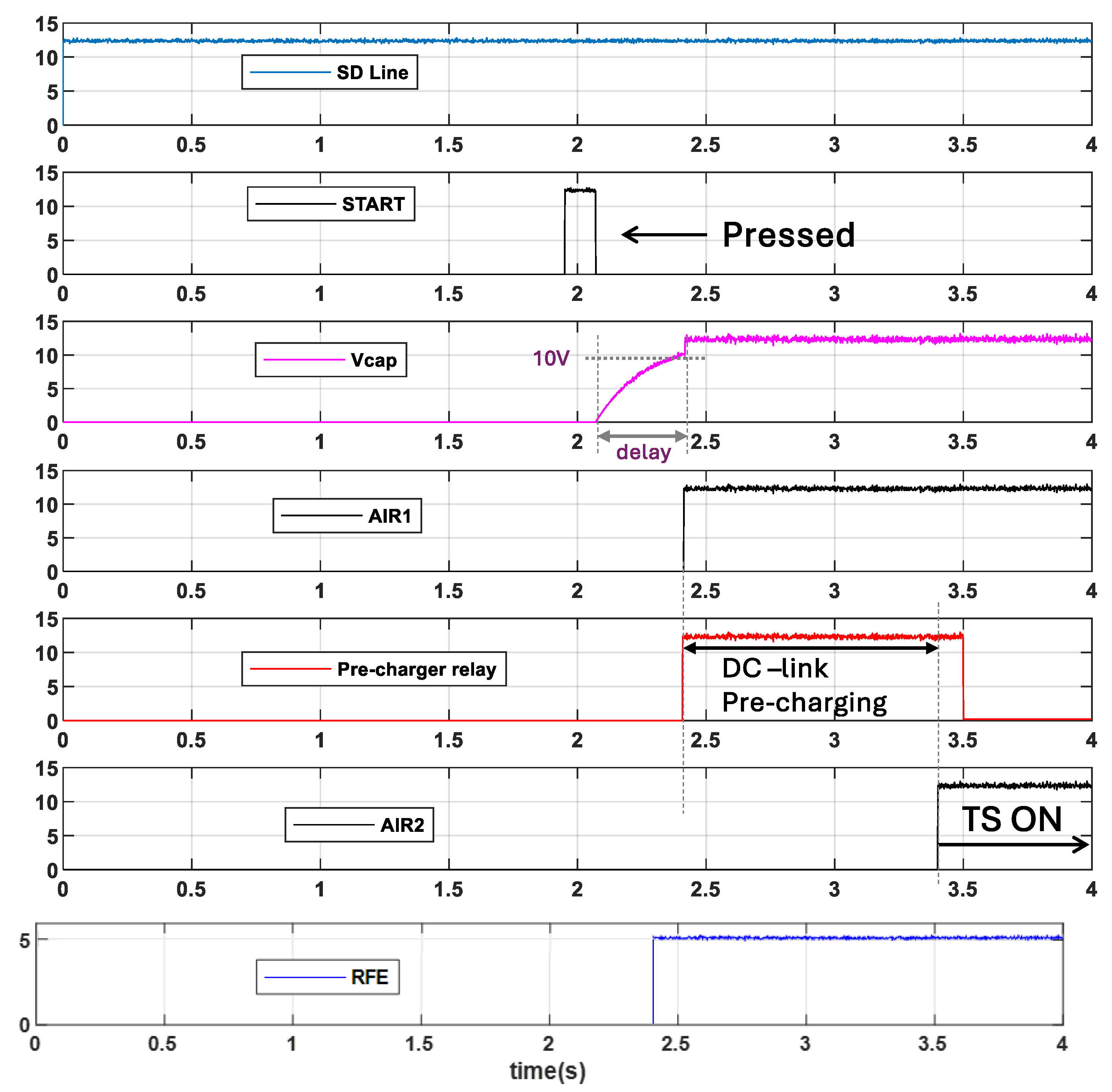
The dc-link starts from 0V as all AIRs are open and the dc-link capacitor is discharged by the discharge relay. As shown in Figure 35, the SD line is turned on by the SSD circuit at to = 0 s. The driver then presses the start button at t1 = 1.96 s and therefore the parallel capacitors’ (C1 and C2) voltage starts to increase gradually through R3 in the PDAL EC. When their voltage (Vcap) exceeds the threshold (10 V in this test) at t2 = 2.41 s, AIR1 is turned on connecting the negative pole of the accumulator to the dc-link. The pre-charge relay is turned on at the same time, so the dc-link capacitor is charged. At this moment, the RFE signal is sent to the MC to inform it that the TS is about to turn on. Once the pre-charge stage is finished at t3 = 3.42 s, AIR2 turns on to connect the positive pole of the accumulator to the dc-link. Thus, the TS is on and the FSERC is ready to enter the ready-to-drive mode. It should be noted that from t2, the SD line is connected directly to the capacitors C1 & C2 as R3 is shorted by K1.

5.3.2. Turning the TS off

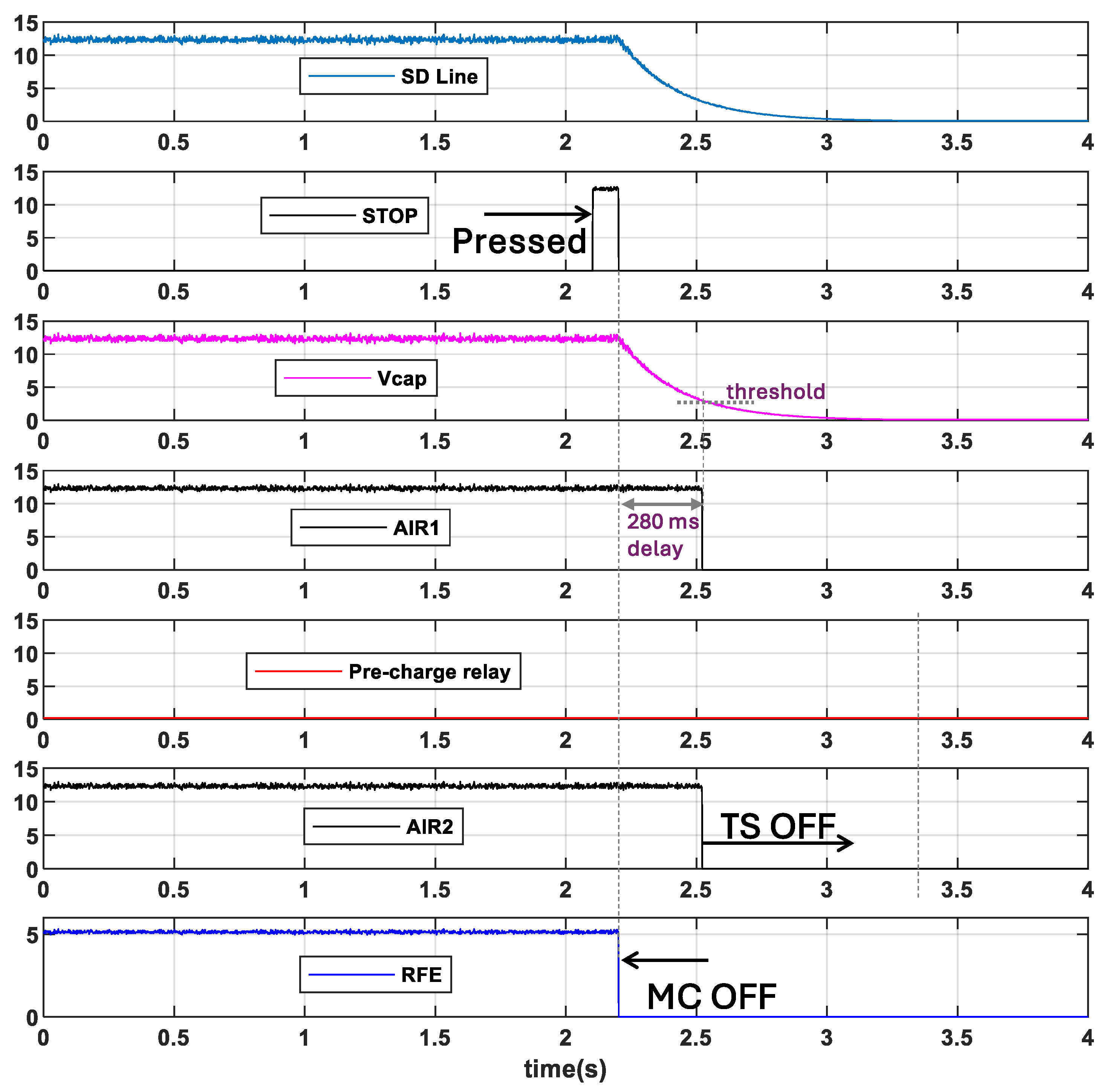
In Figure 36, the driver pressed the stop button at t1 = 2.2 s to command the TS to be turned off. Shortly after t1, the RFE signal becomes low to inform the MC that the TS is turning off soon. The parallel capacitors C1 & C2 starts to discharge in the coils of AIR1 and AIR2 which are measured to be ≈12 Ω each. The voltage of the capacitors continues to decrease until it reaches the pre-set threshold (2.7 V in this test) at t2 = 2.52 s. The threshold can be adjusted by the voltage divider circuit connected to the comparator U2 in Figure 23d. This is important to set the time delay between t2 and t1 which is required to protect the MC. The values of the resistors in the voltage divider circuit were chosen to keep the delay around 280 ms in this test. From t2, the TS is off, and the discharge resistor will be connected in parallel with the dc-link capacitor to discharge it in less than 5 s. The TS is then ready for a new cycle.

5.3.3. TS off Due to an SD Line Error

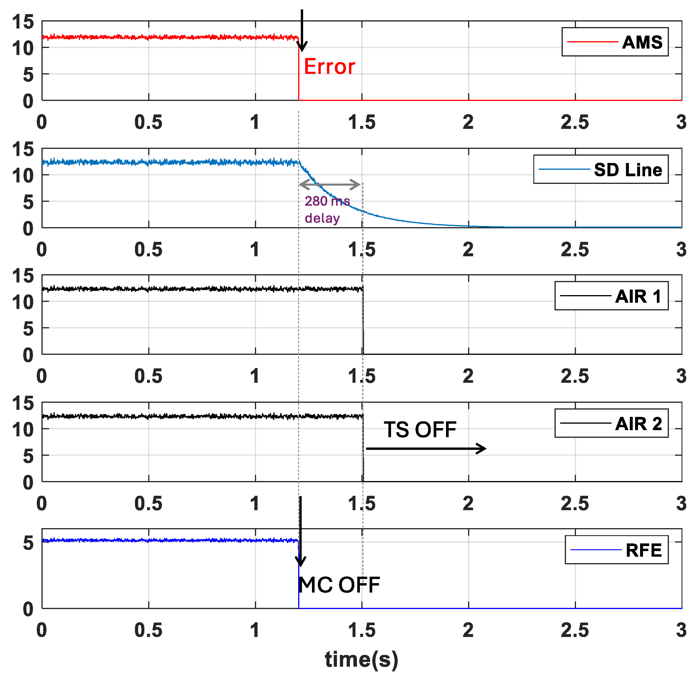
The action of disconnecting the TS due to an error in the SD line is tested when the AMS error is performed deliberately by disconnecting one of the temperature measurement sensors. As shown in the top graph in Figure 37, the AMS senses the error and therefore its output voltage falls to 0 V at t = 1.2 s causing the SD capacitors to start the discharge process as shown in the second plot. At the same instance, the PDAL EC informs the MC to turn off the enable signal to the PMSM rotating magnetic field as required. After a delay of 280 ms, the two contactors AIR 1 and AIR 2 are turned off so the TS is turned off. The AMS indicator LED in the SSD EC, shown in Figure 27, is turned off to help the team members with troubleshooting the problem caused by losing the temperature sensor.

5.4. TSAL

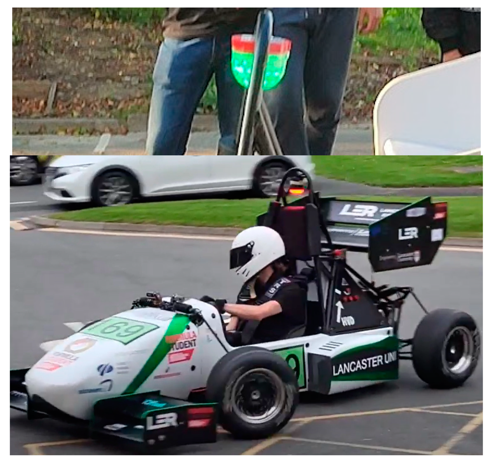
The performance of the TSAL was tested firstly on the bench with manual switches mimicking the inputs and outputs. Then, the operation has been tested by visual inspection during real operation as shown in Figure 38 to ensure that it fulfils the requirements in Table 1. The TSAL plays an important role in informing the drivers and ESOs about the status of the TS and therefore it a redundant small 12 V battery was added in parallel to the main LVB. It should be noted that the beacon is able to change the frequency of the red flasher internally. However, if a flasher beacon is not available in the market, the output of the TSAL circuit should be modified with a PWM controller to adjust the frequency of the red light. This controller can be added after relay K1 in the TSAL circuit.

5.5. LVB

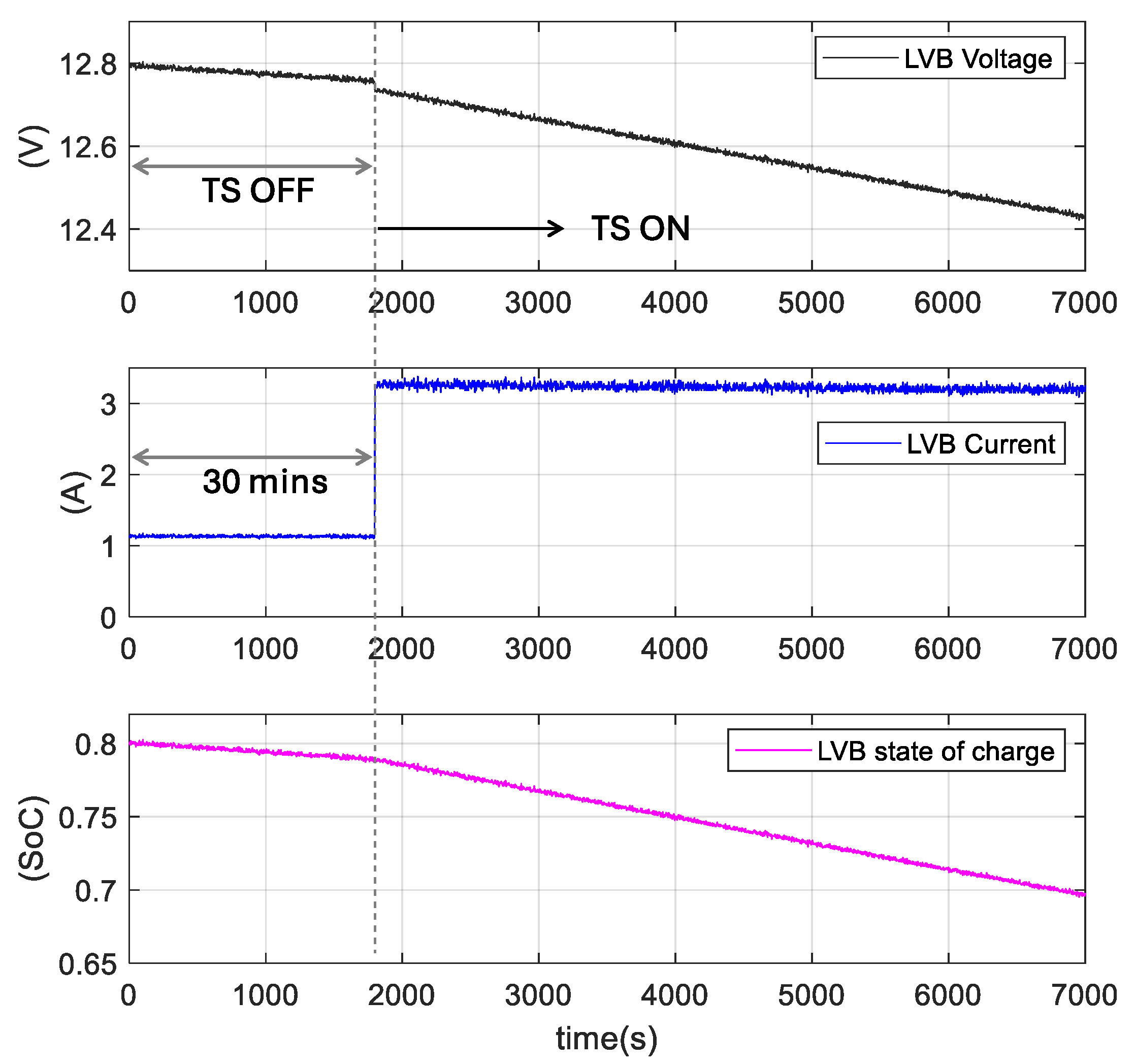
With the LVCS turned on, Figure 39 shows the voltage, current, and the state of charge (SoC) of the 50 Ah LVB supplying the whole system. The results were recorded when the LVMS is turned on when the SoC of the LVB is 80% and the terminal voltage is 12.8 V. For the first 30 min, the TS is turned off and hence the drawn current supplies the LVCS excluding the AIRs. Then, the TS is turned on via the AIRs and therefore the LVB current increases from 1.13 A to 3.275 A. The LVB is keep operating at this discharge rate for 2 h, so its SoC is reduced to 70% with a drop in the terminal voltage to 12.4 V. The LVB will reach SoC = 20% after 8 h of operation and hence the terminal voltage will decrease to 11.4 V. The tolerance voltages of the LVCS components, including voltage regulators, comparators, switches, and relays’ coils, are selected so they can function at voltages below the minimum expected LVB of 11.4 V.

5.6. PDB

The PDB EC plays an important role in saving the LVB energy to ensure the operation presented in Section 5.5 and Figure 39. The operation of the PDB is shown in Figure 40 where the PMSM starts from standstill at a temperature of around 27.5 °C. As shown in the bottom graph, the temperature increases until it reaches 45 °C at around 9.6 min of operation at the top speed. When this threshold temperature is reached, the opto-coupler U2 in the PDB EC, shown in Figure 25, is turned on activating the pump and fans system. Thus, rate of temperature rise is reduced until it settles at a value in the range of 50 °C to 60 °C. It is worth noting that the maximum value in the MC program is set to 60 °C before beyond which the MC will stop the process.

6. Conclusions

The paper presented the design of the LVCS which controls the racing car built by the 2022 LER team. The system is designed to fulfil the IMechE rules, that are put in place to ensure the safety of the operation, and to improve the performance of the FSERC. The LVCS operates mainly at 12 V and supplied from a relatively small LVB which is crucial in satisfying the functionality and the durability conditions. One of the main goals achieved by the LVCS in this work is to minimise the current, and hence the power, absorbed by the LVB so the operational time can be extended. The ECs are designed to be as simple as possible in order to ease their troubleshooting and maintenance processes without compromising the safety regulations. All ECs are equipped with accessible monitoring LEDs to help in identifying the source of faults when they occur. The paper presented a discussion on the effect of the ECs on the performance of the car during acceleration, top-speed operation and during braking using the PMSM model, mathematical analysis, and computer simulations, showing the relation between the hard braking torque and the HV battery power. The ECs are designed so the major functions affecting the safety of the FSERC are fail-safe meaning that the TS will be disconnected and de-energised when any of the components fails, is removed, or damaged. It was taken into consideration that the FS projects usually have limited budgets and hence most of the employed devices in the system are chosen as standard components that are available in the market at reasonable cost. The LVCS have been tested on bench and during operation where experimental results have been provided to show the performance of the circuits.

Supplementary Materials

The following supporting information can be downloaded at: https://www.mdpi.com/article/10.3390/hardware2030010/s1.

Author Contributions

Conceptualization, S.S., J.T.H., J.L.I., J.H., K.M., J.E. and W.H.; methodology, A.D.B., S.S., J.T.H., J.L.I., J.H., K.M. and J.E.; software, A.D.B., S.S., J.T.H., J.L.I., J.H., K.M. and J.E.; validation, A.D.B., S.S., J.T.H., J.L.I., J.H., K.M. and J.E.; formal analysis, S.S., J.T.H., J.L.I., J.H., K.M., J.E., W.H., A.D.B. and F.N.E.; investigation, A.D.B., S.S., J.T.H., J.L.I., J.H., K.M., J.E. and F.N.E.; resources, A.D.B. and A.D.; data curation, A.D.B., A.D. and F.N.E.; writing—original draft preparation, A.D.B. and F.N.E.; writing—review and editing, F.N.E., A.D.B. and A.D; visualization, S.S., J.T.H., J.L.I., J.H., K.M., J.E. and W.H.; supervision, A.D.B. and A.D.; project administration, A.D.B., A.D. and F.N.E.; funding acquisition, A.D.B. and A.D. All authors have read and agreed to the published version of the manuscript.

Funding

This work was supported by the School of Engineering at Lancaster University.

Institutional Review Board Statement

Not applicable.

Informed Consent Statement

Not applicable.

Data Availability Statement

The original contributions presented in the study are included in the article/Supplementary Material, further inquiries can be directed to the corresponding author.

Acknowledgments

The authors would like to thank the mechanical group of the LER 2022 team: Thomas Pagen, Darina Antonova, James T. Whitfield, Joshua Dean, Dragos Culica, Joseph Lowe, Jake Donnelly, Aaron Loi, Will Harwood, Alex Jones, Erin Kerley, Derek Seward, and Nicolas Renninson for their extraordinary contribution to the mechanical side of the FSERC. Also, the authors would like to thank Milliamp Technologies Ltd. ([email protected]) for their continuous support to the LER team.

Conflicts of Interest

The authors declare no conflict of interest.

Nomenclature

AMSAccumulator Management SystemLVBLow Voltage Battery
APPSAccelerator Pedal Position SensorLVCSLow Voltage Control System
BMSBattery Management SystemLVMSLow Voltage Master Switch
BOTSBrake Over-Travel SwitchPCBPrinted Circuit Board
BSPDBrake System Plausibility DevicePDALPre-charge Discharge Activation Logic
BPPSBrake Pedal Position SensorPDBPower Distribution Board
ECElectronic CircuitPMSMPermanent Magnet Synchronous Motor
ECUElectronic Control UnitSDShutdown
FSERCFormula Student Electric Racing CarTSTractive System
HVHigh VoltageTSMSTractive System Master Switch
HVDHigh Voltage DisconnectTSALTractive System Active Light
IMDInsulation Monitoring Device

References

  1. Lai, N.Y.G.; Foo, W.C.; Tan, C.S.; Kang, M.S.; Kang, H.S.; Wong, K.H.; Yu, L.J.; Sun, X.; Tan, N.M.L. Understanding Learning Intention Complexities in Lean Manufacturing Training for Innovation on the Production Floor. J. Open Innov. Technol. Mark. Complex. 2022, 8, 110. [Google Scholar] [CrossRef]
  2. Tarle, N.; Kulkarni, R.; Desale, N.; Pawar, V. Design of a Battery Management System for Formula Student Electric Race Vehicle. In Proceedings of the 5th International Conference on Computing, Communication, Control and Automation (ICCUBEA), Pune, India, 19–21 September 2019; pp. 1–6. [Google Scholar] [CrossRef]
  3. Carraro, E.; Degano, M.; Morandin, M.; Bianchi, N. Formula SAE electric competition: Electrical motor design. In Proceedings of the Electric Machines & Drives Conference, Chicago, IL, USA, 12–15 May 2013. [Google Scholar]
  4. Akop, M.Z.; Rosli, M.A.M.; Mansor, M.R.; Alkahari, M.R. Soft skills development of Engineering undergraduate students through Formula Varsity. In Proceedings of the International Conference on Engineering Education (ICEED), Kuala Lumpur, Malaysia, 7–8 December 2009; pp. 106–110. [Google Scholar] [CrossRef]
  5. ImechE Formula Student Rules. Available online: https://www.imeche.org/events/formula-student/team-information/rules (accessed on 31 July 2024).
  6. Biswas, A.; Yadav, R. Modeling and Simulation of Launch Control System for Formula Student Electric Vehicle. In Proceedings of the 2021 IEEE Transportation Electrification Conference (ITEC-India), New Delhi, India, 16–19 December 2021; pp. 1–7. [Google Scholar] [CrossRef]
  7. Porra, F. The Electronic Architecture of a Formula Student Electric Car. 2020. Available online: https://webthesis.biblio.polito.it/secure/14504/1/tesi.pdf (accessed on 31 July 2024).
  8. Pérez-Blanco, J. Design of the Systems of an Electric Powertrain for a Formula Student. 2020. Available online: https://dadun.unav.edu/bitstream/10171/59600/1/Perez%20Blanco_Jon_904869_IE.pdf (accessed on 31 July 2024).
  9. Oliveira, G.L.D. Desenvolvimento do Sistema Eletrônico de um Veículo do Tipo Formula Student Elétrico Baseado Nas Regras da Fórmula SAE. 2020. Available online: https://www.wisconsinracing.org/wp-content/uploads/2020/10/2018_ESF_Submission.pdf (accessed on 31 July 2024).
  10. Stanislav, T. Design of an Electric Powertrain for the Formula Student-Class Vehicle. 2019. Available online: http://hdl.handle.net/10467/82551 (accessed on 31 July 2024).
  11. Esfahani, F.N.; Darwish, A.; Ma, X. Design and Control of a Modular Integrated On-Board Battery Charger for EV Applications with Cell Balancing. Batteries 2024, 10, 17. [Google Scholar] [CrossRef]
  12. Esfahani, F.N.; Darwish, A. Regenerative Braking for EVs Using PMSM with CHB as Bidirectional Traction Converter. In Proceedings of the 2022 IEEE 16th International Conference on Compatibility, Power Electronics, and Power Engineering (CPE-POWERENG), Birmingham, UK, 29 June–1 July 2022; IEEE: Piscataway, NJ, USA, 2022; pp. 1–7. [Google Scholar]
  13. Darwish, A.; Abdelsalam, A.; Massoud, A.; Ahmed, S. Single phase grid connected curent source inverter: Mitigation of oscillating power effect on the grid current. In Proceedings of the IET Conference on Renewable Power Generation (RPG 2011), Edinburgh, UK, 6–8 September 2011. [Google Scholar]
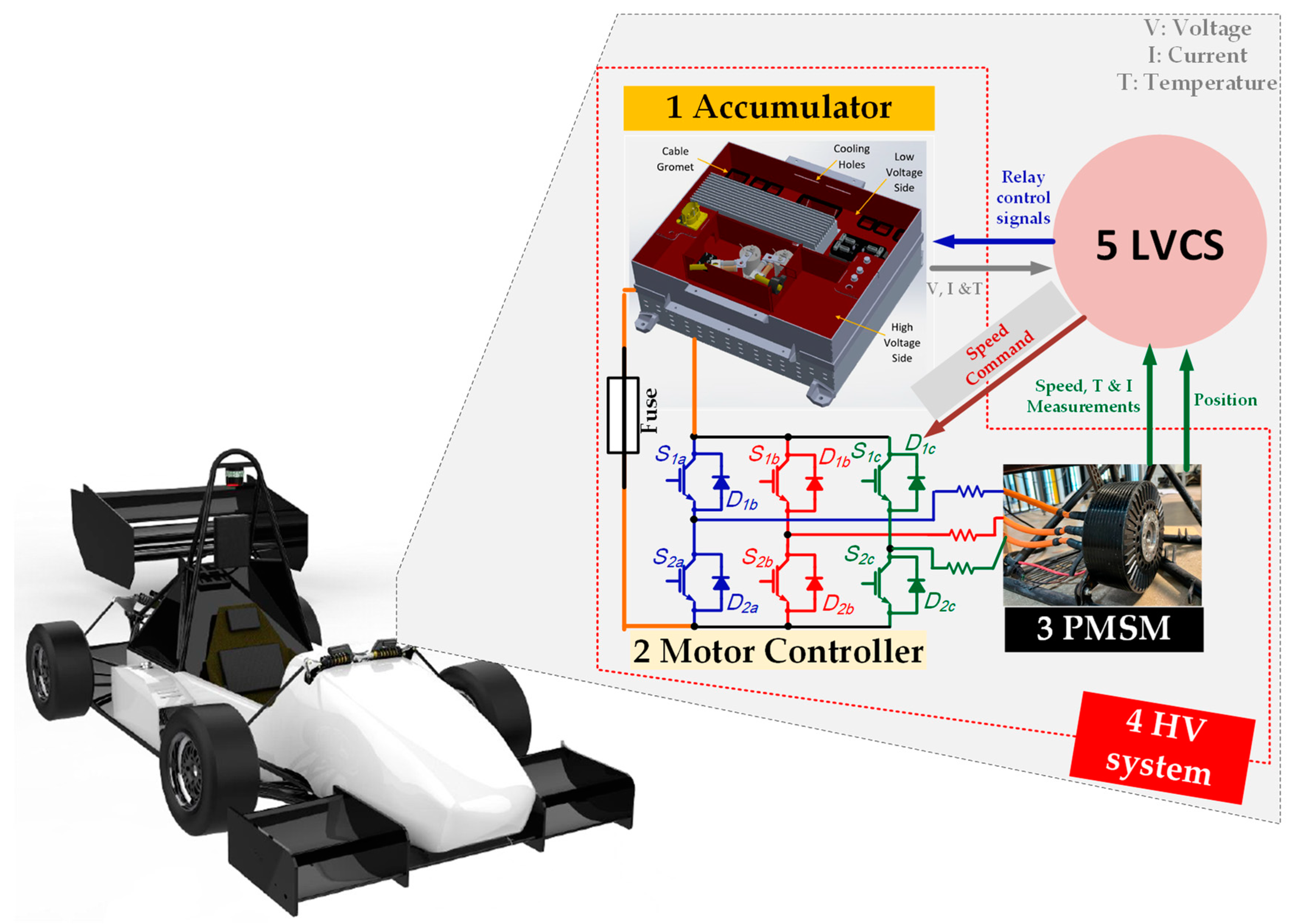
Figure 1. Main electrical systems of the FSERC.
Hardware 02 00010 g001
Figure 2. Schematic of the SD line.
Hardware 02 00010 g002
Figure 3. Electric motor circuit.
Hardware 02 00010 g003
Figure 4. Hard braking of the FSERC motor at t = 8 s.
Hardware 02 00010 g004
Figure 5. PMSM developed torque during hard braking.
Hardware 02 00010 g005
Figure 6. PMSM speed during hard braking.
Hardware 02 00010 g006
Figure 7. PMSM power during braking.
Hardware 02 00010 g007
Figure 8. BSPD EC logic.
Hardware 02 00010 g008
Figure 9. IMD/BMS ECs logic.
Hardware 02 00010 g009
Figure 10. SSD schematic.
Hardware 02 00010 g010
Figure 11. AIRs and pre-charge relay circuit.
Hardware 02 00010 g011
Figure 12. Pre-charge logic in the PDAL: (a) DC-link voltage and (b) pre-charge logic.
Hardware 02 00010 g012
Figure 13. Discharge logic in the PDAL.
Hardware 02 00010 g013
Figure 14. A simple logic diagram for the AL sub-circuit.
Hardware 02 00010 g014
Figure 15. TSAL beacon: (a) assembly and (b) bottom section.
Hardware 02 00010 g015
Figure 16. PDB connection between the accumulator and the LV system.
Hardware 02 00010 g016
Figure 17. Isolated DC/DC converter in the PDB.
Hardware 02 00010 g017
Figure 18. ECU block diagram.
Hardware 02 00010 g018
Figure 19. A simplified schematic of the BSPD circuit.
Hardware 02 00010 g019
Figure 20. BSPD stages: (a) fail check, (b) trigger check, and (c) power/delay.
Hardware 02 00010 g020aHardware 02 00010 g020b
Figure 21. A simplified schematic of the SSD circuit.
Hardware 02 00010 g021
Figure 22. SSD: (a) main control section, and (b) modular power stage.
Hardware 02 00010 g022
Figure 23. Main stages of the PDAL EC: (a) activation logic input, (b) capacitor charging and latching, (c) latching threshold calculation, (d) turn off threshold calculation, and (e) DC-link voltage comparison with the battery voltage.
Hardware 02 00010 g023aHardware 02 00010 g023b
Figure 24. Main stages of the TSAL EC: (a) Green light control and (b) plausibility check.
Hardware 02 00010 g024
Figure 25. PDB EC.
Figure 25. PDB EC.
Hardware 02 00010 g025
Figure 26. BSPD PCB.
Hardware 02 00010 g026
Figure 27. SSD PCB.
Figure 27. SSD PCB.
Hardware 02 00010 g027
Figure 28. PDAL PCB: (a) top part and (b) bottom part.
Hardware 02 00010 g028
Figure 29. TSAL PCB.
Hardware 02 00010 g029
Figure 30. PDB PCB.
Figure 30. PDB PCB.
Hardware 02 00010 g030
Figure 31. ECU: (a) PCB with Nucleo-F303RE Board and (b) without the MC.
Hardware 02 00010 g031aHardware 02 00010 g031b
Figure 32. Block diagram of the LVCS connection.
Hardware 02 00010 g032
Figure 33. BSPD test.
Hardware 02 00010 g033
Figure 34. SSD test.
Hardware 02 00010 g034
Figure 35. PDAL test during turning on the TS.
Hardware 02 00010 g035
Figure 36. PDAL test during turning off the TS.
Hardware 02 00010 g036
Figure 37. PDAL trips the TS due to an AMS error.
Hardware 02 00010 g037
Figure 38. TSAL green and red lights inspection.
Hardware 02 00010 g038
Figure 39. LVB discharge.
Hardware 02 00010 g039
Figure 40. PDB EC activation.
Hardware 02 00010 g040
Table 1. System paramater values in the MATLAB simulations.
ParamaterValue
Nominal DC-link voltage400 V
MotorPMSM
No. of poles10
Motor phase inductanceLd = Lq = 0.28 mH
Motor phase resistanceRs = 0.2 Ω
EV mass300 kg
Differential ratio1:4
Wheel radiusr = 30 cm
Table 2. Truth table for the TSAL inputs and outputs.
IntentionalActualResults in
Discrepancy
Voltage Measure
>60
Green LightRed Light
AIR 2AIR 1PREAIR 2AIR 1PRE
00000000ONOFF
××0××11×OFFLatch
×0××1×1×OFFLatch
0××1××1×OFFLatch
××1××01×OFFLatch
×1××0×1×OFFLatch
1××0××1×OFFLatch
××××××01OFFFlashing
1××1××0×OFFFlashing
×1××1×0×OFFFlashing
××1××10×OFFFlashing
0: OFF state; 1: ON state; ×: Can be both ON and/or OFF states.
Table 3. Main components of the BSPD EC.
ComponentPart No.Description
U2, U3, U4, U5, U9MCP6541Push-Pull Output Sub-Microamp Comparators
U7 and U8SN54HC324-channel, 2-input 2–6 V OR gate
U6TC74HC08AQuad 2-Input AND Gate
U11 4N35Optocoupler with Phototransistor Output
Q1PJA340430 V N-Channel Enhancement Mode MOSFET
K1653-G5Q-1A-HADC12General Purpose PCB Power Relay Mini 1-pole 10A
Table 4. Main components of the SSD EC.
ComponentPart No.Description
Q1, Q3, Q5,Q7MMBT3904VLNPN switching transistor
Q2, Q4, Q6, Q8RSD160P0545 V Drive P-channel MOSFET
Q9,Q10 H6327P-Ch −20 V MOSFET −630 mA
K1653-G5Q-1A-HADC12General Purpose PCB Relay Mini 1-pole 10 A
Table 5. Main components of the PDAL EC.
ComponentPart No.Description
K1OSA-SH-224DMGeneral Purpose PCB Relay
K2, K3653-G5Q-1A-HADC12General Purpose Power Relay Mini 1-pole 10 A
Q1–Q5PJA340430 V N-Channel Enhancement Mode MOSFET
U1–U4MCP6541Push-Pull Output Sub-Microamp Comparators
U5LT1086CT-12Low Dropout Positive 12 V/5 V Regulator
U6TC74HC08AQUAD 2-INPUT AND GATE
Table 6. Main components of the TSAL EC.
ComponentPart No.Description
U15, U18SFH617APhototransistor Output Optocoupler, Through Hole, 4-Pin DIP
K1, K2653-G5Q-1A-HADC12General Purpose Power Relay Mini 1-pole 10 A
Q1, Q2, Q4, Q6, Q7, Q8PJA340430 V N-Channel Enhancement Mode MOSFET
Q3, Q5RSD160P0545 V Drive P-channel MOSFET
U1–U3MCP6541Push-Pull Output Sub-Microamp Comparators
U13NCV7805BDTRKGLinear Voltage Regulator 700 mA, 5 V
U6SN74HC08NDual 4-Input AND Gate
Table 7. Main components of the PDB EC.
ComponentPart No.Description
K1653-G5Q-1A-HADC12General Purpose Power Relay 1-pole 10 A
U1DHS250B15400 V/12 V Isolated DC-DC Converter
U24N35Phototransistor Optocoupler
Table 8. Main components of the ECU EC.
ComponentPart No.Description
U1F303RESTM32F303RET6 microcontroller 3.6 V—72 MHz—51 GPIO
U2MCP2551-I/SNCAN Transceiver 1Mbps, 8-Pin
U3, U4, U5, U6EL8174 PIN DIP PHOTOTRANSISTOR PHOTOCOUPLER
U7TC74HC08AQuad 2-Input AND Gate
Q1, Q2PJA340430 V N-Channel Enhancement Mode MOSFET
Disclaimer/Publisher’s Note: The statements, opinions and data contained in all publications are solely those of the individual author(s) and contributor(s) and not of MDPI and/or the editor(s). MDPI and/or the editor(s) disclaim responsibility for any injury to people or property resulting from any ideas, methods, instructions or products referred to in the content.