Proceeding Paper

Two-Scale Deep Learning Model for Polysilicon MEMS Sensors †

by
José Pablo Quesada-Molina
1,2,* and
Stefano Mariani
1
1
Department of Civil and Environmental Engineering, Politecnico di Milano, Piazza Leonardo da Vinci 32, 20133 Milano, Italy
2
Department of Mechanical Engineering, Universidad de Costa Rica, San Pedro de Montes de Oca, 11501-2060 San José, Costa Rica
*
Author to whom correspondence should be addressed.
Presented at the 1st International Electronic Conference on Algorithms, 27 September–10 October 2021; Available online: https://ioca2021.sciforum.net/.
Comput. Sci. Math. Forum 2022, 2(1), 12; https://doi.org/10.3390/IOCA2021-10888
Published: 22 September 2021
(This article belongs to the Proceedings of The 1st International Electronic Conference on Algorithms)

Abstract

:
Microelectromechanical systems (MEMS) are often affected in their operational environment by different physical phenomena, each one possibly occurring at different length and time scales. Data-driven formulations can then be helpful to deal with such complexity in their modeling. By referring to a single-axis Lorentz force micro-magnetometer, characterized by a current flowing inside slender mechanical parts so that the system can be driven into resonance, it has been shown that the sensitivity to the magnetic field may become largely enhanced through proper (topology) optimization strategies. In our previous work, a reduced-order physical model for the movable structure was developed; such a model-based approach did not account for all the stochastic effects leading to the measured scattering in the experimental data. A new formulation is here proposed, resting on a two-scale deep learning model designed as follows: at the material level, a deep neural network is used a priori to learn the scattering in the mechanical properties of polysilicon induced by its morphology; at the device level, a further deep neural network is used to account for the effects on the response induced by etch defects, learning on-the-fly relevant geometric features of the movable parts. Some preliminary results are here reported, and the capabilities of the learning models at the two length scales are discussed.

1. Introduction

In recent years, the development of affordable and highly specialized hardware, designed to optimize large data computations via parallel processing [1,2] has propelled the widespread use of data-driven algorithms, such as machine learning (ML). This paradigm is revolutionizing the approach to the research activity in numerous areas, including the field of materials science [3,4,5].
The most popular types of ML algorithms are the artificial neural networks (ANNs). In their simplest modern form, feedforward neural networks (FFNNs) [6,7] are obtained by assembling a number of layers of interconnected perceptrons [8]. This architecture is typically referred to as the multilayer perceptron (MLP). By stacking a large enough number of layers, we enter into the realm of deep learning (DL), a subfield of ML that leverages the use of many levels of non-linear information processing and abstraction to produce complex learning tasks from unstructured input information [9]. In this context, a popular subtype of ANNs are the convolutional neural networks (CNNs). CNNs are well suited for input data featuring spatial correlation [10]; CNNs are able to learn position and scale invariant structures in the data. This aspect makes CNNs particularly efficient for tasks that rely upon auto-correlated and sequent data analysis, such as image recognition in computer vision, time series forecasting, or speech recognition in natural language processing. In the field of materials science, a significant number of CNN applications can be found in areas, such as material texture recognition [11,12,13,14] and structure to property mapping [15,16,17,18,19].
In this work, we propose a ML approach based in the implementation of an assemble of ANN architectures, to produce an accurate mapping between the structure of a polysilicon microelectromechanical system (MEMS) device and its effective response. We consider the Lorentz force MEMS magnetometer introduced in [20,21], and propose a new formulation resting on a two-scale deep learning model designed as follows: at the material level, a deep neural network is used a priori to learn the scattering in the mechanical properties of polysilicon induced by its morphology; at the device level, a further deep neural network is used to account for the effects on the response induced by etch defects, learning on-the-fly relevant geometric features of the movable parts. Hence, material- and geometry-related uncertainty sources, whose effects have been formerly studied and observed to intensify with the reduction in the size [22,23,24,25,26,27], are accounted for in this formulation. In concrete terms, the response is characterized in terms of the maximum oscillation amplitude of the resonant structure, a significant design parameter due to its direct relation with relevant figures of merit of the entire device, such as the responsivity and resolution [28]. The ground-truth data; required for the training, validation and testing of the proposed data-driven model, are obtained via the reduced-order model derived in [20,21].
The remainder of this work is organized as follows. The model of the polysilicon Lorentz force MEMS magnetometer and the intrinsic uncertainty sources at the microscale, are discussed in Section 2. Section 3 provides the methodology adopted for the implementation of the neural network-based model. Results are reported and analyzed in Section 4. Finally, concluding remarks and insights for future research work are collected in Section 5.

2. Model of the Polysilicon MEMS and Intrinsic Uncertainties

2.1. Oscillation Amplitude of the Lorentz Force MEMS Magnetometer

Within the various approaches to magnetic sensing [29], Lorentz force MEMS sensors operate by detecting effects of the Lorentz force, acting on a current-carrying conductor immersed into the magnetic field. The device is able to sense a magnetic field aligned with the out-of-plane direction z, see Figure 1, through the measurement of the in-plane motion of the beam. In the sketch, g is the gap between the two surfaces of parallel-plate capacitors (for sensing purposes), h is the in-plane width, and L the overall length of the flexible beam. The out-of-plane thickness is denoted by b, so that the area of the rectangular cross section is given by A = bh, and the moment of inertia is I = (bh3)/12. The beam is made of a polycrystalline silicon film with columnar structure, and the elastic properties governing its in-plane vibrations are assumed to be obtained through homogenization over a statistical volume element (SVE) of the polysilicon film.
During the operation, the mechanical structure is driven into resonance in order to obtain the maximum output signal. Larger vibration amplitudes are linked to higher responsivity and, therefore, better resolution. Neglecting a sequence of derivation steps (interested readers can find them in [20,21]), the maximum amplitude of the oscillations at the mid-span cross-section, ν m a x , is obtained as the solution of the following equation:
( F 0 K 1 ) = (   2 ( 1 ω ω 1 ) ν m a x + 3 4 K 3 K 1 ν m a x 3 ) 2 + (   d m ω 1 ν m a x ) 2
Terms in Equation (1) represent the effective mass (m), air damping (d), linear and cubic stiffnesses (K1 and K3), amplitude of the oscillating external Lorentz force ( F 0 ), frequency of the forcing term (ω), and natural frequency of the beam ( ω 1 ). The dynamics of this system is governed by weakly coupled thermo-electro-magneto-mechanical multi-physics, noticeable when writing explicit expressions for each of the previous terms. Nonetheless, the key aspect to highlight is that, since the solution for ν m a x depends on K1 and K3 which, in turn, depend on the flexural (EI) and axial (EA) rigidities of the beam, uncertainties in the values of the homogenized Young’s modulus, E ¯ and in-plane width, h (induced by defects such as over-etch, O), produce a scattering in the expected value of ν m a x .

2.2. Sources of Uncertainty in Polysilicon MEMS

Successful incorporation of MEMS-based products to market, hinges on the ability to engineer these components to have sufficient reliability for the intended applications [30]. Therefore, efforts to characterize the small-scale and scale-specific properties of materials are significantly driven by the need to predict the performance of MEMS and other microscale devices [31]. Manufacturing processes of MEMS are typically subjected to limited repeatability, impeding to obtain deterministic nominal geometries and material properties, which are instead characterized by a scattering around these values [32].
For the particular case of polysilicon-based MEMS, two main sources of uncertainty have been observed to intensify with the miniaturization of the devices [22,23,24,25,26,27]. The first source is related to the limits of the production process, i.e., when the size of the MEMS is in the same order of magnitude of the tolerances established by the microfabrication process. The second source is instead associated with the intrinsic heterogeneity of the material, i.e., when the size of the MEMS is in the same order of magnitude of the characteristic length of heterogeneities present in the material (for example the grain size in the case of polycrystalline materials). Since both sources of uncertainty are governed by variables that are stochastic in nature, statistical approaches need to be adopted to quantify their impact on the final properties. In practice, the effects of the first uncertainty type can be accounted for in terms of a defect parameter called over-etch depth O, while those associated with the second uncertainty type can be accounted in terms of the scattering observed in the apparent elastic properties (e.g., the homogenized Young’s modulus E ¯ ).
By following the procedure proposed in [22], it is possible to characterize the scattering of the homogenized in-plane Young’s modulus for SVEs of polysilicon films featuring different sizes, i.e., h = {2, 5} μm. Size-dependent statistics have been found to be well fitted by lognormal distributions and the relevant parameters are reported in Table 1.
On the other hand, geometry related uncertainties can be handled in accordance with former studies [23,25], wherein the over-etch depth O was sampled out of a microfabrication-tailored normal distribution featuring a zero mean μ and a standard deviation σ = 0.05 μm. Therefore, assuming O to be homogeneously distributed, it changes the in-plane film width according to h − 2O (h represents only a target size); accordingly, the cross-sectional area A of the beam is affected linearly by O, whereas the moment of inertia I is affected cubically. The gap at the capacitors is also modified as g + 2O, where g again represents a target size.

3. Methodology

3.1. Representation of the Resonant Structure

The resonant structure is considered as a concatenation of squared SVEs. These SEM-like subdomains are digitally generated via the regularized Voronoi tessellation procedure, such as described in [22]. These input images are characterized by two different target in-plane widths, h = 2 μm and 5 μm.
Given the symmetry displayed by the elastic properties as a function of the orientation in a silicon (1 0 0) wafer, see [33], the Young’s modulus of the monocrystalline domains remains invariant under a series of similarity transformations. This particularity motivated a data augmentation (D.A.) procedure wherein, for each original or parent SVE, seven new instances are generated, all linked to the same ground-truth value of the parent. The resonant structure is then regarded as a random concatenation (in space and frequency) of a parent SVE and its corresponding instances. Figure 2 illustrates these aspects.
The specific similarity transformations used for the D.A. procedure were: three counterclockwise 90° rotations, and four mirror transformations (horizontal, vertical, and about the two diagonals). Moreover, the pixel values ranging from [0, 255] encode the in-plane lattice orientation angle displayed by each monocrystalline domain.

3.2. The Neural Network-Based Model

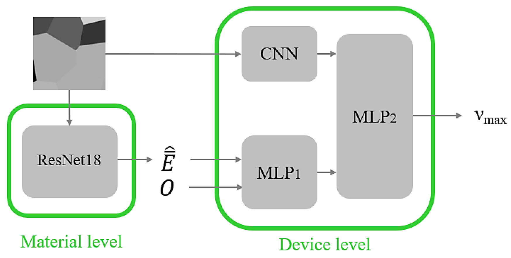
Starting with a general description of the neural network-based model, Figure 3 illustrates the overall model topology. Two stages can be distinguished in the proposed two-scale deep learning approach. At the material level (first stage), the digitally generated 128 × 128 pixels SVE images are fed to the ResNet-based model, developed in our former work [34], which is leveraged to provide the estimation of the homogenized in-plane Young’s modulus, E ¯ ^ . At the device level (second stage), the model takes the same SVE image (which is regarded as characteristic of the microstructure of the resonant structure), the estimated E ¯ ^ and an associated over-etch value, O (sampled from the relevant probability distribution described in Section 2.2). Differently from the first stage, the second stage handles multiple and mixed data type inputs. After training, the second stage learns to map from this input information to the maximum oscillation amplitude ν m a x , dealt with as the target variable of the entire model.
A detailed description of each of the components is presented hereafter. First, the ResNet-based regression leverages the use of residual learning [35] for a feature learning stage. Local and translational invariant low-level features, such as colors, edges, and shapes of the grains, are extracted in the initial convolutional layers. These features are then combined through further convolution operations in deeper layers, to achieve complex levels of abstraction and obtain high-level features, from which the model is ultimately able to produce the estimation of the homogenized in-plane Young’s modulus E ¯ ^ . More details about the training, validation, and testing process of this model can be found in [34].
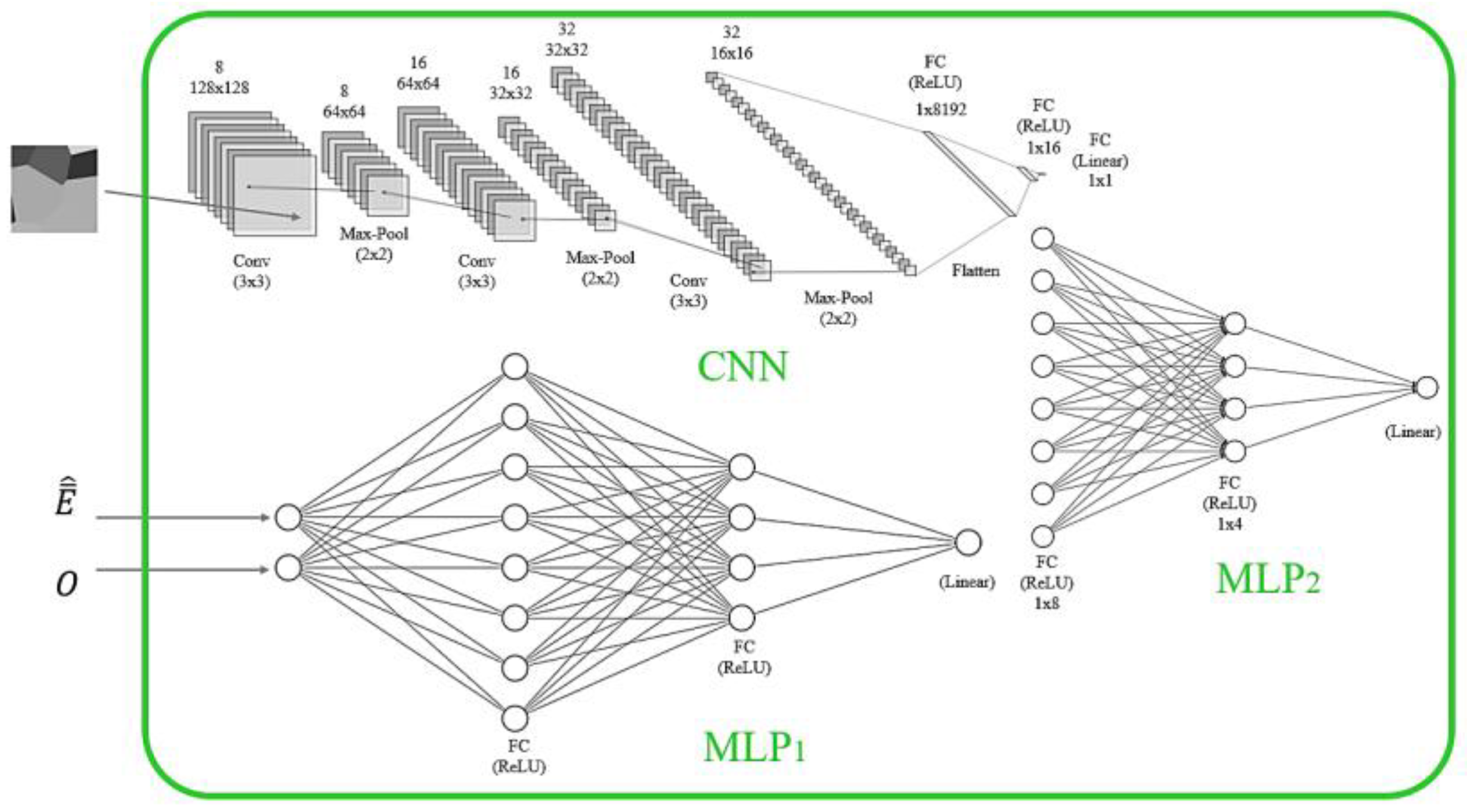
Figure 4 shows, in detail, the architectures used to learn the mapping at the device level. The single-neuron output layer of the CNN branch, and the single-neuron output layer of the MLP1 branch, are fully connected to the eight-neuron input layer of the MLP2.
The backbone of the CNN architecture employs a consecutive application of Convolution, ReLU activation, Batch Normalization, and Max-Pool operations. After the last Max-Pool layer, a flatten operation enables the connection of the feature extractor to a set of fully connected layers featuring a 16-node hidden layer and a 1-node output layer. For regularization purposes, dropout was applied to the 16-node hidden layer with a dropout rate of p = 0.5.
The MLP1 is composed of a sequence of fully connected layers. The specific sequence features an 8-node hidden layer followed by a 4-node and a 1-node output layer. As in the case of the CNN, only the output neuron was activated by a linear activation function while the rest of the units use ReLU activations. An identical configuration was chosen for MLP2.
Regarding the selection of hyperparameters, the total number of epochs was set to 1000, the patience (early stopping) to 100, the mini-batch size to 10, the learning rate α to 1 · 10−3, the optimizer to Adam and the loss function to MSE. Furthermore, the implementation was completed, making use of Keras API. Regarding the hardware, a GeForce GTX 1050 Ti GPU was used.
Concerning the data splitting, training, validation, and test sets were considered. Table 2 summarizes the information related to the number of samples and the statistics associated with the ground-truth values characterizing each set.

4. Results

We focus now on the results obtained with the second stage of the model, as related to the mapping of the maximum amplitude of oscillations performed at the device level. During the training, a minimum validation loss of 4.07 × 10⁻⁸  μ m2 was attained after 328 epochs. After this epoch, no considerable improvement was observed on the validation set over the next 100 epochs (set as the patience parameter), inducing the early stopping.
The parity plots in Figure 5 summarize the performance of the trained model over the training, validation, and test sets. These plots show the correlation between the predicted values of ν m a x obtained after the training of the model, and the corresponding ground-truth data provided by the reduced-order analytical model of the Lorentz force MEMS magnetometer (see Section 2.1). In black and grey, we can observe the mapping of the data associated with the 2 × 2   μ m2 and the 5 × 5   μ m2 SVEs, respectively. In light and dark green we have included the corresponding identity mapping, which represents the ideal behavior we could expect from the model.
As anticipated from the low loss values attained during the training, a very good agreement between predicted and ground-truth data is observed for all the sets and within each, for the two different in-plane widths handled for the SVE samples. To quantify this agreement, the coefficients of determination R2 are reported in the plots: R2 values are all close to 1, indicating a good performance. Moreover, as it could have been foreseen from the imbalance of the datasets, a slightly better result is observed for the smaller SVE samples.
In this work, the validation set has been employed, as conventionally, with the purpose of tuning the hyperparameters of the model during training. In order to assess the ability of the model to adapt to new, previously unseen data, drawn from the same distribution as the one used to train and tune the model, the performance over the test set can be analyzed. As can be observed in the parity plot, the predictions reproduce almost exactly the identity map. In terms of R2 values, the results are comparable to the performance obtained on the training set, which is a clear indication of the good generalization capability of the model.

5. Conclusions

A data-driven framework has been proposed and effectively implemented for modeling the response of a Lorentz force MEMS magnetometer. By enabling as input information, a digitally generated representative image of the microstructure together with a characteristic value for the over-etch O, the trained model has been able to produce accurate predictions of the maximum oscillation amplitude of the resonant structure. Moreover, the neural network-based model has been able to generalize satisfactorily over unseen samples drawn from the same distribution of the training data.
Future research activities will be oriented to incorporate the complete representation of the microstructure of the resonant structure, avoiding the introduced approximation of it as a random concatenation of an individual SVE and its instances obtained via D.A. An additional homogenization procedure is, therefore, foreseen, to upscale the Young’s modulus from the scale of the SVE to the scale of the resonant structure.
The implementation of an additional neural network is also envisioned, to achieve automatic defect detection, enabling O to be directly extracted from defect-informed digitally generated images of the microstructure.

Author Contributions

Conceptualization, J.P.Q.-M. and S.M.; methodology, J.P.Q.-M. and S.M.; software, J.P.Q.-M. and S.M.; validation, J.P.Q.-M. and S.M.; formal analysis, J.P.Q.-M. and S.M.; investigation, J.P.Q.-M. and S.M.; resources, J.P.Q.-M. and S.M.; data curation, J.P.Q.-M. and S.M.; writing—original draft preparation, J.P.Q.-M. and S.M.; writing—review and editing, J.P.Q.-M. and S.M.; visualization, J.P.Q.-M. and S.M.; supervision, J.P.Q.-M. and S.M.; project administration, J.P.Q.-M. and S.M.; funding acquisition, J.P.Q.-M. and S.M. All authors have read and agreed to the published version of the manuscript.

Funding

This research received no external funding.

Institutional Review Board Statement

Not applicable.

Informed Consent Statement

Not applicable.

Data Availability Statement

Not applicable.

Acknowledgments

JPQM acknowledges the financial support by Universidad de Costa Rica, to pursue postgraduate studies abroad.

Conflicts of Interest

The authors declare no conflict of interest.

References

  1. Owens, J.D.; Houston, M.; Luebke, D.; Green, S.; Stone, J.E.; Phillips, J.C. GPU Computing. Proc. IEEE 2008, 96, 879–899. [Google Scholar] [CrossRef]
  2. Nickolls, J.; Dally, W.J. The GPU Computing Era. IEEE Micro 2010, 30, 56–69. [Google Scholar] [CrossRef]
  3. Schmidt, J.; Marques, M.R.G.; Botti, S.; Marques, M.A.L. Recent advances and applications of machine learning in solid-state materials science. NPJ Comput. Mater. 2019, 5, 83. [Google Scholar] [CrossRef]
  4. Himanen, L.; Geurts, A.; Foster, A.S.; Rinke, P. Data-Driven Materials Science: Status, Challenges, and Perspectives. Adv. Sci. 2019, 6, 1900808. [Google Scholar] [CrossRef] [PubMed]
  5. Bock, F.E.; Aydin, R.C.; Cyron, C.J.; Huber, N.; Kalidindi, S.R.; Klusemann, B. A Review of the Application of Machine Learning and Data Mining Approaches in Continuum Materials Mechanics. Front. Mater. 2019, 6, 110. [Google Scholar] [CrossRef] [Green Version]
  6. Haykin, S. Neural Networks: A Comprehensive Foundation, 2nd ed.; Prentice Hall: Upper Saddle River, NJ, USA, 1998. [Google Scholar]
  7. Russell, S.J.; Norvig, P. Artificial Intelligence: A Modern Approach, 1st ed.; Pearson Education Limited: Kuala Lumpur, Malaysia, 2016. [Google Scholar]
  8. Rosenblatt, F. The perceptron: A probabilistic model for information storage and organization in the brain. Psych. Rev. 1958, 65, 386–408. [Google Scholar] [CrossRef] [PubMed] [Green Version]
  9. Deng, L. Deep Learning: Methods and Applications. FNT Signal Processing 2014, 7, 197–387. [Google Scholar] [CrossRef] [Green Version]
  10. Schmidhuber, J. Deep learning in neural networks: An overview. Neural Netw. 2015, 61, 85–117. [Google Scholar] [CrossRef] [Green Version]
  11. Cang, R.; Ren, M.Y. Deep Network-Based Feature Extraction and Reconstruction of Complex Material Microstructures. In Proceedings of the 42nd Design Automation Conference, Charlotte, NC, USA, 21–24 August 2016; American Society of Mechanical Engineers: New York, NY, USA, 2016. [Google Scholar] [CrossRef]
  12. Lubbers, N.; Lookman, T.; Barros, K. Inferring low-dimensional microstructure representations using convolutional neural networks. Phys. Rev. E 2017, 96, 052111. [Google Scholar] [CrossRef] [Green Version]
  13. Napoletano, P.; Piccoli, F.; Schettini, R. Anomaly Detection in Nanofibrous Materials by CNN-Based Self-Similarity. Sensors 2018, 18, 209. [Google Scholar] [CrossRef] [Green Version]
  14. Hwang, H.; Oh, J.; Lee, K.-H.; Cha, J.-H.; Choi, E.; Yoon, Y.; Hwang, J.-H. Synergistic approach to quantifying information on a crack-based network in loess/water material composites using deep learning and network science. Comp. Mat. Sci. 2019, 166, 240–250. [Google Scholar] [CrossRef]
  15. Yang, Z.; Yabansu, Y.C.; Al-Bahrani, R.; Liao, W.; Choudhary, A.N.; Kalidindi, S.R.; Agrawal, A. Deep learning approaches for mining structure-property linkages in high contrast composites from simulation datasets. Comp. Mat. Sci. 2018, 151, 278–287. [Google Scholar] [CrossRef]
  16. Cecen, A.; Dai, H.; Yabansu, Y.C.; Kalidindi, S.R.; Song, L. Material structure-property linkages using three-dimensional convolutional neural networks. Acta Materialia. 2018, 146, 76–84. [Google Scholar] [CrossRef]
  17. Cang, R.; Li, H.; Yao, H.; Jiao, Y.; Ren, Y. Improving direct physical properties prediction of heterogeneous materials from imaging data via convolutional neural network and a morphology-aware generative model. Comp. Mat. Sci. 2018, 150, 212–221. [Google Scholar] [CrossRef] [Green Version]
  18. Frankel, A.L.; Jones, R.E.; Alleman, C.; Templeton, J.A. Predicting the mechanical response of oligocrystals with deep learning. Comp. Mat. Sci. 2019, 169, 109099. [Google Scholar] [CrossRef] [Green Version]
  19. Abueidda, D.W.; Almasri, M.; Ammourah, R.; Ravaioli, U.; Jasiuk, I.M.; Sobh, N.A. Prediction and optimization of mechanical properties of composites using convolutional neural networks. Comp. Struct. 2019, 227, 111264. [Google Scholar] [CrossRef] [Green Version]
  20. Bagherinia, M.; Bruggi, M.; Corigliano, A.; Mariani, S.; Lasalandra, E. Geometry optimization of a Lorentz force, resonating MEMS magnetometer. Micro. Rel. 2014, 54, 1192–1199. [Google Scholar] [CrossRef]
  21. Bagherinia, M.; Mariani, S. Stochastic Effects on the Dynamics of the Resonant Structure of a Lorentz Force MEMS Magnetometer. Actuators 2019, 8, 36. [Google Scholar] [CrossRef] [Green Version]
  22. Mariani, S.; Martini, R.; Ghisi, A.; Corigliano, A.; Beghi, M. Overall elastic properties of polysilicon films: A statistical investigation of the effects of polycrystal morphology. Int. J. Mult. Comp. Eng. 2011, 9, 327–346. [Google Scholar] [CrossRef]
  23. Mirzazadeh, R.; Mariani, S. Uncertainty Quantification of Microstructure-Governed Properties of Polysilicon MEMS. Micromachines 2017, 8, 248. [Google Scholar] [CrossRef] [Green Version]
  24. Mariani, S.; Ghisi, A.; Mirzazadeh, R.; Azam, S.E. On-Chip Testing: A Miniaturized Lab to Assess Sub-Micron Uncertainties in Polysilicon MEMS. Micro Nanosyst. 2018, 10, 84–93. [Google Scholar] [CrossRef]
  25. Mirzazadeh, R.; Eftekhar Azam, S.; Mariani, S. Mechanical Characterization of Polysilicon MEMS: A Hybrid TMCMC/POD-Kriging Approach. Sensors 2018, 18, 1243. [Google Scholar] [CrossRef] [PubMed] [Green Version]
  26. Ghisi, A.; Mariani, S. Effect of Imperfections Due to Material Heterogeneity on the Offset of Polysilicon MEMS Structures. Sensors 2019, 19, 3256. [Google Scholar] [CrossRef] [PubMed] [Green Version]
  27. Dassi, L.; Merola, M.; Riva, E.; Santalucia, A.; Venturelli, A.; Ghisi, A.; Mariani, S. A Stochastic Model to Describe the Scattering in the Response of Polysilicon MEMS. Eng. Proc. 2021, 2, 95. [Google Scholar] [CrossRef]
  28. Herrera-May, A.; Soler-Balcazar, J.; Vázquez-Leal, H.; Martínez-Castillo, J.; Vigueras-Zuñiga, M.; Aguilera-Cortés, L. Recent Advances of MEMS Resonators for Lorentz Force Based Magnetic Field Sensors: Design, Applications and Challenges. Sensors 2016, 16, 1359. [Google Scholar] [CrossRef] [PubMed] [Green Version]
  29. Lenz, J.; Edelstein, S. Magnetic sensors and their applications. IEEE Sens. J. 2006, 6, 631–649. [Google Scholar] [CrossRef]
  30. Hartzell, A.; Silva, M.; Shea, H. MEMs Reliability, 1st ed.; Springer: Berlin/Heidelberg, Germany, 2011. [Google Scholar] [CrossRef]
  31. Hemker, K.J.; Sharpe, W.N., Jr. Microscale Characterization of Mechanical Properties. Annu. Rev. Mater. Res. 2007, 37, 93–126. [Google Scholar] [CrossRef]
  32. Uhl, T.; Martowicz, A.; Codreanu, I.; Klepka, A. Analysis of uncertainties in MEMS and their influence on dynamic properties. Arch. Mech. 2009, 61, 349–370. [Google Scholar]
  33. Hopcroft, M.A.; Nix, W.D.; Kenny, T.W. What is the Young’s Modulus of Silicon? J. Micro. Syst. 2010, 19, 229–238. [Google Scholar] [CrossRef] [Green Version]
  34. Quesada-Molina, J.P.; Rosafalco, L.; Mariani, S. Mechanical Characterization of Polysilicon MEMS Devices: A Stochastic, Deep Learning-based Approach. In Proceedings of the 2020 21st International Conference on Thermal, Mechanical and Multi-Physics Simulation and Experiments in Microelectronics and Microsystems (EuroSimE), Cracow, Poland, 5–8 July 2020; IEEE: Piscataway, NJ, USA, 2020. [Google Scholar] [CrossRef]
  35. He, K.; Zhang, X.; Ren, S.; Sun, J. Deep Residual Learning for Image Recognition. In Proceedings of the 2016 IEEE Conference on Computer Vision and Pattern Recognition (CVPR), Las Vegas, NV, USA, 27–30 June 2016; IEEE: Piscataway, NJ, USA, 2016. [Google Scholar] [CrossRef] [Green Version]
Figure 1. (a) SEM picture of the resonant structure of the MEMS magnetometer [20]; (b) Scheme of the slender beam of length L. Parallel plates are connected to the mid-span of the beam for capacitive sensing [21].
Csmf 02 00012 g001
Figure 2. Example of parent SVE with h = 2 μm, its instances, and the resonant structure.
Csmf 02 00012 g002
Figure 3. Topology for the proposed data-driven model.
Csmf 02 00012 g003
Figure 4. Architectures of the model used for the mapping at the device level.
Csmf 02 00012 g004
Figure 5. Parity plots for the model at the device level: (a) Training set; (b) Validation set; (c) Test set.
Csmf 02 00012 g005
Table 1. Statistical indicators characterizing E ¯ for different SVE sizes, obtained with uniform strain boundary conditions.
SVE Sizeμ [GPa]σ [GPa]
2   μ m × 2   μ m150.15.5
5   μ m × 5   μ m149.32.4
Table 2. Data splitting information.
SizeSVEs Mean   ν m a x   [ μ m ] Standard   Deviation   ν m a x   [ μ m ]
Training2   μ m × 2   μ m18980.0280.004
5   μ m × 5   μ m8000.010.002
Validation2   μ m × 2   μ m4000.0280.004
5   μ m × 5   μ m2000.010.002
Test2   μ m × 2   μ m1980.0280.004
5   μ m × 5   μ m990.010.002
Publisher’s Note: MDPI stays neutral with regard to jurisdictional claims in published maps and institutional affiliations.