Article

Hardware-Described Nanoscale Carry-Save Adder in Quantum-Dot Cellular Automata: An Optimised Design and Evaluation Framework

by
Mohammad Abdullah-Al-Shafi
Faculty of Science and Engineering, Southern Cross University, Coolangatta, Gold Coast, QLD 4225, Australia
Chips 2025, 4(4), 43; https://doi.org/10.3390/chips4040043
Submission received: 15 August 2025 / Revised: 6 October 2025 / Accepted: 11 October 2025 / Published: 15 October 2025

Abstract

Quantum-dot Cellular Automata (QCA) technology has emerged as a promising approach for constructing nanoscale digital circuits, offering notable advantages such as minimal power consumption, rapid processing speeds, and highly compact layouts. Traditional CMOS technology faces significant challenges at the nanoscale, including reduced gate control and increased current leakage. QCA, on the other hand, provides a robust platform for building next-generation digital systems. In this study, a unique single-layer QCA-based Full-Adder (QCAFA) and Carry-Save Adder (CSA) architecture is developed to enhance key performance factors such as delay, space, cost, and cell block count. The outlined designs demonstrate superior efficiency compared to state-of-the-art single-layer and multilayer QCA designs. Simulation results conducted with QCADesigner 2.0.3 and QCADesigner-E reveal that the proposed architecture achieves a substantial 34.29% diminution in total cells compared with the recent design, utilising only 46 QCA cells. Similarly, for the CSA, the proposed design attains an 18.62% reduction in cell count compared with its best counterpart, utilising only 424 QCA cell blocks. To enhance design credibility and hardware relevance, this research additionally models and validates the architecture using the Verilog hardware description language (HDL Version 12.0), thereby bridging the gap between nano-architecture and HDL-based prototyping. Simulation results obtained through QCADesigner confirm the correctness and stability of the QCA layout, while HDL simulation verifies functional equivalence at the behavioural and structural levels. The proposed designs not only enhance speed and reduce energy consumption but also offer better manufacturability. The findings of this study highlight the potential of QCA technology as a feasible substitute for CMOS for high-performance digital arithmetic circuits at the nanoscale.

1. Introduction

Over the past decades, complementary metal–oxide–semiconductor (CMOS) technology has dominated digital system design owing to its scalability, robustness, and cost-effectiveness [1]. However, as transistor scaling approaches its physical and thermal boundaries, CMOS is increasingly constrained in delivering the speed, energy efficiency, and miniaturisation required by next-generation applications [2]. This technological bottleneck has accelerated the search for alternative paradigms capable of sustaining continued advancements in nanoelectronics. Quantum-dot Cellular Automata (QCA) has emerged as one of the most promising nanoscale architectures, offering a fundamentally different approach to digital circuit implementation [3]. Unlike CMOS, which relies on current conduction through transistors, QCA utilises the Coulombic interaction of electrons within quantum dots to encode and process binary information [4]. This unique operating principle provides substantial advantages, including ultra-low power consumption, high operating frequency, minimal delay, and an exceptionally compact device footprint [5,6]. Reports suggest that QCA can achieve energy efficiencies several orders of magnitude greater than the most advanced CMOS technologies [7], positioning it as a viable candidate for future ultra-efficient digital systems.
The design potential of QCA extends across combinational and sequential logic, with a wide range of implementations demonstrated, including logic gates [8,9,10,11,12,13,14,15,16,17,18,19,20,21], multiplexers [11], flip-flops [9,17,18], and arithmetic units [8,9,10,11,12,13,14,15,16,17,18,19,20,21]. Arithmetic circuits are of particular significance, as they form the foundation of complex computing structures such as multipliers and arithmetic logic units (ALUs) [15]. Within this domain, the full adder (QCAFA) and carry-save adder (CSA) have drawn considerable attention due to their direct impact on computational performance and energy efficiency. The QCAFA, as a fundamental arithmetic component, influences overall circuit complexity, area, and power dissipation [22], while the CSA is critical in accelerating the summation of multiple operands, an essential operation in high-performance computing [23].
In this study, the researcher presents novel designs for QCA-based full adders and carry-save adders optimised to reduce key performance costs, including cell count, layout area, and power dissipation, while improving overall computational efficiency. The proposed architecture covers the inherent intercellular interactions of QCA to achieve highly streamlined and scalable layouts. Circuit implementation is carried out using QCADesigner 2.0.3, with detailed energy dissipation analysis conducted via QCADesigner-E. A comprehensive comparative evaluation against state-of-the-art designs [23,24,25,26,27,28,29,30,31,32,33,34,35,36,37,38,39,40] highlights the superiority of the proposed schemes, offering valuable insights into their practicality, efficiency, and relevance for the next generation of nanoscale arithmetic architectures. While extensive research has been conducted on QCA adders, relatively little attention has been paid to combining QCA architecture with HDLs for hardware validation and prototyping [41]. Incorporating HDL modelling allows QCA designs to be verified within established digital design flows, ensuring compatibility with FPGA/ASIC toolchains and improving accessibility for designers [42]. This work proposes a QCA-based CSA architecture and presents its corresponding Verilog HDL model, establishing a framework that connects nanoscale device design with conventional digital hardware representation. This dual-layer approach enables both physical-level analysis through QCADesigner and functional-level verification via HDL simulation.
This paper is organised to guide the reader through both the foundations and innovations of the work. Section 2 introduces the fundamentals of QCA, outlining its governing principles and underlying operation. Section 3 surveys the latest advances in QCAFA and CSA, positioning the present study within the broader research landscape. Section 4 details the proposed designs, emphasising their structural efficiency and functional advantages. Section 5 delivers a rigorous comparative assessment, highlighting improvements across critical performance metrics, including cell complexity, resource utilisation, and computational delay. Finally, Section 6 concludes the study, distilling the key outcomes and pointing toward promising directions for future exploration in nanoscale circuit design.

2. Theoretical Foundations of Quantum-Dot Cellular Automata

QCA represents a transformative nanoscale computing paradigm in which each cell functions as a fundamental logic element. A typical QCA cell consists of four quantum dots arranged in a square configuration, hosting two electrons confined by Coulombic repulsion [43,44,45,46]. This electrostatic interaction produces two stable polarisation states, corresponding to binary values “0” and “1” [3,4]. Cells are conventionally illustrated as squares (Figure 1a), with their states regulated by potential barriers and synchronised by a multi-phase clocking system.
State transitions occur through quantum tunnelling of electrons between neighbouring dots. This process is inherently nonlinear, shaped both by internal electron interactions and by the electrostatic forces of adjacent cells [47]. As a result, the polarisation of a QCA cell is directly influenced by its nearest neighbours, enabling information transfer through cell-to-cell interaction [48]. Sequential alignment of cells forms QCA wires, which propagate binary signals from input to output via electrostatic coupling. Depending on orientation, wires are classified as 90° (orthogonal) or 45° (diagonal) structures (Figure 1b).
Two primary logic primitives underpin QCA circuit design. The majority voter (MV) gate, typically composed of three inputs, a device cell, and one output, determines its output polarisation according to the majority state of its inputs (Figure 1c) [8,9]. The inverter, or NOT gate, operates by arranging cells diagonally so that Coulombic repulsion forces opposite polarisations, achieving signal inversion (Figure 1d) [10,11].
A major challenge in QCA architecture is wire crossing, as improper design may cause interference or signal degradation [12,13]. Two key strategies address this. In multilayer crossovers, wires are placed on different physical layers, employing 90° cells with non-neighbouring clock phases to ensure interference-free transmission (Figure 1e) [15]. Coplanar crossovers, by contrast, permit intersections within the same plane, generally combining 45° and 90° cells to minimise disruption (Figure 1f) [16].
An alternative technique, logical crossing, eliminates structural overlaps. By carefully controlling clocking phases, signals can traverse one another within a single plane without mutual interference, offering an elegant and efficient crossover solution (Figure 1g) [8]. Another method was evaluated by eliminating the central cell at the wire-crossing region and systematically analysing the resulting signal behaviour. The detail of this method is described in [49].
An integral feature of QCA technology lies in its advanced clocking architecture, which not only directs the propagation of information but also preserves the stability of logic states within cells [15]. In contrast to traditional electronic circuits, QCA employs a four-phase clocking strategy that modulates potential barriers inside the cells while synchronising data flow throughout the circuit (Figure 1h) [19]. This cyclical mechanism operates through four distinct stages:
Switching Phase: Potential barriers are progressively raised, enabling the cell to align with the incoming logic state. By the end of this interval, the barriers reach a sufficiently high level to inhibit electron tunnelling, thereby locking the cell into a stable polarisation.
Holding Phase: With barriers maintained at their peak, the cell securely retains its state, ensuring reliable transmission of its logic value to neighbouring cells.
Releasing Phase: As the barriers begin to diminish, the stabilisation of the polarisation weakens, making the cell receptive to updated input signals.
Relaxation Phase: The barriers are fully lowered, effectively resetting the cell and erasing its prior state, thereby preparing it for the next clocking cycle.
Through this orchestrated sequence, the QCA clocking scheme delivers accurate data transfer, synchronisation, and directional control of signals within the circuit [20]. Crucially, it also establishes the flow of information, which is a decisive factor in the efficient design and implementation of complex QCA-based architectures [21]. In the proposed CSA design, the adder cells are organised into distinct clock zones that operate sequentially. In the CSA configuration, each input signal (x1–x4, y1–y4, z1–z4) enters through an assigned clock zone, and the generated intermediate outputs (s1–s6) are systematically propagated towards the final carry and sum outputs. This staggered arrangement ensures that outputs from one stage are correctly latched and stabilised before propagating to the next, achieving robust synchronisation across the entire adder. The careful assignment of clock phases minimises latency, preserves functional correctness, and enables the circuit to sustain scalability at the nanoscale. Thus, the integration of clocking and synchronisation is fundamental to the CSA’s reliable performance, ensuring that carry and sum signals are transmitted in a coordinated manner without timing hazards. This design consideration enhances both the computational accuracy and the overall stability of the architecture, particularly under nanoscale constraints.
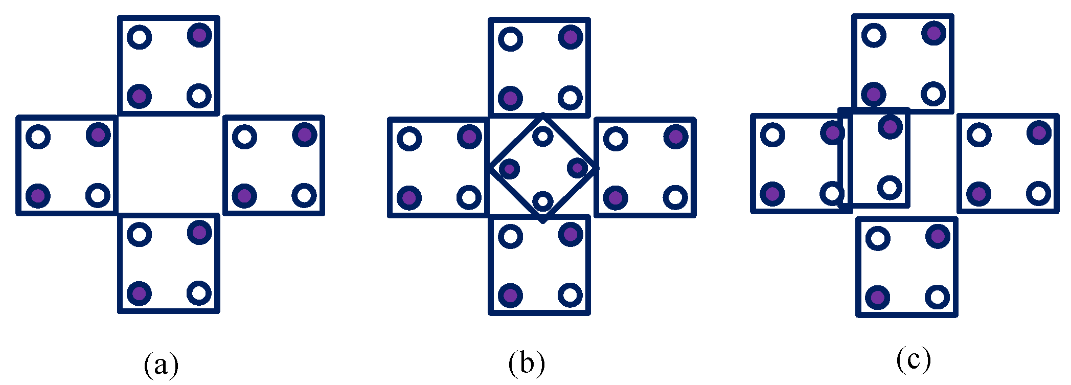
QCA circuit layouts are extremely sensitive to structural imperfections, with three fault types posing critical threats: missing cells, misaligned cells, and dislocated cells, as shown in Figure 2a–c.
A missing cell fault emerges when a cell block is absent, producing gaps that can quietly go unnoticed or, in worst-case scenarios, completely halt circuit operation.
Misaligned cell faults occur when cells are shifted from their intended positions; even minor deviations can cascade into unpredictable and erroneous behaviour [8].
The most perilous fault—a dislocated cell fault—arises when a cell block rotates to an improper orientation relative to its neighbours, disrupting signal flow and potentially triggering total circuit failure [8]. These vulnerabilities underscore the narrow margin for error in QCA design, where even subtle structural inconsistencies can compromise the integrity of nanoscale circuits.

3. Review of Existing Research and Developments

This section provides a comprehensive review of recent advancements in QCAFA and CSA designs, emphasising their key characteristics and identifying inherent limitations. Over the past several years, researchers have proposed diverse architectures aimed at enhancing the efficiency, speed, and area optimisation of QCA-based adder circuits [23,24,25,26,27,28,29,30,31,32,33,34,35,36,37,38,40]. While numerous designs exist, this study concentrates specifically on state-of-the-art contributions reported between 2018 and 2025. Focusing on this seven-year interval enables a meaningful evaluation of technological progress, capturing both well-established improvements and emerging innovations. By concentrating on contemporary designs, the analysis remains directly relevant to current fabrication technologies, advanced simulation methodologies, and the growing emphasis on energy-efficient nanoscale circuits. This targeted review not only underscores recent performance trends and design optimisations but also provides critical insights to guide the development of next-generation QCA adder architectures. For instance, Joy et al. [24] introduced a QCAFA comprising 64 cells, occupying 0.078 µm2 with a cell area of 0.024 µm2, achieving a resource cost of 0.035 and a latency of 1.25 clock cycles. Maharaj and Muthurathinam [25] proposed a slightly larger design with 93 cells, 0.087 µm2 area, 0.027 µm2 cell area, a resource cost of 0.087, and a latency of 2. Designs reported by Sasamal et al. [26] and Singhal [27] utilised even more cells-111 and 114, respectively, resulting in larger footprints of 0.13 µm2 and 0.23 µm2, cell areas of 0.040 µm2 and 0.071 µm2, resource costs of 0.9831 and 0.359, and latencies of 2.75 and 1.25. More compact designs have also been proposed. Raj et al. [28] presented a 75-cell QCAFA with an area of 0.09 µm2, cell area of 0.028 µm2, resource cost of 0.051, and latency of 0.75. XOR gate-based QCAFAs designed by Erniyazov and Jeon [29] and Wang and Xie [30] demonstrated further optimisation, employing 61 and 60 cells, with areas of 0.076 µm2 and 0.057 µm2, cell areas of 0.023 µm2 and 0.018 µm2, resource costs of 0.019 and 0.057, and latencies of 0.5 and 1, respectively. Similarly, Safoev [31] and Sarvaghad-Moghaddam [32] proposed highly efficient adders with 56 and 52 cells, areas of 0.047 µm2 and 0.038 µm2, cell areas of 0.015 µm2 and 0.012 µm2, resource costs of 0.047 and 0.023, and latencies of 1 and 0.75. Additional designs reported in [33,34,35,36] further illustrate trends toward minimisation, featuring 47, 44, 70, and 46 cells. Notably, the most compact design examined in this study utilises only 46 cells, occupying 0.04 µm2 with a cell area of 0.012 µm2, achieving a resource cost of merely 0.0025 and a latency of 0.25. Collectively, these findings reveal a clear trajectory toward reduced area, lower cell counts, and improved speed, highlighting the critical trade-offs between resource utilisation, latency, and circuit complexity in contemporary QCA adder designs.
Hasani and Navimipour [23] proposed a CSA comprising 347 cells, occupying an area of 0.37 µm2 with a cell spacing of 0.11 µm2, a resource cost of 1.87, and a latency of 2.25. While this design demonstrates considerable efficiency, it encounters latency limitations and relies on multilayer crossings. In contrast, De and Das [38] introduced a CSA with a markedly reduced quantum cost through a novel full-adder architecture based on five-input majority logic, forming the foundation for the CSA. Their design supports larger operands by cascading multiple CSAs into an adder tree, achieving lower cell counts and reduced latency relative to prior QCA full-adder implementations. Nevertheless, this approach demands a higher number of QCA cell blocks. Erniyazov and Jeon [29] proposed a single-layer full-adder design augmented with an inverter chain, which they extended to develop both carry-look-ahead and carry-save adders. By leveraging the intrinsic pipelining capabilities of QCA and the inverter series, their design minimises the overall area while enhancing energy efficiency and circuit density. Experimental evaluations indicate superior performance in terms of cell count, latency, and spatial efficiency, despite consuming 696 cell blocks, occupying 0.66 µm2 with 0.20 µm2 cell spacing, incurring a cost of 4.13, and exhibiting a latency of 2.50. Amiri et al. [40] reported a CSA design with 521 cells, covering 0.62 µm2, with 0.19 µm2 cell spacing, a cost of 1.90, and a latency of 1.75. Compared to the previously discussed designs, this implementation involves higher cell usage, area, cost, and latency. Walus et al. [45] presented a CSA comprising 815 cells, with an area of 0.738 µm2, cell spacing of 0.23 µm2, a cost of 11.81, and a latency of 4, effectively doubling the resources and delay relative to the proposed design. Pudi and Sridharan [46] focused on fundamental QCA components, such as majority gates and inverters, demonstrating that a 1-bit full adder can be efficiently implemented using only three majority gates and at most one inverter. They further proposed an optimised QCA architecture for various prefix adders and n-bit ripple carry adders, with simulation results indicating reduced delay and area compared to earlier designs. Their implementation occupies 698 cell blocks, with an area of 0.618 µm2, a 0.19 µm2 cell spacing, incurs a cost of 9.89, and exhibits a latency of 4. The CSA proposed in this work occupies a smaller area and requires fewer cell blocks than the designs presented in [23,29,38,40,45,46]. While the layout in [23] demonstrates competitive performance across several parameters, it suffers from multilayer complexity. The improvements of the current design are achieved through area-efficient adder architecture, which enhances operating speed while minimising spatial requirements. Moreover, the proposed CSA surpasses previous models in key performance metrics, including cell count and latency, resulting in a substantially reduced overall cost relative to prior implementations.

4. Design and Development of the Proposed QCAFA and CSA

Binary addition constitutes a primary arithmetic function within the domain of digital computation, underpinning the architecture of a wide array of processing units. The implementation of this function is achieved through adder circuits, which are therefore integral to the construction of any arithmetic logic unit (ALU). Herein, the study details a proposed full-adder cell, characterised by its three input ports (x, y, z) and two output ports, sum (s) and carry (c). The output logic for this cell is explicitly modelled by the mathematical expressions presented in Equations (1) and (2).
sum = mv   ( mv   ( x ,   y ¯ ,   z ) ,   mv   ( x ,   y ,   z ¯ ) ,   mv   ( x ¯ ,   y ,   z ) )
carry = mv (x, y, z)
In the above calculations, mv can signify either a three-input or five-input majority voter. This majority logic is instrumental in the architecture of the proposed QCAFA, a circuit engineered to compute the sum (s) and carry (c) for each bit position in a binary addition operation. The QCAFA accepts a triplet of inputs: xi and yi (the nth bits of the addends) and zi (the carry-in from the lower-order bit). As formalised by the Boolean functions in Equations (3) and (4), the carry output is generated directly and efficiently by the majority gate. Conversely, the sum output is synthesised through a more elaborate assembly of inverters and majority gates, a configuration that inherently requires further optimisation to minimise latency and maximise computational throughput.
s n = x n     y n     z n
cn + 1 = xnyn + xnzn + ynzn
The functional integrity and performance of the proposed QCAFA were rigorously validated using the QCADesigner 2.0.3 simulation environment, a robust platform for the design and testing of QCA circuits. Within this suite, the bistable approximation engine was employed over the coherence vector approach, primarily for its superior computational speed, which facilitates rapid design iteration and verification. The logical architecture of the QCAFA, a one-bit full adder, is delineated by the truth function presented in Table 1. As illustrated in the schematic layout (Figure 3a), the circuit processes two one-bit inputs, x and y, along with a carry-in bit, z, to generate a sum (s) and a carry-out (c). The proposed architecture is remarkably compact, comprising 46 QCA cells and requiring a complete propagation sequence of clock cycles to generate the final outputs. The simulation waveforms, depicted in Figure 3b, corroborate the circuit’s correct logical operation across all input combinations. A critical performance indicator, the propagation delay, was measured at a mere 0.25 clock cycles, signifying an exceptionally high-speed operation. This performance, coupled with its optimised physical layout, positions the proposed QCAFA as a significant advancement over contemporary designs [24,25,26,27,28,29,30,31,32,33,34,35,36]. A comparative analysis reveals distinct advantages in key metrics, including cell utilisation, area occupancy, latency, and overall resource cost. By virtue of its high efficiency and minimal delay, this QCAFA design serves as an ideal and robust building block, readily integrable into larger, more complex QCA systems such as the CSA.
The escalating demand for high-performance digital signal processing (DSP) applications necessitates arithmetic units capable of exceptional computational throughput. Among the most effective architectural innovations for accelerating addition-intensive operations is the CSA. The CSA fundamentally enhances addition speed by mitigating the latency of carry propagation inherent in conventional adders. Instead of sequentially performing multiple additions, the CSA operates on three input operands, transforming them into two distinct vectors: a partial sum (S) and a partial carry (C). This process effectively collapses the addition into a single, parallelisable step, significantly boosting computational efficiency. A key attribute of the CSA is its operand-width-independent propagation delay, which is governed by the fixed latency of its constituent full adder logic rather than the number of bits in the operands. The core of a CSA comprises an array of n full adders, each independently processing three corresponding input bits to generate a sum and a carry bit. However, this efficiency introduces a fundamental challenge: the resulting carry-save representation (c + s) is an intermediate, non-standard format. The true numerical value and, consequently, its sign, remain obscured until a final consolidation step is performed, making direct interpretation problematic. To resolve this intermediate state into a conventional binary number, a vector addition is required. Typically, a high-speed adder, such as a Carry Look-Ahead Adder, is employed to sum the partial carry vector shifted left by one position with the partial sum vector, yielding the definitive (n + 1)-bit result. This finalisation procedure can be iteratively applied to process multiple numbers. The absence of inter-stage carry dependencies within the CSA’s core full adders is a profound advantage, enabling their arrangement in a binary tree configuration. This topology facilitates the summation of multiple operands with logarithmic time complexity, a critical feature in high-performance multiplier designs where the number of bits per input remains constant.
The CSA algorithm is predominantly utilised in the design of multipliers, which are pivotal to rapid DSP applications [38]. By incorporating CSA structures, the carry propagation bottleneck within multiplier circuits is substantially alleviated. The proposed CSA design exemplifies these benefits, showcasing a reduced gate count and a minimised cell footprint. Specifically, this implementation is characterised by its remarkable efficiency, featuring a 12-input (x1, y1, z1…z4) and 6-output (s1…s6) configuration. Such a minimalist design significantly reduces the overall cell count in QCA implementations. Furthermore, the strategic placement of input and output cells on opposing sides of the structure streamlines the hierarchical integration of this block into larger QCA-based layouts for complex logic and arithmetic units, as illustrated in Figure 4. In this architecture, each bit of the input operand is processed by a dedicated full adder, and the intermediate results are efficiently managed through the low-complexity CSA circuit to produce the final outcome.
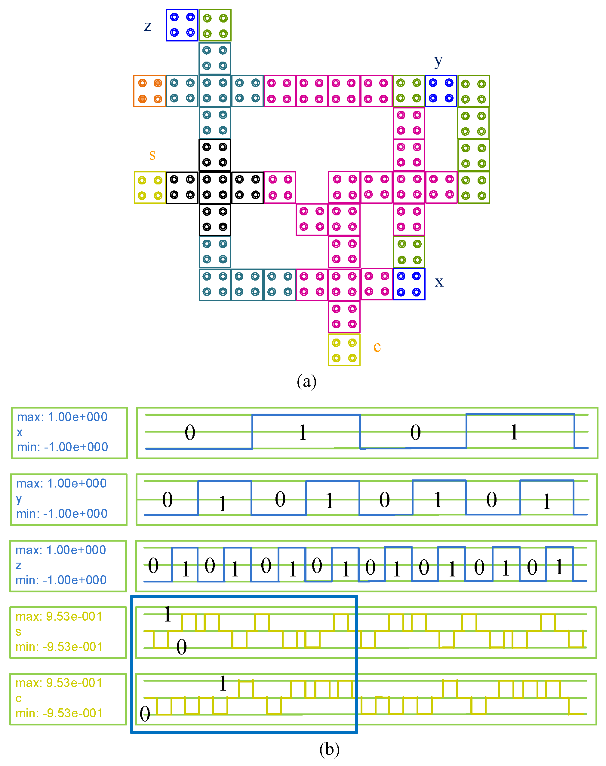
To achieve exceptional speed and efficiency, the study has developed a novel CSA with a highly optimised layout. As depicted in Figure 5a, the circuit’s 424 constituent cell blocks are arranged to achieve an exceptionally small area of just 0.56 μm2. This focus on dense cell integration is instrumental in curtailing propagation latency, setting a new benchmark against standard adder designs. The consequential performance gains, demonstrating the efficacy of the approach, are comprehensively illustrated in Figure 5b.
To enhance cross-verification, the QCAFA and CSA are modelled using Verilog HDL (12.0). This textual hardware representation provides functional abstraction and allows the design to be tested with standard EDA tools. The pseudocodes for the hardware design file (design.sv) and verification file (testbench.sv) for the QCAFA and CSA are presented in Table 2.
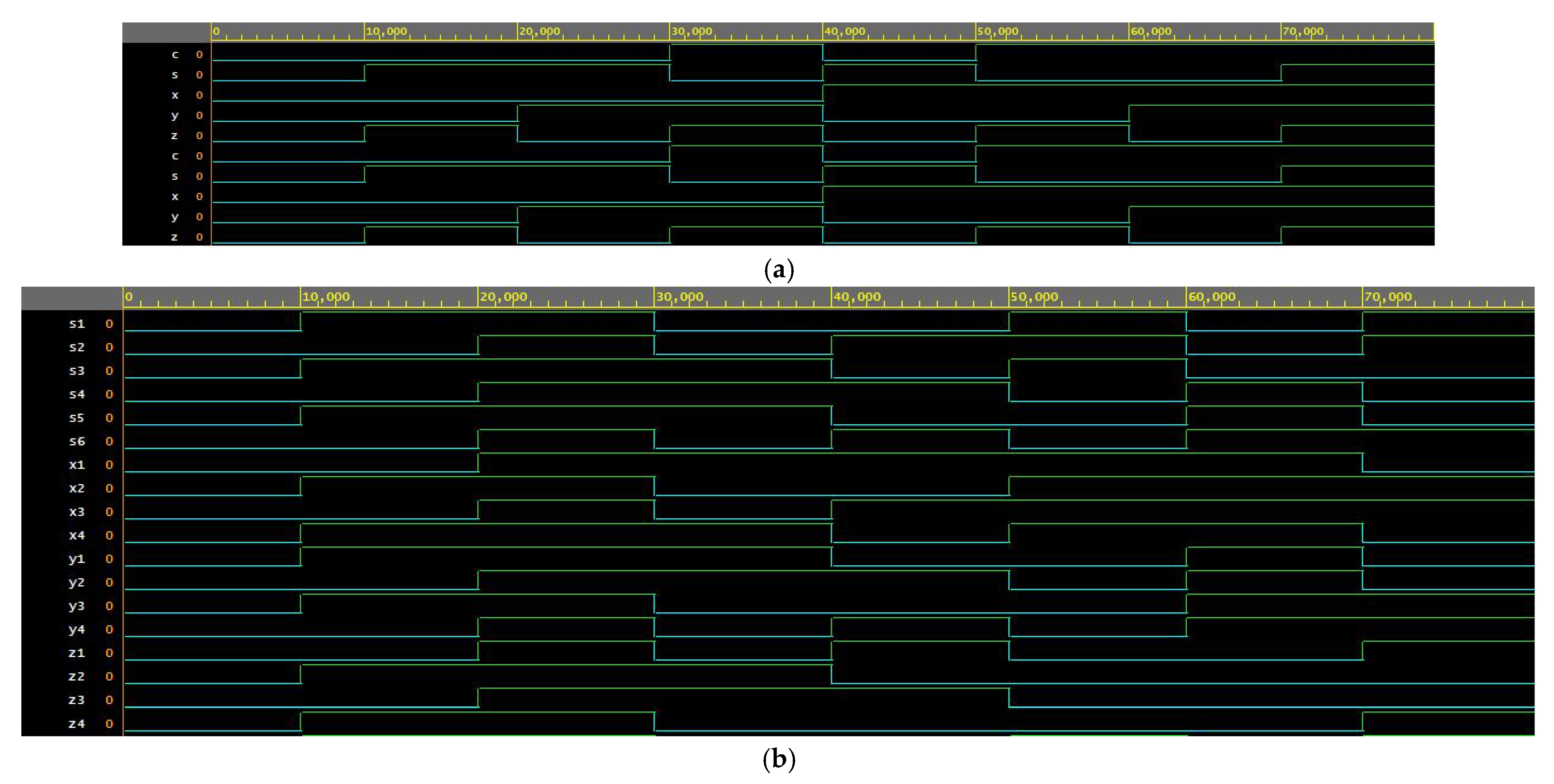
To validate the architecture at a hardware description level, a Verilog HDL model of the QCAFA and CSA is developed as presented in Figure 6a,b. The design is synthesised and simulated to confirm the correct functionality under exhaustive testbench scenarios.

4.1. Systematic Placement Methodology and Automation Strategy

To establish a reproducible and scalable design framework, this study adopts a systematic placement methodology that transforms the QCA circuit design process from manual refinement toward a rule-based, partially automated workflow. The methodology integrates logical abstraction, geometric regularity, and hierarchical synthesis to ensure that layout construction follows deterministic principles rather than empirical adjustments within QCADesigner.
The process begins with majority-logic decomposition, where Boolean expressions for each subcircuit are optimised into equivalent networks of three- and five-input majority gates and inverters. This representation enables the mapping of logic primitives onto pre-defined spatial templates, each characterised by standardised inter-cell distances and clocking zone assignments. These templates serve as reusable layout macros, ensuring consistent signal propagation and clock synchronisation across the design hierarchy.
Next, a structured placement protocol arranges the majority and inverter cells according to fixed geometric constraints, typically 90° and 45° orientations, while maintaining uniform separation between adjacent clock zones. Input, intermediate, and output cells are aligned along distinct spatial tracks to minimise signal interference and eliminate unnecessary wire crossings. Where intersections are unavoidable, the layout algorithm prioritises coplanar crossovers using controlled clock-phase offsets to preserve signal integrity. This procedure significantly reduces spatial redundancy and enhances manufacturability compared with random or visually guided placement.
To streamline layout generation, the proposed workflow incorporates a semi-automated placement strategy driven by parametric scripting. The QCA cells are positioned through coordinate-based scripts that define each cell’s logical role, clock zone, and connectivity. These scripts can be adapted or extended to generate alternative adder topologies with minimal manual intervention, thus providing a flexible automation framework. Once the initial layout is instantiated, QCADesigner serves as a verification platform rather than a design interface-confirming logical correctness, polarity propagation, and clock-phase synchronisation.
The final stage integrates HDL-level modelling and simulation to validate functional equivalence across abstraction layers. The Verilog HDL representation not only facilitates behavioural verification using standard EDA tools but also establishes a pathway toward future design automation through rule-based synthesis frameworks and optimisation scripts.
In essence, the proposed systematic methodology combines logic-driven placement, geometric regularity, and script-based automation to achieve reproducible, scalable, and technology-independent QCA circuit design. This structured approach ensures that the methodology remains generalisable to a wide range of arithmetic architectures, including ripple-carry, carry-lookahead, and reversible adders, thereby extending its applicability beyond the specific circuits demonstrated in this work.

4.2. Limitations of QCADesigner and Assumptions in Simulation

It is important to recognise that the simulations presented in this work were carried out using QCADesigner, which is not a physics-aware tool. Instead, QCADesigner operates under the assumption of neutral QCA cells, representing the most idealised conditions for circuit evaluation. This framework enables researchers to investigate the logical correctness, functionality, and scalability of QCA-based architecture, but it does not account for detailed physical effects such as quantum tunnelling dynamics and fabrication-related imperfections.
Accordingly, the results reported in this study should be interpreted as idealised functional outcomes, serving as a proof-of-concept demonstration of the nanoscale CSA design. While QCADesigner provides valuable insight into logic-level performance and circuit feasibility, further investigation using physics-based models and simulation platforms is essential to evaluate the robustness of the design under realistic operating conditions.
It should be noted that the QCADesigner simulation tool employed in this study does not inherently capture subtle timing discrepancies. Consequently, while the proposed design demonstrates correct logical functionality under simulation, the physical realisation of unbalanced voters could introduce synchronisation challenges. As highlighted in the recent literature [43,44], unbalanced structures raise concerns regarding robustness. By acknowledging this limitation, this research emphasises that the present work is primarily a proof-of-concept demonstration of the QCAFA and CSA architecture at logical and functional levels.
Furthermore, it should be clarified that the area values expressed in µm2 in this study, as in nearly all QCA literature, are derived directly from the default physical parameters embedded in QCADesigner rather than from any specific micrometric fabrication process. The simulation tool assumes a standard quantum cell dimension of 18 nm × 18 nm with 5 nm inter-dot spacing and a 2 nm dot diameter, which provides a consistent basis for reporting relative layout size across studies. Accordingly, the reported µm2 values are normalised, technology-independent indicators intended for comparative benchmarking with previously published QCA designs (e.g., [23,24,25,26,27,28,29,30,31,32,33,34,35,36,37,38,39,40,41,42,43,44,45,46]) rather than as physically realised silicon areas. Examples of similar conventions include Joy et al. [24] (0.078 µm2), Hasani and Navimipour [23] (0.37 µm2), and Erniyazov and Jeon [29] (0.66 µm2). To ensure clarity, the present manuscript also reports cell count and cell space alongside the µm2 area, providing a balanced, technology-neutral representation of design compactness.

4.3. Implementation Challenges and Strategic Solutions

While the compelling potential of QCA lies in its ultra-low power consumption and nanoscale integration capabilities, the practical realisation of a CSA within this paradigm is fraught with significant implementation hurdles. A primary challenge stems from the fundamental QCA reliance on cell-to-cell interaction, which supplants conventional physical wiring. In complex CSA architecture, this necessitates numerous wire crossings, which in turn precipitate signal interference, increase the physical footprint, and compromise overall circuit reliability. To mitigate these adverse effects, the proposed design incorporates coplanar crossovers, a sophisticated strategy for resolving signal path intersections without degrading performance.
Furthermore, the challenge of scalability becomes increasingly pronounced as the number of input bits expands. This escalation in complexity directly translates to a proliferation of QCA cells, a larger silicon area, and the heightened risk of signal degradation. To overcome this obstacle, this study advocates for a modular design philosophy, wherein smaller, reusable QCA building blocks are systematically integrated to form larger, more complex systems. This approach is complemented by hierarchical modelling and simulation-based optimisation, which streamlines the development of lifecycles and ensures design integrity at every stage of scaling.
An additional critical consideration lies in the domain of design, automation and analysis. While foundational tools such as QCADesigner provide essential support for circuit layout, they noticeably lack the capacity for accurate energy estimation, a vital metric for evaluating the ultra-low power promise of QCA. To address this analytical gap, the methodology leverages the QCADesigner-E tool, enabling a comprehensive energy profiling of the proposed architecture. Ultimately, through careful design analysis, the implementation of optimised clocking schemes, and detailed energy profiling, the study has successfully architected a CSA that is not only highly efficient but also robust and secure.

4.4. Potential Real-World Applications and Technological Impact

The design and analysis of CSA using QCA presents a compelling frontier for the next generation of energy-efficient, high-performance digital circuitry. A primary application domain lies in the development of highly optimised ALUs for ubiquitous computing platforms such as mobile electronics, embedded systems, and the burgeoning Internet of Things (IoT) ecosystem. In these contexts, where severe power budgets are paramount and computational throughput cannot be compromised, QCA-based CSAs offer a transformative pathway to achieving ultra-low power dissipation. The implications, however, extend far beyond these energy-constrained domains. The inherent speed and efficiency of QCA architecture position these adders as critical components in the demanding landscape of high-performance computing. They are exceptionally well-suited for computationally intensive fields, including cryptographic analysis, DSP, and real-time image rendering, where latency and power efficiency are decisive factors for system-level performance.
Looking toward the horizon of computational paradigms, QCA-based CSAs are composed of making pivotal contributions to the avant-garde fields of quantum and reversible computing. By facilitating the realisation of remarkably compact and energy-efficient arithmetic architectures, this technology addresses a fundamental challenge in constructing viable quantum-classical interfaces. This capability is of paramount importance, as conventional CMOS-based logic gates face fundamental physical limitations and are unsuitable for direct integration with future quantum computing systems, thereby establishing QCA as a vital enabling technology for the quantum era.

5. Comparative Analysis and Performance Evaluation

This section presents a rigorous evaluation of the novel QCAFA and CSA, benchmarked against contemporary state-of-the-art designs. Through extensive simulations, the study quantifies the impact of critical QCA parameters on overall circuit performance. The designed QCAFA, accurately engineered for ultra-low-power operation, exhibits a marked improvement in efficiency within the QCA paradigm. This performance gain is largely attributed to an innovative cell reduction strategy that strategically leverages rotation-based inverter logic, thereby minimising the total cell counts and structural footprint of the design. In nanoscale QCA circuits, minimising cell count, and resource cost enhances area efficiency and reduces latency; however, this reduction may also limit redundancy within the layout, potentially influencing the circuit’s tolerance to defects or thermal fluctuations. The proposed design seeks to balance this trade-off by maintaining compact architecture while still ensuring functional correctness under standard operating conditions. Although the present study primarily emphasises improvements in computational efficiency and implementation cost, the author recognises that future work should extend the evaluation toward robustness metrics, particularly under the influence of cell misalignment, fabrication defects, and thermal noise. The proposed QCAFA establishes a new performance benchmark, decisively outperforming contemporary designs [16,24,25,26,27,28,29,30,31,32,33,34,35,36,37] across a comprehensive set of metrics. The rigorous comparative analysis presented in Table 3 and Table 4 validates this claim, highlighting the QCAFA’s distinct advantages in critical areas such as cell block optimisation, area efficiency, area utilisation, resource economy, and operational latency.
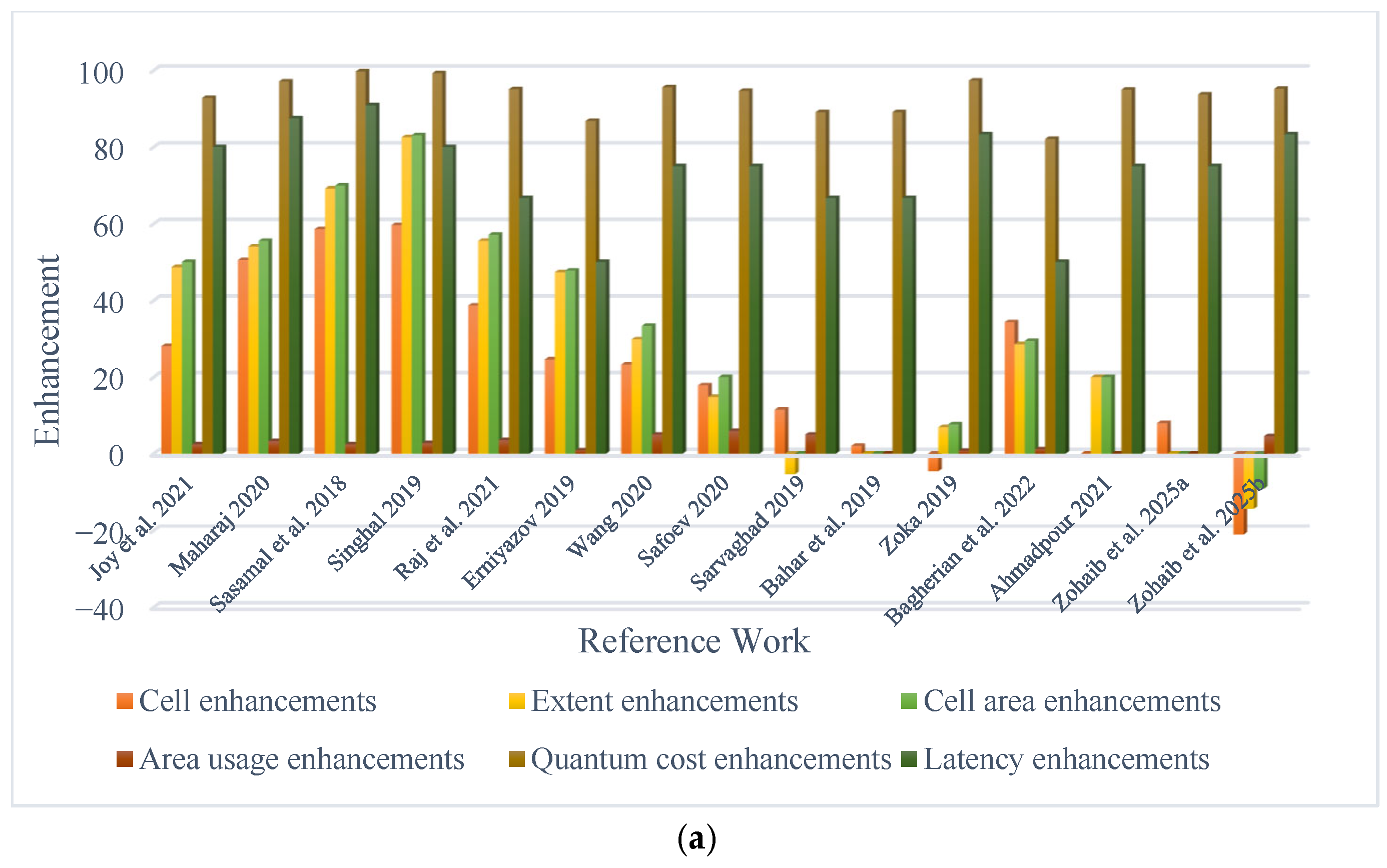
A comprehensive performance evaluation confirms that the proposed QCAFA architecture delivers substantial enhancements over existing designs. Against [24], it achieves improvements ranging from 28.13% (cell) to 92.86% (cost), including a significant 80% reduction in latency. When compared with [35], the QCAFA again shows superior performance, with enhancements up to 34.29% (cell) and 82.14% (resource cost). It also outperforms [37] with a 93.75% decrease in cost and a 75% decrease in latency. The evaluation also notes specific design trade-offs. The proposed QCAFA concedes a 5.26% area advantage to [32] and a 4.55% cell count advantage to [34]. It also shows reductions of 21.05%, 14.29%, and 9.09% in cell, space, and cell space metrics, respectively, when compared to [16]. Despite these specific metrics, the QCAFA architecture exhibits superior progress in all other factors, most notably in resource cost and latency, underscoring its overall efficacy. Table 4 provides a precise organisation of these comparative improvements.
Furthermore, the proposed CSA architecture demonstrates exceptional performance, as detailed in Table 5 and Table 6. It outperforms recent designs [23,29,38,40,45,46] across all metrics, a result attributed to its space-efficient adder, which enhances processing speed while minimising area. The CSA’s excellence in cost and delay metrics contributes to a substantial overall reduction in the total cost for both the QCAFA and CSA implementations when compared to existing models.
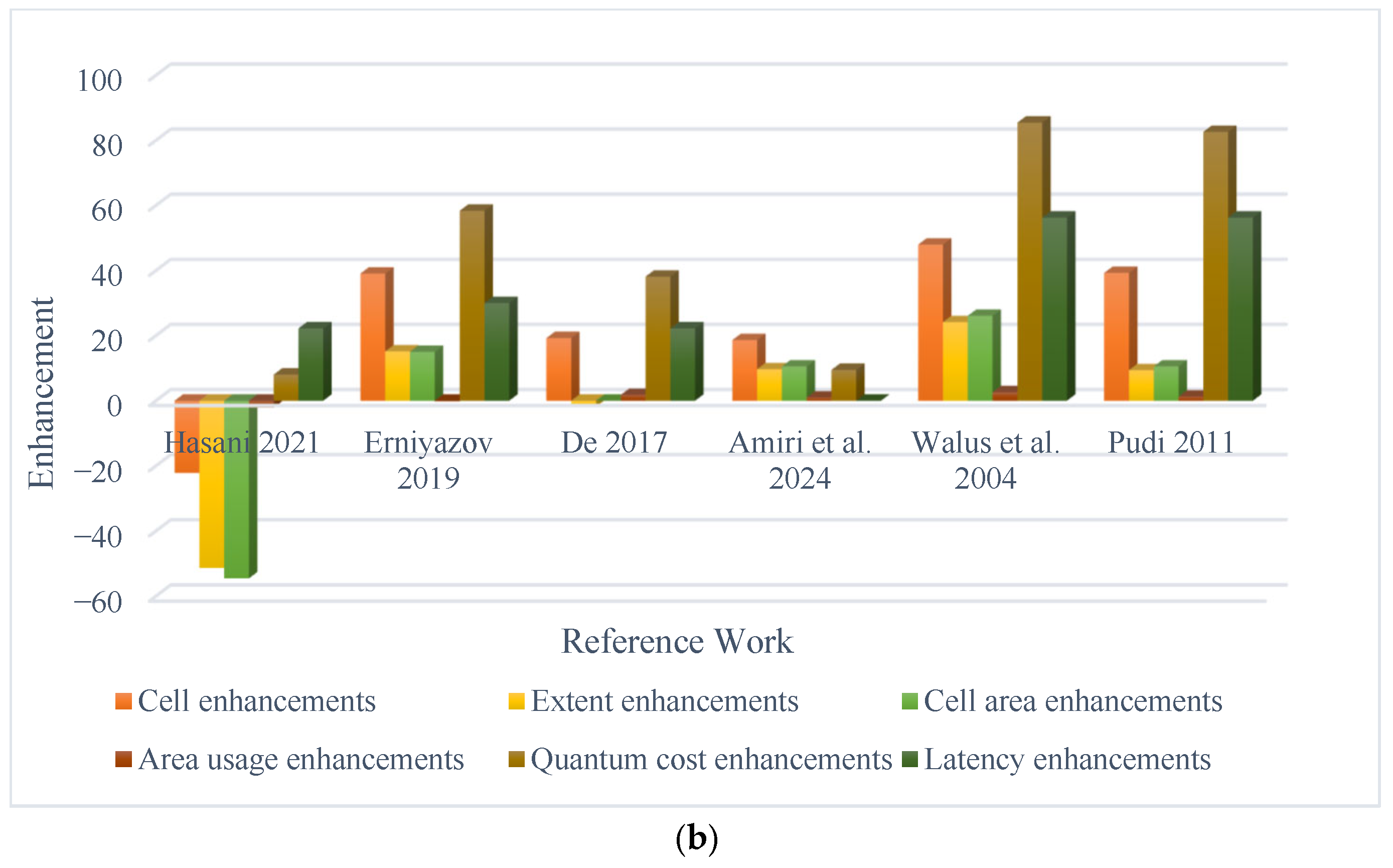
The proposed CSA demonstrates significant advancements over preceding layouts. In a benchmark analysis against the designs by De and Das [38], the proposed CSA achieves substantial improvements of 19.24% in cell count, 1.78% in area utilisation, 38.13% in cost, and 22.22% in latency. Furthermore, when juxtaposed with another contemporary layout, the proposed circuit registers performance gains of 47.98% in cell count, 24.12% in covered extent, 26.09% in cell extent, 2.60% in area utilisation, and a remarkable 85.44% in both cost and latency. It is crucial to note that the design in [23] exhibits a lower cell count, reduced area, and diminished cost. While the CSA shows a corresponding reduction of 22.19% in cell count, 51.35% in covered extent, 54.55% in cell extent, and 2.12% in area utilisation compared to this benchmark, it compensates with superior performance in the critical metrics of cost and latency, delivering enhancements of 8.02% and 22.22%, respectively. A pivotal distinction lies in the architectural approach: whereas the design in [23] employs a multilayer strategy, the proposed CSA leverages a streamlined single-layer methodology, potentially simplifying fabrication. In other comparative analyses, the designed CSA shows a marginal reduction of 1.82% in covered extent compared to [38] and 0.20% in area utilisation versus [29]. However, it consistently outperforms these alternatives in other vital considerations, including cell count, quantum cost, and latency. The comprehensive performance improvements for the CSA are meticulously summarised in Table 6, while Figure 7a,b provides a visual corroboration of the enhancements achieved by the outlined QCAFA and CSA.
Beyond these architectural and performance metrics, energy dissipation is a pivotal factor in evaluating the efficacy of QCA circuits. In contrast to conventional CMOS technology, where power loss is primarily due to resistive elements, energy loss in QCA circuits predominantly stems from the tunnelling and polarisation switching of cells [19]. Minimising this dissipation is therefore paramount for enhancing power efficiency, ensuring operational stability, and guaranteeing long-term circuit reliability [21]. A thorough analysis of energy dissipation is indispensable for designers aiming to optimise circuit performance, making it a cornerstone of QCA technology development. To quantify this crucial aspect, the study employed the QCADesigner-E simulation tool [50] for the evaluation. The resulting energy utilisation profiles for the proposed layouts are presented in Table 7.
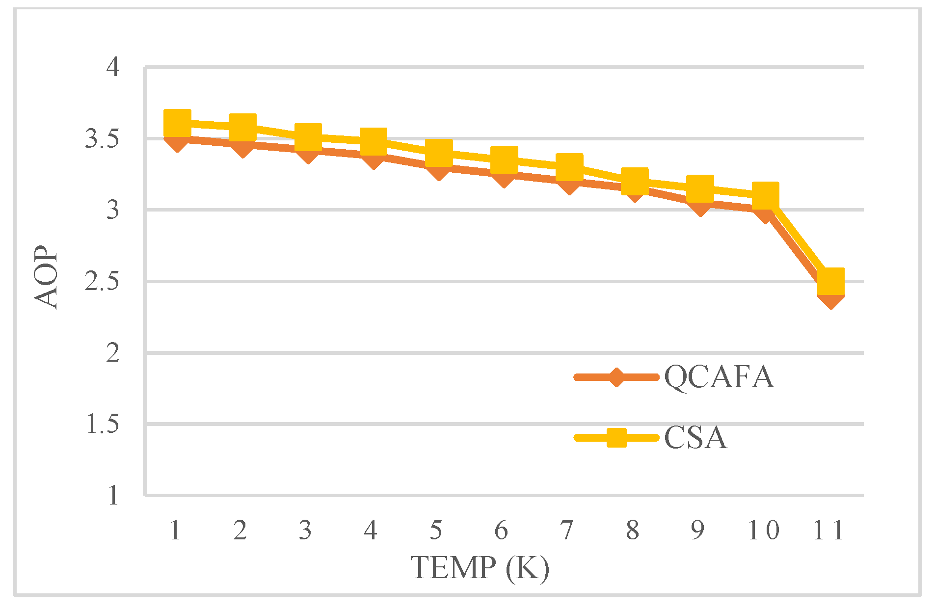
The thermal resilience of the proposed circuits was thoroughly investigated by scrutinising the dependence of output cell polarisation on temperature variations. Employing the QCADesigner simulation platform, the study quantified this effect through the Average Output Polarisation (AOP). This critical performance metric, defined as half the peak-to-peak polarisation swing, provides a direct measure of the output signal’s integrity and stability under thermal stress. AOP in QCA is the mean polarisation strength of the output cells, which is used to measure the circuit’s correctness, stability, and robustness against thermal effects [51]. This parameter provides a quantitative measure of the stability and reliability of output states under varying thermal conditions. The reported value of approximately 3.5 at lower temperatures arises from the pronounced separation between the maximum and minimum polarisation states when thermal noise is minimal. In such a regime, QCA cells retain strong polarisation, leading to a larger AOP. As the temperature increases, thermal fluctuations reduce this separation, which in turn decreases the AOP. Figure 8 provides a compelling validation of thermal resilience for the designed QCAFA and CSA designs. A critical analysis of the AOP values reveals that performance remains exceptionally stable, with only marginal deviations observed among the output cell blocks throughout the entire 1–10 K temperature range. This observation serves as a testament to the architecture’s high-fidelity operation and confirms its capacity to maintain reliable functionality under fluctuating cryogenic conditions.
In reporting the energy dissipation and operating temperature of the proposed QCA circuits, it is important to emphasise that these values are inherently implementation-dependent. The numerical results presented in this work were obtained using the QCADesigner and QCADesigner-E simulation framework with established tunnelling energy and kink energy parameters. These settings represent standard assumptions widely adopted in QCA research to ensure consistency and comparability across studies. Consequently, the reported figures should not be interpreted as absolute physical limits but rather as representative values under a well-defined simulation environment. By explicitly stating the modelling conditions, this research aims to provide clarity and reproducibility, enabling a fair and meaningful comparison of the presented designs with other QCA-based implementations in the literature.

6. Conclusions

QCA represents a transformative paradigm for the construction of digital systems at the nanoscale, promising to transcend the fundamental limits of conventional CMOS technology. However, the practical realisation of QCA-based arithmetic circuits has been persistently impeded by critical design challenges, including prohibitive cell complexity, excessive quantum cost, and unwieldy layout overhead. This research directly confronts these bottlenecks by introducing a novel class of single-layer QCA architectures for the fundamental QCAFA and the more intricate CSA. The design methodology is predicated on two synergistic principles: optimised majority-logic mapping and strategic layout minimisation, which collectively enable unprecedented efficiency. The resultant QCAFA architecture marks a significant breakthrough in circuit compactness. It is realised with a mere 46 cells, occupying a minimal footprint of 0.04 μm2 while achieving an exceptionally low latency of 0.25 clock cycles. This performance constitutes a remarkable reduction in cell count of up to 34.3% when benchmarked against the most advanced contemporary designs. Demonstrating the robustness and scalability of the approach, this design philosophy was extended to a QCA-based CSA. The proposed CSA architecture requires 424 cells within a condensed area of 0.56 μm2 and operates with a latency of 1.75 clock cycles, yielding an 18.6% improvement in cell utilisation over the best previously reported counterpart. Beyond architectural innovation, this work establishes a comprehensive verification framework by seamlessly integrating physical QCA layouts with HDL models. This dual-level verification methodology significantly enhances the fidelity of both physical and behavioural analyses for nanoscale circuits. The architecture presented herein is inherently modular and scalable, providing the foundational building blocks for constructing n-bit QCA-based CSAs. Furthermore, the core principles articulated in this work offer a versatile blueprint for the development of a wider array of essential arithmetic components, such as full subtractors and ripple carry adders, thereby plotting a course toward the design of more sophisticated and efficient nanoscale computational systems.

Funding

This research received no external funding.

Data Availability Statement

No new data were created or analysed in this study. Data sharing is not applicable to this article.

Acknowledgments

The author is deeply thankful to the anonymous reviewers for their valuable feedback and thoughtful suggestions.

Conflicts of Interest

The author declare no conflict of interest.

References

  1. Najmaei, S.; Glasmann, A.L.; Schroeder, M.A.; Sarney, W.L.; Chin, M.L.; Potrepka, D.M. Advancements in materials, devices, and integration schemes for a new generation of neuromorphic computers. Mater. Today 2022, 59, 80–106. [Google Scholar] [CrossRef]
  2. Radamson, H.H.; Zhu, H.; Wu, Z.; He, X.; Lin, H.; Liu, J.; Xiang, J.; Kong, Z.; Xiong, W.; Li, J.; et al. State of the art and future perspectives in advanced CMOS technology. Nanomaterials 2020, 10, 1555. [Google Scholar] [CrossRef]
  3. Lent, C.S.; Isaksen, B.; Lieberman, M. Molecular quantum-dot cellular automata. J. Am. Chem. Soc. 2003, 125, 1056–1063. [Google Scholar] [CrossRef] [PubMed]
  4. Walus, K.; Jullien, G.A.; Dimitrov, V.S. Computer arithmetic structures for quantum cellular automata. In Proceedings of the Thrity-Seventh Asilomar Conference on Signals, Systems & Computers, Pacific Grove, CA, USA, 9–12 November 2003; pp. 1435–1439. [Google Scholar]
  5. Jain, V.; Sharma, D.K.; Gaur, H.M.; Singh, A.K.; Wen, X. Comprehensive and comparative analysis of QCA-based circuit designs for next-generation computation. ACM Comput. Surv. 2023, 56, 1–36. [Google Scholar] [CrossRef]
  6. Ahmadpour, S.S.; Noorallahzadeh, M.; Al-Khafaji, H.M.R.; Darbandi, M.; Navimipour, N.J.; Javadi, B.; Ain, N.U.; Hosseinzadeh, M.; Yalcin, S. A new energy-efficient design for quantum-based multiplier for nano-scale devices in internet of things. Comput. Electr. Eng. 2024, 117, 109263. [Google Scholar] [CrossRef]
  7. Hofmann, S.; Walter, M.; Wille, R. Efficient and Scalable Post-Layout Optimization for Field-coupled Nanotechnologies. IEEE Trans. Comput. Aided Des. Integr. Circuits Syst. 2025, 44, 3790–3803. [Google Scholar] [CrossRef]
  8. Abdullah-Al-Shafi, M.; Bahar, A.N. An Architecture of 2-Dimensional 4-Dot 2-Electron QCA Full-adder and Subtractor with Energy Dissipation Study. Act. Passiv. Electron. Compon. 2018, 2018, 5062960. [Google Scholar] [CrossRef]
  9. Abdullah-Al-Shafi, M. Integration of nano routers into cryptographic circuits for scalable QCA architectures. Discov. Quantum Sci. 2025, 1, 2. [Google Scholar] [CrossRef]
  10. Gladshtein, M. Quantum-dot cellular automata serial decimal digit multiplier. J. Comput. Electron. 2025, 24, 54. [Google Scholar] [CrossRef]
  11. Vahabi, M.; Rahimi, E.; Bahar, A.N.; Wahid, K.A. Design of an energy efficient approximate BinDCT module in quantum cellular automata. Sci. Rep. 2025, 15, 19744. [Google Scholar] [CrossRef]
  12. Abdullah-Al-Shafi, M. Innovative reliable nanoscale QCA circuits for advanced morphological image processing. AIP Adv. 2025, 15, 045303. [Google Scholar] [CrossRef]
  13. Ahmadpour, S.S.; Jafari Navimipour, N.; Mosleh, M.; Noorallahzadeh, M.; Kassa, S.; Ahmed, S. A new fault-tolerance majority voter circuit for quantum-based nano-scale digital systems. J. Comput. Electron. 2025, 24, 149. [Google Scholar] [CrossRef]
  14. Seyedi, S.; Abdoli, H. A fault tolerant CSA in QCA technology for IoT devices. Sci. Rep. 2025, 15, 3396. [Google Scholar] [CrossRef] [PubMed]
  15. Abdullah-Al-Shafi, M.; Islam, M.S.; Bahar, A.N. 5-Input majority gate based optimized full-adder circuit in nanoscale coplanar quantum-dot cellular automata. Int. Nano Lett. 2020, 10, 177–195. [Google Scholar] [CrossRef]
  16. Zohaib, M.; Navimipour, N.J.; Aydemir, M.T.; Ahmadpour, S.S. A New Nano-Design of High-Speed Arithmetic and Logic Unit for Signal Processing Devices Based on Quantum-dot Technology. Nano Commun. Netw. 2025, 44, 100574. [Google Scholar] [CrossRef]
  17. Abdullah-Al-Shafi, M. RAM, DEMUX and ALU in nanoscale: A quantum-dot cellular automata-based architecture. Discov. Electron. 2025, 2, 26. [Google Scholar] [CrossRef]
  18. Marjeghal, M.A.; Sabbaghi-Nadooshan, R.; Ashrafian, A. A novel fault-tolerant T flip-flop in ternary QCA. Analog. Integr. Circuits Signal Process. 2025, 124, 56. [Google Scholar] [CrossRef]
  19. Vahabi, M.; Rahimi, E.; Lyakhov, P.; Otsuki, A. A novel QCA circuit-switched network with power dissipation analysis for nano communication applications. Nano Commun. Netw. 2023, 35, 100438. [Google Scholar] [CrossRef]
  20. Khan, A.; Shaw, R.K.; Bahar, A.N. A neural cantonese speech converter using QCA for nanocomputing. Comput. Electr. Eng. 2025, 126, 110536. [Google Scholar] [CrossRef]
  21. Seyedi, S.; Abdoli, H. Efficient design and implementation of approximate FA, FS, and FA/S circuits for nanocomputing in QCA. PLoS ONE 2024, 19, e0310050. [Google Scholar] [CrossRef]
  22. Ahmadpour, S.S.; Navimipour, N.J.; Ain, N.U.; Kerestecioglu, F.; Yalcin, S.; Avval, D.B.; Hosseinzadeh, M. Design and implementation of a nano-scale high-speed multiplier for signal processing applications. Nano Commun. Netw. 2024, 41, 100523. [Google Scholar] [CrossRef]
  23. Hasani, B.; Navimipour, N.J. A new design of a carry-save adder based on quantum-dot cellular automata. Iran. J. Sci. Technol. Trans. Electr. Eng. 2021, 45, 993–999. [Google Scholar] [CrossRef]
  24. Joy, U.B.; Chakraborty, S.; Tasnim, S.; Hossain, M.S.; Siddique, A.H.; Hasan, M. Design of an Area Efficient Quantum Dot Cellular Automata Based Full-Adder Cell Having Low Latency. In Proceedings of the 2nd International Conference on Robotics, Electrical and Signal Processing Techniques (ICREST), Dhaka, Bangladesh, 5–7 January 2021; pp. 689–693. [Google Scholar]
  25. Maharaj, J.; Muthurathinam, S. Effective RCA design using quantum dot cellular automata. Microprocess. Microsyst. 2020, 73, 102964. [Google Scholar] [CrossRef]
  26. Sasamal, T.N.; Singh, A.K.; Mohan, A. An efficient design of quantum-dot cellular automata based 5-input majority gate with power analysis. Microprocess. Microsyst. 2018, 59, 103–117. [Google Scholar] [CrossRef]
  27. Singhal, R.; Perkowski, M. Comparative Analysis of Full-Adder Custom Design Circuit Using Two Regular Structures in Quantum-Dot Cellular Automata (QCA). In Proceedings of the 49th International Symposium on Multiple-Valued Logic (ISMVL), Fredericton, NB, Canada, 21–23 May 2019; pp. 194–199. [Google Scholar]
  28. Raj, M.; Gopalakrishnan, L.; Ko, S.B. Design and analysis of novel QCA full-adder-subtractor. Int. J. Electron. Lett. 2021, 9, 287–300. [Google Scholar] [CrossRef]
  29. Erniyazov, S.; Jeon, J.C. Carry save adder and carry look ahead adder using inverter chain based coplanar QCA full-adder for low energy dissipation. Microelectron. Eng. 2019, 211, 37–43. [Google Scholar] [CrossRef]
  30. Wang, L.; Xie, G. A novel XOR/XNOR structure for modular design of QCA circuits. IEEE Trans. Circuits Syst. II Express Briefs 2020, 67, 3327–3331. [Google Scholar] [CrossRef]
  31. Safoev, N.; Jeon, J.C. Design of high-performance QCA incrementer/decrementer circuit based on adder/subtractor methodology. Microprocess. Microsyst. 2020, 72, 102927. [Google Scholar] [CrossRef]
  32. Sarvaghad-Moghaddam, M.; Orouji, A.A. New symmetric and planar designs of reversible full-adders/subtractors in quantum-dot cellular automata. Eur. Phys. J. D 2019, 73, 125. [Google Scholar] [CrossRef]
  33. Bahar, A.N.; Ahmad, F.; Wani, S.; Al-Nisa, S.; Bhat, G.M. New modified-majority voter-based efficient QCA digital logic design. Int. J. Electron. 2019, 106, 333–348. [Google Scholar] [CrossRef]
  34. Zoka, S.; Gholami, M. A novel efficient full-adder–subtractor in QCA nanotechnology. Int. Nano Lett. 2019, 9, 51–54. [Google Scholar] [CrossRef]
  35. Bagherian Khosroshahy, M.; Abdoli, A.; Rahmani, A.M. Design and power analysis of an ultra-high speed fault-tolerant full-adder cell in quantum-dot cellular automata. Int. J. Theor. Phys. 2022, 61, 23. [Google Scholar] [CrossRef]
  36. Ahmadpour, S.S.; Mosleh, M. Ultra-efficient adders and even parity generators in nano scale. Comput. Electr. Eng. 2021, 96, 107548. [Google Scholar] [CrossRef]
  37. Zohaib, M.; Navimipour, N.J.; Aydemir, M.T.; Ahmadpour, S.S. A nano-scale design of arithmetic and logic unit for energy-efficient signal processing devices based on a quantum-based technology. Clust. Comput. 2025, 28, 340. [Google Scholar] [CrossRef]
  38. De, D.; Das, J.C. Design of novel carry save adder using quantum dot-cellular automata. J. Comput. Sci. 2017, 22, 54–68. [Google Scholar] [CrossRef]
  39. Khan, A.; Bahar, A.N.; Arya, R. Efficient design of vedic square calculator using quantum dot cellular automata (QCA). IEEE Trans. Circuits Syst. II Express Briefs 2021, 69, 1587–1591. [Google Scholar] [CrossRef]
  40. Amiri, M.; Dousti, M.; Mohammadi, M. Design and implementation of carry-save adder using quantum-dot cellular automata. J. Supercomput. 2024, 80, 1554–1567. [Google Scholar] [CrossRef]
  41. Menon, A.; Miftah, S.; Kundu, S.; Kundu, S.; Srivastava, A.; Raha, A.; Sonnenschien, G.; Banerjee, S.; Mathaikutty, D.; Basu, K. Enhancing large language models for hardware verification: A novel systemverilog assertion dataset. ACM Trans. Des. Autom. Electron. Syst. 2025. [Google Scholar] [CrossRef]
  42. Cirstea, M.; Benkrid, K.; Dinu, A.; Ghiriti, R.; Petreus, D. Digital electronic system-on-chip design: Methodologies, tools, evolution, and trends. Micromachines 2024, 15, 247. [Google Scholar] [CrossRef]
  43. Ardesi, Y.; Beretta, G.; Vacca, M.; Piccinini, G.; Graziano, M. Impact of molecular electrostatics on field-coupled nanocomputing and quantum-dot cellular automata circuits. Electronics 2022, 11, 276. [Google Scholar] [CrossRef]
  44. Ardesi, Y.; Garlando, U.; Riente, F.; Beretta, G.; Piccinini, G.; Graziano, M. Taming molecular field-coupling for nanocomputing design. ACM J. Emerg. Technol. Comput. Syst. 2022, 19, 1–24. [Google Scholar] [CrossRef]
  45. Walus, K.; Dysart, T.J.; Jullien, G.A.; Budiman, R.A. QCADesigner: A rapid design and simulation tool for quantum-dot cellular automata. IEEE Trans. Nanotechnol. 2004, 3, 26–31. [Google Scholar] [CrossRef]
  46. Pudi, V.; Sridharan, K. Low complexity design of ripple carry and Brent–Kung adders in QCA. IEEE Trans. Nanotechnol. 2011, 11, 105–119. [Google Scholar] [CrossRef]
  47. Macrae, R.M. Mixed-valence realizations of quantum dot cellular automata. J. Phys. Chem. Solids 2023, 177, 111303. [Google Scholar] [CrossRef]
  48. Chen, H.; Zhao, L. Quantum-dot cellular automata as a potential technology for designing nano-scale computers: Exploring the state-of-the-art techniques and suggesting the opportunities for the future. Optik 2022, 265, 169431. [Google Scholar] [CrossRef]
  49. Majeed, A.; Alkaldy, E. A new approach to bypass wire crossing problem in QCA nano technology. Circuit World 2023, 49, 145–152. [Google Scholar] [CrossRef]
  50. Safaiezadeh, B.; Mahdipour, E.; Haghparast, M.; Sayedsalehi, S.; Hosseinzadeh, M. Design and simulation of efficient combinational circuits based on a new XOR structure in QCA technology. Opt. Quantum Electron. 2021, 53, 684. [Google Scholar] [CrossRef]
  51. Jeon, J.C.; Seo, C. Design of Fixed Cell-Based PLG Using Quantum-Dot Cellular Automata for Efficiency and Reliability of Digital Systems. IEEE Access 2024, 12, 187868–187876. [Google Scholar] [CrossRef]
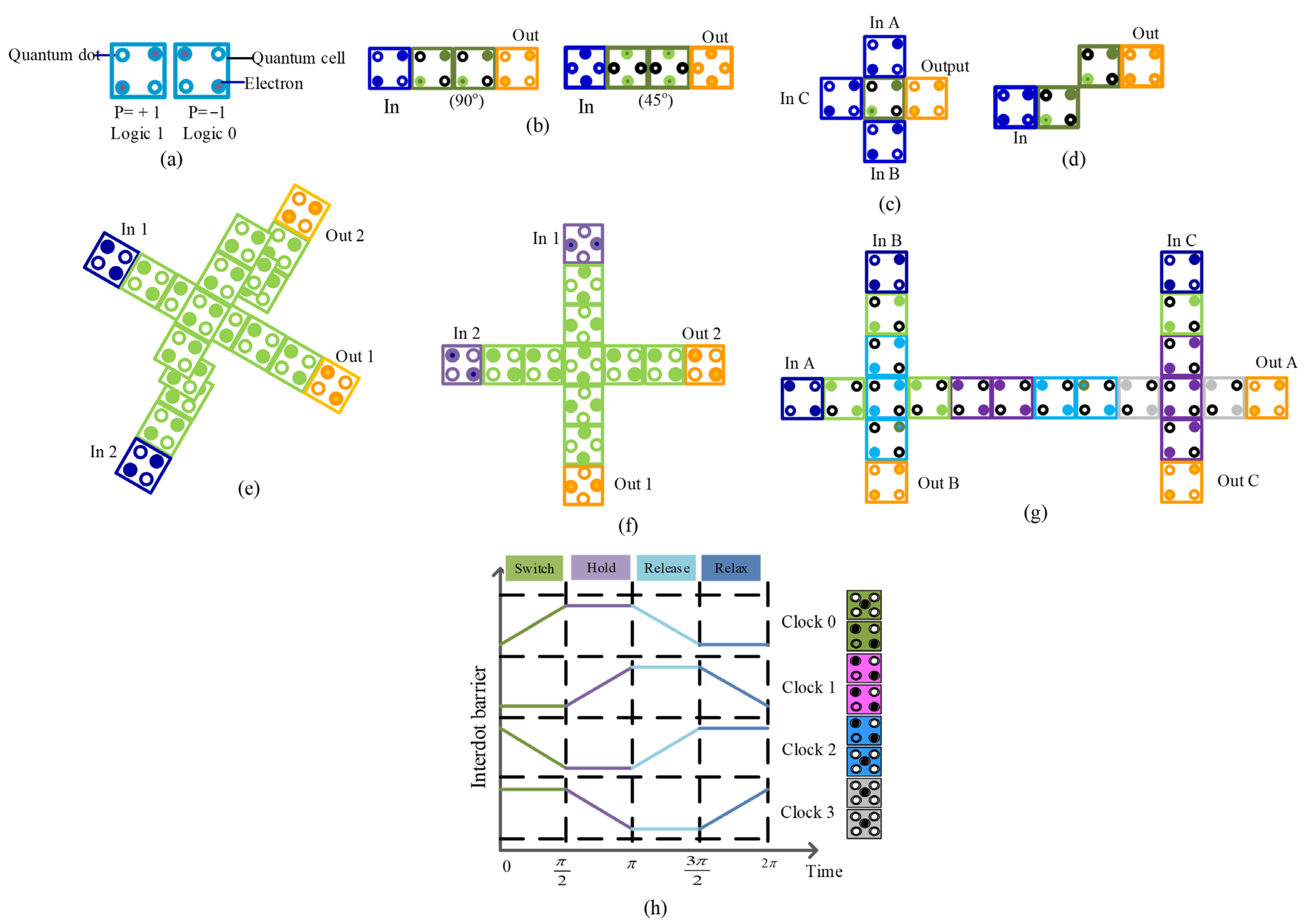
Figure 1. Key components and architectural elements of QCA: (a) fundamental cell structure, (b) wire configurations at 45° and 90°, (c) three-input majority gate, (d) inverter design, (e) planar signal crossover, (f) multi-layered crossover, (g) logic-level intersection, and (h) essential clocking scheme.
Chips 04 00043 g001
Figure 2. Cell faults in QCA: (a) missing, (b) dislocated, and (c) misaligned.
Chips 04 00043 g002
Figure 3. Designed QCA adder (a), outcome (b).
Chips 04 00043 g003
Figure 4. Proposed CSA structure.
Chips 04 00043 g004
Figure 5. Proposed QCA CSA (a), simulation outcome (b).
Chips 04 00043 g005
Figure 6. Verilog HDL design of QCAFA (a), CSA (b).
Chips 04 00043 g006
Figure 7. Overall improvement of QCAFA (a) [16,24,25,26,27,28,29,30,31,32,33,34,35,36,37], CSA (b) [23,29,38,40,45,46].
Chips 04 00043 g007aChips 04 00043 g007b
Figure 8. Output polarisation effect over the proposed QCAFA and CSA.
Chips 04 00043 g008
Table 1. Input-Output Mapping for the designed QCAFA.
InputOutput Response
xyzsc
00000
00110
01010
01101
10010
10101
11001
11111
Table 2. Pseudocodes for QCAFA and CSA.
QCAFACSA
design.sv:
function full_adder (x, y, z):
    s = x ^ y ^ z
    c = (x & y) | (y & z) | (x & z)
    return (s, c)
design.sv:
MODULE full_adder:
    INPUTS: x, y, z (1-bit each)
    OUTPUTS: s (sum), c (carry)
    s = x XOR y XOR z
    c = (x AND y) OR (y AND z) OR (x AND z)
END MODULE
// Carry-Save Adder Module (main design)
MODULE carry_save_adder:
     INPUTS:
           x1, y1, z1 (Triplet 1)
           x2, y2, z2 (Triplet 2)
           x3, y3, z3 (Triplet 3)
           x4, y4, z4 (Triplet 4)
     OUTPUTS:
           s1, s2, s3 (Sum outputs from triplets 1–3)
           s4, s5, s6 (Carry outputs from triplets 1–3)
     INTERNAL SIGNALS:
           fa1_s, fa1_c (Full adder 1 outputs)
           fa2_s, fa2_c (Full adder 2 outputs)
           fa3_s, fa3_c (Full adder 3 outputs)
     fa4_s, fa4_c (Full adder 4 outputs—unused)
     fa1 = full_adder (x1, y1, z1) → (fa1_s, fa1_c)
     fa2 = full_adder (x2, y2, z2) → (fa2_s, fa2_c)
     fa3 = full_adder (x3, y3, z3) → (fa3_s, fa3_c)
     fa4 = full_adder (x4, y4, z4) → (fa4_s, fa4_c)
     s1 = fa1_s
     s2 = fa2_s
     s3 = fa3_s
     s4 = fa1_c
     s5 = fa2_c
     s6 = fa3_c
END MODULE
testbench.sv
x, y, z = 0
s, c = 0
dut = full_adder (x, y, z, s, c)
dump_file (“full_adder.vcd”)
dump_vars (tb_full_adder)
for i in [0, 1, 2, 3, 4, 5, 6, 7]:
    {x, y, z} = i
    wait (10)
    log (time, x, y, z, s, c)
end_simulation ()
testbench.sv
MODULE tb_carry_save_adder:
     SIGNALS: x1, y1, z1, x2, y2, z2, x3, y3, z3, x4, y4, z4
     SIGNALS: s1, s2, s3, s4, s5, s6
     dut = carry_save_adder (x1, y1, z1, x2, y2, z2, x3, y3, z3, x4, y4, z4, s1, s2, s3, s4, s5, s6)
     INITIAL:
     SET (x1, y1, z1, x2, y2, z2, x3, y3, z3, x4, y4, z4) = 12′b000000000000
     WAIT 10 time units
     SET (x1, y1, z1, x2, y2, z2, x3, y3, z3, x4, y4, z4) = 12′b010101010101
     WAIT 10 time units
     SET (x1, y1, z1, x2, y2, z2, x3, y3, z3, x4, y4, z4) = 12′b111111111111
     WAIT 10 time units
     SET (x1, y1, z1, x2, y2, z2, x3, y3, z3, x4, y4, z4) = 12′b110011001100
     WAIT 10 time units
     SET (x1, y1, z1, x2, y2, z2, x3, y3, z3, x4, y4, z4) = 12′b101010101010
     WAIT 10 time units
     SET (x1, y1, z1, x2, y2, z2, x3, y3, z3, x4, y4, z4) = 12′b100100100100
     WAIT 10 time units
     SET (x1, y1, z1, x2, y2, z2, x3, y3, z3, x4, y4, z4) = 12′b110110110110
     WAIT 10 time units
     SET (x1, y1, z1, x2, y2, z2, x3, y3, z3, x4, y4, z4) = 12′b001100110011
     WAIT 10 time units
     CALL $finish ()
     INITIAL:
          CALL $dumpfile (“carry_save_adder.vcd”)
          CALL $dumpvars (0, tb_carry_save_adder)
     INITIAL:
          MONITOR (
            “Time = %0t: In1 = %b%b%b In2 = %b%b%b In3 = %b%b%b In4 = %b%b%b | Out = %b%b%b%b%b%b”,
            $time,
            x1, y1, z1, x2, y2, z2, x3, y3, z3, x4, y4, z4, s1, s2, s3, s4, s5, s6)
END MODULE
Table 3. Comparison of QCAFA circuits.
AddersCell IntricacySpace in (µm2)Cell Space
(µm2)
Area
Engagement (%)
Resource CostLatencyCell RatioRobustness/Fault Tolerance
In [24]640.0780.02430.770.0351.251.39Not discussed
In [25]930.0870.02731.030.08722.02Not discussed
In [26]1110.130.04030.770.98312.752.41Cell displacement and cell misalignment
In [27]1140.230.07130.870.3591.252.48Not discussed
In [28]750.090.02831.110.0510.751.63Missing
cell defects, misalignment defects, additional cell defects, and struck-at-faults
In [29]610.0760.02330.260.0190.51.33Not discussed
In [30]600.0570.01831.580.05711.30Not discussed
In [31]560.0470.01531.910.04711.22Not discussed
In [32]520.0380.01231.580.0230.751.13Cell displacement and cell misalignment
In [33]470.040.01230.000.0230.751.02Not discussed
In [34]440.0430.01330.230.0961.50.96Not discussed
In [35]700.0560.01730.360.0140.51.52Fault-tolerant
In [36]460.050.01530.000.0511.00Not discussed
In [37]500.040.01230.000.0411.08Not discussed
In [16]380.0350.01131.430.05251.50.826Not discussed
Proposed 460.040.01230.000.00250.251.00Not evaluated
Table 4. Enhancements assessment of QCAFA.
LayoutsCell (%)Space (%)Cell Space (%)Area Usage
(%)
Resource Cost
(%)
Latency
(%)
In [24]28.1348.7250.002.5092.8680.00
In [25]50.5454.0255.563.3297.1387.50
In [26]58.5669.2370.002.5099.7590.91
In [27]59.6582.6183.102.8299.3080.00
In [28]38.6755.5657.143.5795.1066.67
In [29]24.5947.3747.830.8686.8450.00
In [30]23.3329.8233.335.0095.6175.00
In [31]17.8614.8920.005.9994.6875.00
In [32]11.54−5.260.005.0089.1366.67
In [33]2.130.000.000.0089.1366.67
In [34]−4.556.987.690.7697.4083.33
In [35]34.2928.5729.411.1982.1450.00
In [36]0.0020.0020.000.0095.0075.00
In [37]8.000.000.000.0093.7575.00
In [16]−21.05−14.29−9.094.5595.2483.33
Table 5. Comparison of CSA circuits.
CSA Cell IntricacySpace in (µm2)Cell Space
(µm2)
Area
Employment (%)
Resource
Cost
LatencyCell
Ratio
In [23]3470.370.1129.731.872.250.82
In [29]6960.660.2030.304.132.501.64
In [38]5250.550.1730.912.782.251.24
In [40]5210.620.1930.651.901.751.23
In [45]8150.7380.2331.1711.8141.92
In [46]6980.6180.1930.749.8941.65
Proposed4240.560.1730.361.721.751
Table 6. Enhancements assessment of CSA.
QCA LayoutCell Block (%)Extent (%)Cell Area (%)Area Usage
(%)
Resource Cost
(%)
Latency (%)
In [23] −22.19−51.35−54.55−2.128.0222.22
In [29]39.0815.1515.00−0.2058.3530.00
In [38]19.24−1.820.001.7838.1322.22
In [40]18.629.6810.530.959.470.00
In [45]47.9824.1226.092.6085.4485.44
In [46]39.269.3910.531.2482.6156.25
Table 7. Power depletion by the presented circuits in eV.
QCA ArchitectureDepletion of Total EnergyDepletion of Average Energy
Proposed QCAFA1.34 eV1.18 eV
Proposed CSA3.80 eV3.60 eV
Disclaimer/Publisher’s Note: The statements, opinions and data contained in all publications are solely those of the individual author(s) and contributor(s) and not of MDPI and/or the editor(s). MDPI and/or the editor(s) disclaim responsibility for any injury to people or property resulting from any ideas, methods, instructions or products referred to in the content.