Abstract
Microwave-driven quantum logic gates in trapped-ion systems offer a scalable and laser-free alternative to optical control, with the potential for robust integration into surface-electrode trap architectures. In this work, we present a systematic design guideline for planar ion traps optimized for fast two-qubit microwave gates using chip-integrated conductors. We investigate two electrode configurations, one employing a single microwave line for driving transitions, and another with two symmetric lines for transitions. Through finite-element simulations, we analyze ion height, magnetic field gradients, heating effects, and gate durations under realistic cryogenic conditions. Our results show that both configurations can achieve two-qubit gate times in the order of 10 μs for and ions.
1. Introduction
Trapped ions remain one of the most promising platforms for the realization of universal quantum processors, offering long coherence times [1,2] and high-fidelity quantum gates necessary for fault-tolerant quantum computing [3,4]. Quantum logic operations have been successfully demonstrated using both single-qubit [5] and entangling two-qubit [6,7] gates with fidelities suitable for implementing error correction protocols. These qubits are typically based on electric-dipole-forbidden transitions, either of optical frequency, such as electric quadrupole transitions [8], or in microwave (MW) domain between hyperfine levels [9], allowing for a remarkably long coherence time on the order of several minutes or even more due to suppressed spontaneous emission [10]. While the optical qubits are operated with carefully tuned lasers, the microwave qubits are also usually controlled using optical Raman transitions to achieve individual addressing [11] and to couple internal states to motional modes [12]. However, this laser-based approach introduces challenges such as photon scattering [13,14] and the need for complex optical alignment when scaling up to larger systems.
Microwave-driven qubit operations offer an attractive alternative, particularly in terms of scalability, system stability, and cost-effectiveness [15,16]. However, implementing precise spatial addressing and strong spin-motion coupling with microwave fields in free space is challenging due to their long wavelengths. To overcome this, methods have been developed to enhance field gradients, either by applying strong magnetic field gradients [17,18,19] or by placing ions near microwave-carrying conductors, leveraging near-field effects [20,21]. This enables precise control over spin-motion coupling through trap-integrated microwave structures. Recent progress in integrating microwave circuitry directly into surface-electrode ion traps has opened new avenues towards realizing scalable quantum processors [16,22]. These microfabricated traps enable high-fidelity quantum gates comparable to those achieved with lasers [15], but with enhanced engineering control. Moreover, planar ion traps provide greater scalability when integrated into the quantum charge-coupled device (QCCD) architecture [23].
In particular, the transition within the hyperfine manifold can be utilized for microwave-driven quantum operations using chip-integrated conductors [15]. To drive this transition, a patterned conductor layout with shared AC current paths is employed. By displacing the ion perpendicular to the trap axis and applying an alternating current, a time-varying magnetic field is generated at the ion’s position, enabling coherent Rabi oscillations. When applied to a pair of ions, this configuration can induce spin-motion coupling, facilitating entangling gate operations. Additionally, the transition, driven by microwave fields aligned along the quantization axis, can also be employed for qubit manipulation [16,24]. The first experimental realization of a two-qubit gate driven solely by microwave fields was demonstrated in 2009 using a magnetically insensitive transition in a ion [21]. This implementation used a three-conductor layout to generate a microwave magnetic field gradient and achieved a two-qubit gate fidelity of 76% with a gate time of 400 μs. High-fidelity microwave-driven gates were later demonstrated in 2016. In one approach, a static magnetic field gradient was used to entangle ions with 98.5% fidelity and a 2700 μs gate time [25]. In another, a microwave field gradient enabled a 99.7% fidelity gate in , albeit with a longer gate time of 3250 μs [5]. A recent study on ions reported a faster two-qubit gate of 99.3% fidelity within 1000 μs [26]. Despite the high fidelity, these microwave-based gates remained significantly slower than optical Mølmer–Sørensen gates, such as those demonstrated with ions in [6]. A major improvement in gate speed was recently reported in [15], wherein a gate duration of 120 μs was achieved. However, this result relied on a magnetically sensitive qubit encoding, which inherently limits the achievable coherence time.
In this work, we numerically investigate planar ion trap configurations with different electrode layouts optimized for fast two-qubit microwave gates using magnetic field gradients, while maintaining qubit encoding on hyperfine splitting. Our goal is to find an optimal parameters to achieve fast gate operation, paving the way for scalable, laser-free quantum computation in trapped-ion systems. Specifically, we focus on two chip configurations with, respectively, a single MW line and two MW lines, and conduct numerical simulations of magnetic field distribution, temperature distribution, and estimate gate operation time. For both and ions, we demonstrate the possibility of achieving a fast two-qubit gate in the order of ten microseconds under realistic experimental conditions, demonstrating the validity of our proposed guideline of chip design.
2. Microwave Trap Designs
Microwave quantum gates require the ability to drive transitions between hyperfine states. These transitions can involve a change in the projection of the total atomic angular momentum, m, by 0 or . Accordingly, two types of transitions are possible: and transitions. The transitions preserve the magnetic quantum number () and are driven by linearly polarized electromagnetic fields aligned with the quantization axis. In contrast, transitions involve a change of and are induced by circularly polarized fields perpendicular to the quantization axis.
An external static magnetic field is applied to lift the degeneracy of the magnetic sublevels of the hyperfine manifold, a prerequisite for implementing microwave-based quantum logic. Typically, this DC magnetic field lies in the plane of the chip, with a significant projection along the x-axis, perpendicular to the ion chain and parallel to the trap surface. To implement a microwave-driven two-qubit gate, it is essential to generate a strong gradient of the oscillating magnetic field component along the x-direction, , while minimizing the DC component of the microwave field, , at the ion position. This oscillating magnetic field gradient couples the internal qubit states to the collective motional modes of the ion chain. The strength of this coupling, and hence the effective Rabi frequency, is directly proportional to the magnetic field gradient. Under these conditions, the duration of a microwave-driven two-qubit gate can be estimated as follows:
where is the mass of the ion, is the secular frequency of the trapping potential, and is the magnetic dipole matrix element associated with the transition. Therefore, in order to realize a fast two-qubit gate, it is crucial to generate a strong gradient of the oscillating magnetic field while simultaneously nullifying the static component of the microwave field at the ion position [20].
To enable the individual addressing of ions [27], it is necessary to displace specific ions along the x-axis, moving them into regions where the microwave magnetic field component is non-zero. In these regions, both single- and two-qubit gates can be performed. Such displacement can be achieved using auxiliary DC electrodes integrated into the surface trap design. Furthermore, the microwave magnetic field can be generated using pulsed currents, which provides temporal control, allowing the field to be turned on or off as required during gate operations.
We consider three schemes to generate the conditions required to implement microwave gates (see Figure 1). In all cases, the external static magnetic field is assumed to be aligned along the x-axis. For simplicity and practical feasibility, we only analyze configurations in which the same current flows through each conductor. Using identical currents avoids the need for precise calibration and stabilization of the current amplitude and phase, which would be necessary in more complex configurations with individually controlled conductors.
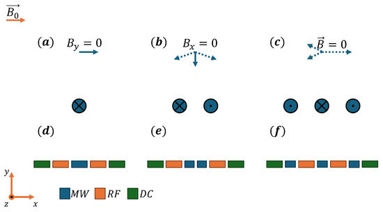
Figure 1.
Schemes used for passively nulling magnetic fields. The magnetic fields generated by each single MW wire are denoted by dotted lines, and the total field is denoted by solid lines. (a,b)—magnetic filed generated above single current and pair of oppositely directed currents respectively; (c)—magnetic field in the null point above the three current scheme; (d–f)—layout the single, two and three current scheme on surface trap respectively.
In the first scheme [15] (Figure 1a), a single current generates a microwave magnetic field parallel to the x-axis at a point above the wire, thus ensuring that . The gradient is non-zero, making this configuration suitable for two-qubit gate operations. However, to drive a transition, the polarization of the field gradient should be aligned with the DC magnetic field direction, which is not the case here. Instead, the resulting polarization is a superposition of and components, thus enabling the generation of transitions with . The second scheme [16] (Figure 1b) utilizes two currents of equal magnitude flowing in opposite directions, creating a field perpendicular to the trap plane at the center. In this configuration, the polarization of the microwave field gradient aligns with the DC magnetic field, enabling the induction of transitions. The third configuration [22] (Figure 1c) consists of three equidistantly placed wires carrying the same current, which nullifies the AC magnetic field at a specific point. At this point, the gradient of the field along the x–y axes is non-zero, allowing both and transitions. Simple calculations show that, in the ideal case, the position where the AC field is nulled is located at a distance equal to the spacing between the wires, above the central wire.
3. Materials and Methods
The ion height must be carefully chosen during the trap design process. An increased distance between the electrodes and the ion results in a higher numerical aperture, which facilitates more efficient ion cooling. Furthermore, the ion heating rate decreases rapidly with increased ion height, scaling as . As the distance from the dielectric increases, the electric field noise decreases, leading to lower-qubit gate errors. On the other hand, the depth of the potential well decreases with increasing ion height. Moreover, when introducing an MW line for near-field interactions, a smaller distance is preferable, as the impact of the magnetic field is enhanced. As a result, the ion height must be carefully selected to balance these competing factors.
Once the ion-to-electrode distance is fixed, the geometry of the DC and radio-frequency (RF) electrodes must be defined to maintain the desired height. We consider a standard five-rail scheme with DC-RF-DC-RF-DC electrodes. The defined geometry of the trap now allows for the placement of MW lines to drive current. We examine three possible electrode placement schemes, (a) one conductor, (b) two conductors, and (c) three conductors, all with equal current amplitude but flowing in different directions (see Figure 1 and Figure 2).
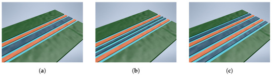
Figure 2.
View of electrode layout with different configurations. The colors on this figure corresponds to colors on Figure 1d–f. (a) Trap configuration with single MW line. (b) Trap configuration with two MW lines. (c) Trap configuration with three MW lines.
In design (a), the current flows through the central DC electrode, which is maintained at a potential close to zero. This configuration does not significantly perturb the pseudopotential distribution across the electrodes but generates a magnetic field predominantly along the x-axis (Figure 1d and Figure 2a). In design (b), the central DC electrode is split into two microwave conductors, separated by a gap equal to that between the RF and DC electrodes. This gap minimally distorts the trapping pseudopotential while allowing current to flow in opposite directions through the two MW lines, generating a magnetic field along the y-axis, as illustrated in Figure 1e and Figure 2b. The third design, design (c), has two additional microwave lines located between the RF and outer DC electrodes, as depicted in Figure 1f and Figure 2c. The central electrode is also used as an MW line, forming a three-conductor setup. This configuration allows for the generation of a magnetic field with a null point above the trap surface. Ideally, the zero-crossing of the magnetic field coincides with the minimum of the pseudopotential.
An additional critical consideration in planar trap design is the heating induced by the microwave current. While a higher magnetic field gradient is desirable for faster gate operations, the current is limited by the power dissipation that can be extracted from the chip and the maximum allowable temperature, which is particularly important in a cryogenic environment. Therefore, the electrode dimensions, thermal management capabilities, and maximum operating temperature collectively constrain the allowable current.
With the electrode geometry defined, the next step is to tune the RF voltage parameters—specifically, the amplitude and frequency—in order to achieve the desired stability parameter, secular frequency, and trap depth.
4. Numerical Results
For our numerical simulation, we consider a five-electrode design with the central DC of width , two symmetric RF electrodes on the side of width , and two outer DC electrodes with a size of 500 μm. The gap between electrodes is 10 μm. We define the grid with a 10 μm step for each value (18 × 18 values in total) and calculate the height of ions above the surface with the finite-element method (FEM, COMSOL Multiphysics 6.1). In Figure 3, we can see the dependence between and for for scheme (a). For other schemes, the dependence is similar since the only difference is the small gaps for the MW lines. Note that it is possible to achieve the same with different configurations of electrodes.
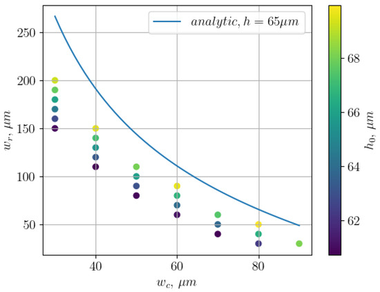
Figure 3.
The dependence between and for the scheme (a) with . The blue line is an analytical solution [28].
The height of ions can also be qualitatively estimated using an analytic model [28], as follows:
However, this approach (blue line in Figure 3) does not account for the gaps between electrodes and therefore introduces errors. Consequently, the field distribution and the ion height above the trap are usually computed numerically.
For the next stage, we choose values of and to give . For configurations (a) and (b), the choice of and defines the design uniquely and there are no free parameters. In design (c), we introduced the parameter , which corresponds to the width of the two outer MW lines. The aim of this configuration was to have the pseudopotential minima at the same point as the zero point of the AC magnetic field. However, we did not find any solution for (, , ) to fulfill this requirement. This happened for the following reason: As mentioned in Section 2, the height of ions above the trap surface is the same as the distance between MW currents for configuration (c). But here, the distance between currents defines the magnetic null, which is far beyond the target height of . Thus, in the following discussion we focus on configurations (a) and (b) only.
To determine the upper bound of the current, we conduct heating simulations using FEM (COMSOL Multiphysics). For designs (a) and (b), we calculate the maximum AC current, which is a major heat source. We choose the height of the silicon substrate as 500 μm, and the thickness of the gold electrodes as 500 nm. The temperature at the bottom of the substrate is set to 6 K. We calculate the maximum current that can be used while keeping the temperature below 10 K on the surface of the chip. In our simulation, a harmonic current with constant amplitude is applied to the MW electrodes, and the equilibrium of this system is calculated. The whole power from the MW line is pumped by the cooler at the bottom of the substrate. The pumped power is about 2 W per 1 mm of trap length, which is realistic and accessible in an experimental environment. Also, we consider different forms of current distribution across a single conductor and compare the results with a uniform distribution. The deviation is less than 1%; therefore, in further simulations we assume a uniform distribution of current density in the MW lines. Examples of temperature distribution are presented in Figure 4.
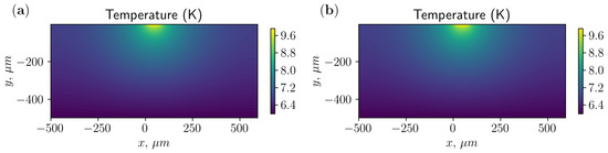
Figure 4.
The temperature distribution for configurations (a,b), with parameters = 80 μm and = 40 μm.
For the next step, we simulate an electromagnetic field and define the height of ions and the gradient of the microwave magnetic field. Examples of magnetic field distribution are presented in Figure 5, wherein the gradient of the microwave magnetic field is presented as a function of the height for both configuration (a) and configuration (b). For a silicon substrate with high resistivity and the geometric parameters considered here, the dielectric loss in silicon and capacitance coupling between electrodes have negligible effects on the field distribution around the ion position. Thus, we do not consider these effects, as in previous works [24,26]. Notice that while the gradient changes significantly with height for both schemes, the variation in (b) is much sharper than that in (a). For higher positions, the width of the MW wire ceases to play a role, since it looks like a single line with a negligible cross-section. However, the resistance of the MW wire decreases with increasing width and allows larger currents to flow. This leads to higher field gradients for wider MW wires. For short distances, the MW wire cannot be considered as a one-dimensional line. In that case, the field gradient becomes smaller for wider MW wires. This is because the current density is lower when spread over a wider surface. Since the field contribution from each wire segment decreases with distance and current density, the electrodes produce a weaker total field.
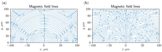
Figure 5.
The magnetic filed lines for configurations (a,b), with parameters = 80 μm, = 40 μm.
To gain a better understanding of the simulation result, we perform an analytic estimation of magnetic field gradient and show some typical data for different configurations in Figure 6. For scheme (a), we consider a single wire with current I and calculate the gradient above the wire as . This analytical model agrees well when simulating for a large distance, as the effect induced by the finite size and detailed geometry of the wire becomes negligible. At a small distance, the discrepancy becomes significant (see Figure 6a). For scheme (b), we place two wires with opposite currents separated by a distance L and calculate the gradient above the middle as . The agreement with the numerical simulation is also good at a large distance, as noted in Figure 6b. We further notice that the asymptotical dependence of the field gradient on the distance is different for the two configurations, with for scheme (a) and for (b).
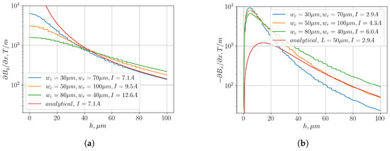
Figure 6.
Examples of MW magnetic field gradients for different and values with maximum current. (a) for the single-wire configuration; (b) for the configuration with two wires.
Furthermore, we stress that the duration of a two-qubit gate depends on the maximum temperature of the chip, since it determines the maximal current, which in turn sets the field gradient that governs the gate time. Therefore, achieving fast two-qubit gates requires the use of a cryogenic setup. Additionally, the substrate acts as an intermediate element between the heat source and the coldfinger of the cryostat, and the chip’s maximum temperature can be reduced by using a substrate with higher thermal conductivity.
Before concluding, we present in Table 1 the maximal currents, gradients of the magnetic fields, and two-qubit gate time for configurations (a) and (b). For each case, we calculate the magnetic field gradient at the ion position. Different schemes yield different gradients, since the current distribution on the surface is different. In configuration (a), with one wire, the induced transition is a transition, so only the linearly polarized part of the MW field projected on polarization is considered to obtain the field gradient and gate time. Here, the gate time is calculated both for a ion (: and : for hyperfine splitting of the ground state equals 1.25 GHz) in a trap with a secular frequency of 6 MHz, as well as for a ion (: and : for hyperfine splitting of the ground state equals 3.1 GHz) in a trap with a secular frequency of 3 MHz.

Table 1.
Calculated maximal currents, field gradients, and two-qubit gate times for different MW chip configurations.
Notice that in configuration (a), the ion height should be the same as that in a setup without an MW line, because the MW line does not change the structure of the electrodes and the resulting pseudopotential. In configuration (b), however, the height slightly changes due to the gap introduced in the central electrode. This change becomes smaller with increasing since the relative size of the gap becomes smaller. Additionally, the residual AC field is close to zero and is mostly defined by computational error for each set of parameters. In the two-wire setup, the power dissipated from the MW lines is greater since there are two conductors with greater resistance, which leads to smaller currents compared to the single-wire setup. As mentioned before, the value of the magnetic field gradient varies only slightly for configuration (a), but dramatically depends on geometry in configuration (b). This suggests that a proper choice of trap design can significantly decrease the two-qubit gate time.
5. Conclusions
In this work, we provide a guideline for the design of a planar ion trap for fast microwave gates. We consider a single-wire setup, which induces a transition, and a double-wire configuration for a transition. For a wide range of heights, the values of the MW magnetic field gradient are comparable for both configurations. The width of the MW line plays a key role by defining the limits of maximal current without a severe heating effect. Generally, the height of the ion can be adjusted by varying the width of the RF electrodes, which do not interfere with the gradient of the magnetic field. As a concrete example, we show that a fast two-qubit gate with an operation time in the order of ten microseconds can be achieved for both configurations for and ions, with a reasonable height and secular frequency.
Author Contributions
Conceptualization, I.S.; methodology, I.S. and I.G.; software, I.G.; writing—original draft preparation, I.G.; writing—review and editing, W.Z.; supervision, W.Z. and I.S. All authors have read and agreed to the published version of this manuscript.
Funding
This work is supported by National Natural Science Foundation of China grant no. 92265208 and Beijing Foreign High-level Talent Program grant no. C2024003.
Data Availability Statement
The raw data supporting the conclusions of this article will be made available by the authors on request.
Conflicts of Interest
The authors of this work declare that they have no conflicts of interest.
References
- Langer, C.; Ozeri, R.; Jost, J.D.; Chiaverini, J.; DeMarco, B.; Ben-Kish, A.; Blakestad, R.B.; Britton, J.; Hume, D.B.; Itano, W.M.; et al. Long-Lived Qubit Memory Using Atomic Ions. Phys. Rev. Lett. 2005, 95, 060502. [Google Scholar] [CrossRef]
- Sepiol, M.A.; Hughes, A.C.; Tarlton, J.E.; Nadlinger, D.P.; Ballance, T.G.; Ballance, C.J.; Harty, T.P.; Steane, A.M.; Goodwin, J.F.; Lucas, D.M. Probing Qubit Memory Errors at the Part-per-Million Level. Phys. Rev. Lett. 2019, 123, 110503. [Google Scholar] [CrossRef]
- Gottesman, D. Theory of fault-tolerant quantum computation. Phys. Rev. A 1998, 57, 127–137. [Google Scholar] [CrossRef]
- Raussendorf, R.; Harrington, J. Fault-Tolerant Quantum Computation with High Threshold in Two Dimensions. Phys. Rev. Lett. 2007, 98, 190504. [Google Scholar] [CrossRef] [PubMed]
- Harty, T.P.; Allcock, D.T.C.; Ballance, C.J.; Guidoni, L.; Janacek, H.A.; Linke, N.M.; Stacey, D.N.; Lucas, D.M. High-Fidelity Preparation, Gates, Memory, and Readout of a Trapped-Ion Quantum Bit. Phys. Rev. Lett. 2014, 113, 220501. [Google Scholar] [CrossRef]
- Gaebler, J.P.; Tan, T.R.; Lin, Y.; Wan, Y.; Bowler, R.; Keith, A.C.; Glancy, S.; Coakley, K.; Knill, E.; Leibfried, D.; et al. High-Fidelity Universal Gate Set for 9Be+ Ion Qubits. Phys. Rev. Lett. 2016, 117, 060505. [Google Scholar] [CrossRef]
- Srinivas, R.; Burd, S.; Knaack, H.; Sutherland, R.; Kwiatkowski, A.; Glancy, S.; Knill, E.; Wineland, D.; Leibfried, D.; Wilson, A.C.; et al. High-fidelity laser-free universal control of trapped ion qubits. Nature 2021, 597, 209–213. [Google Scholar] [CrossRef]
- Nägerl, H.C.; Roos, C.; Leibfried, D.; Rohde, H.; Thalhammer, G.; Eschner, J.; Schmidt-Kaler, F.; Blatt, R. Investigating a qubit candidate: Spectroscopy on the S1/2 to D5/2 transition of a trapped calcium ion in a linear Paul trap. Phys. Rev. A 2000, 61, 023405. [Google Scholar] [CrossRef]
- Monroe, C.; Meekhof, D.M.; King, B.E.; Itano, W.M.; Wineland, D.J. Demonstration of a Fundamental Quantum Logic Gate. Phys. Rev. Lett. 1995, 75, 4714–4717. [Google Scholar] [CrossRef]
- Wang, Y.; Um, M.; Zhang, J.; An, S.; Lyu, M.; Zhang, J.N.; Duan, L.M.; Yum, D.; Kim, K. Single-qubit quantum memory exceeding ten-minute coherence time. Nat. Photonics 2017, 11, 646–650. [Google Scholar] [CrossRef]
- Nägerl, H.C.; Leibfried, D.; Rohde, H.; Thalhammer, G.; Eschner, J.; Schmidt-Kaler, F.; Blatt, R. Laser addressing of individual ions in a linear ion trap. Phys. Rev. A 1999, 60, 145–148. [Google Scholar] [CrossRef]
- Wineland, D.J.; Monroe, C.; Itano, W.M.; Leibfried, D.; King, B.E.; Meekhof, D.M. Experimental issues in coherent quantum-state manipulation of trapped atomic ions. J. Res. Natl. Inst. Stand. Technol. 1998, 103, 259. [Google Scholar] [CrossRef] [PubMed]
- Schäfer, V.; Ballance, C.; Thirumalai, K.; Stephenson, L.; Ballance, T.; Steane, A.; Lucas, D. Fast quantum logic gates with trapped-ion qubits. Nature 2018, 555, 75–78. [Google Scholar] [CrossRef] [PubMed]
- Moore, I.D.; Campbell, W.C.; Hudson, E.R.; Boguslawski, M.J.; Wineland, D.J.; Allcock, D.T.C. Photon scattering errors during stimulated Raman transitions in trapped-ion qubits. Phys. Rev. A 2023, 107, 032413. [Google Scholar] [CrossRef]
- Löschnauer, C.; Toba, J.M.; Hughes, A.; King, S.; Weber, M.; Srinivas, R.; Matt, R.; Nourshargh, R.; Allcock, D.; Ballance, C.; et al. Scalable, high-fidelity all-electronic control of trapped-ion qubits. arXiv 2024, arXiv:2407.07694. [Google Scholar]
- Weber, M.; Löschnauer, C.; Wolf, J.; Gely, M.; Hanley, R.; Goodwin, J.; Ballance, C.; Harty, T.; Lucas, D. Cryogenic ion trap system for high-fidelity near-field microwave-driven quantum logic. Quantum Sci. Technol. 2023, 9, 015007. [Google Scholar] [CrossRef]
- Mintert, F.; Wunderlich, C. Ion-Trap Quantum Logic Using Long-Wavelength Radiation. Phys. Rev. Lett. 2001, 87, 257904. [Google Scholar] [CrossRef]
- Johanning, M.; Varón, A.F.; Wunderlich, C. Quantum simulations with cold trapped ions. J. Phys. At. Mol. Opt. Phys. 2009, 42, 154009. [Google Scholar] [CrossRef]
- Lake, K.; Weidt, S.; Randall, J.; Standing, E.D.; Webster, S.C.; Hensinger, W.K. Generation of spin-motion entanglement in a trapped ion using long-wavelength radiation. Phys. Rev. A 2015, 91, 012319. [Google Scholar] [CrossRef]
- Ospelkaus, C.; Langer, C.E.; Amini, J.M.; Brown, K.R.; Leibfried, D.; Wineland, D.J. Trapped-Ion Quantum Logic Gates Based on Oscillating Magnetic Fields. Phys. Rev. Lett. 2008, 101, 090502. [Google Scholar] [CrossRef]
- Ospelkaus, C.; Warring, U.; Colombe, Y.; Brown, K.; Amini, J.; Leibfried, D.; Wineland, D.J. Microwave quantum logic gates for trapped ions. Nature 2011, 476, 181–184. [Google Scholar] [CrossRef]
- Carsjens, M.; Kohnen, M.; Dubielzig, T.; Ospelkaus, C. Surface-electrode Paul trap with optimized near-field microwave control. Appl. Phys. B 2014, 114, 243–250. [Google Scholar] [CrossRef]
- Kielpinski, D.; Monroe, C.; Wineland, D.J. Architecture for a large-scale ion-trap quantum computer. Nature 2002, 417, 709–711. [Google Scholar] [CrossRef] [PubMed]
- Hahn, H.; Zarantonello, G.; Schulte, M.; Bautista-Salvador, A.; Hammerer, K.; Ospelkaus, C. Integrated 9Be+ multi-qubit gate device for the ion-trap quantum computer. Npj Quantum Inf. 2019, 5, 70. [Google Scholar] [CrossRef]
- Weidt, S.; Randall, J.; Webster, S.; Lake, K.; Webb, A.; Cohen, I.; Navickas, T.; Lekitsch, B.; Retzker, A.; Hensinger, W. Trapped-ion quantum logic with global radiation fields. Phys. Rev. Lett. 2016, 117, 220501. [Google Scholar] [CrossRef] [PubMed]
- Duwe, M.; Zarantonello, G.; Pulido-Mateo, N.; Mendpara, H.; Krinner, L.; Bautista-Salvador, A.; Vitanov, N.V.; Hammerer, K.; Werner, R.F.; Ospelkaus, C. Numerical optimization of amplitude-modulated pulses in microwave-driven entanglement generation. Quantum Sci. Technol. 2022, 7, 045005. [Google Scholar] [CrossRef]
- Lysne, N.K.; Niedermeyer, J.F.; Wilson, A.C.; Slichter, D.H.; Leibfried, D. Individual addressing and state readout of trapped ions utilizing radio-frequency micromotion. Phys. Rev. Lett. 2024, 133, 033201. [Google Scholar] [CrossRef]
- House, M. Analytic model for electrostatic fields in surface-electrode ion traps. Phys. Rev. A At. Mol. Opt. Phys. 2008, 78, 033402. [Google Scholar] [CrossRef]


Disclaimer/Publisher’s Note: The statements, opinions and data contained in all publications are solely those of the individual author(s) and contributor(s) and not of MDPI and/or the editor(s). MDPI and/or the editor(s) disclaim responsibility for any injury to people or property resulting from any ideas, methods, instructions or products referred to in the content. |
© 2025 by the authors. Licensee MDPI, Basel, Switzerland. This article is an open access article distributed under the terms and conditions of the Creative Commons Attribution (CC BY) license (https://creativecommons.org/licenses/by/4.0/).