An Overview of State-of-the-Art D-Band Radar System Components
Abstract
1. Introduction
2. Radar Circuit Elements
2.1. Voltage-Controlled Oscillator (VCO)
2.2. Power Amplifier (PA)
2.3. Phase Shifter (PS)
2.4. Low-Noise Amplifier (LNA)
2.5. Mixer
3. Conclusions
4. Disclaimer
Supplementary Materials
Author Contributions
Funding
Institutional Review Board Statement
Informed Consent Statement
Data Availability Statement
Acknowledgments
Conflicts of Interest
References
- Wallace, H.B. An application of advanced SiGe to millimeter-wave phased arrays. In Proceedings of the 2012 IEEE/MTT-S International Microwave Symposium Digest, Montreal, QC, Canada, 17–22 June 2012; pp. 1–3. [Google Scholar] [CrossRef]
- Romstadt, J.; Papurcu, H.; Zaben, A.; Hansen, S.; Aufinger, K.; Pohl, N. Comparison on spectral purity of two SiGe D-Band frequency octuplers in MIMO radar MMICs. In Proceedings of the 2021 IEEE BiCMOS and Compound Semiconductor Integrated Circuits and Technology Symposium (BCICTS), Monterey, CA, USA, 5–8 December 2021; pp. 1–4. [Google Scholar] [CrossRef]
- Jaeschke, T.; Kueppers, S.; Pohl, N.; Barowski, J. Calibrated and Frequency Traceable D-Band FMCW Radar for VNA-like S-Parameter Measurements. In Proceedings of the 2022 IEEE Radio and Wireless Symposium (RWS), Las Vegas, NV, USA, 16–19 January 2022; pp. 64–67. [Google Scholar] [CrossRef]
- Kueppers, S.; Jaeschke, T.; Pohl, N.; Barowski, J. Versatile 126–182 GHz UWB D-Band FMCW Radar for Industrial and Scientific Applications. IEEE Sens. Lett. 2022, 6, 1–4. [Google Scholar] [CrossRef]
- Appleby, R.; Anderton, R.N. Millimeter-Wave and Submillimeter-Wave Imaging for Security and Surveillance. Proc. IEEE 2007, 95, 1683–1690. [Google Scholar] [CrossRef]
- Song, H.; Nagatsuma, T. Present and Future of Terahertz Communications. IEEE Trans. Terahertz Sci. Technol. 2011, 1, 256–263. [Google Scholar] [CrossRef]
- Kurner, T. Towards Future THz Communications Systems. Inter. J. Terahertz Sci. Technol. 2012, 5, 11–17. [Google Scholar] [CrossRef]
- Kucharski, M.; Ergintav, A.; Ahmad, W.A.; Krstić, M.; Ng, H.J.; Kissinger, D. A Scalable 79-GHz Radar Platform Based on Single-Channel Transceivers. IEEE Microw. Wirel. Compon. Lett. 2019, 67, 3882–3896. [Google Scholar] [CrossRef]
- Hasch, J.; Topak, E.; Schnabel, R.; Zwick, T.; Weigel, R.; Waldschmidt, C. Millimeter-Wave Technology for Automotive Radar Sensors in the 77 GHz Frequency Band. IEEE Trans. Microw. Theory Tech. 2012, 60, 845–860. [Google Scholar] [CrossRef]
- Wang, H.; Huang, T.; Mannem, N.S.; Lee, J.; Garay, E.; Munzer, D.; Liu, E.; Liu, Y.; Lin, B.; Eleraky, M.; et al. Power Amplifiers Performance Survey 2000-Present. Available online: https://gems.ece.gatech.edu/PA_survey.html (accessed on 27 April 2022).
- Rimmelspacher, J. Integrated VCO Performance Survey. Available online: http://www.elektronik.ovgu.de/Rimmelspacher_VCO (accessed on 27 April 2022).
- Voinigescu, S. High-Frequency Integrated Circuits; Cambridge University Press: Cambridge, UK, 2013. [Google Scholar]
- Lee, T.H. The Design of CMOS Radio-Frequency Integrated Circuits; Cambridge University Press: Cambridge, UK, 2003. [Google Scholar]
- Rogers, J.W.; Plett, C. Radio Frequency Integrated Circuit Design; Artech House: Norwood, MA, USA, 2010. [Google Scholar]
- Kim, K.-J.; Lim, T.-H.; Park, H.-C.; Ahn, K.H. mm-Wave CMOS Colpitts VCO & Frequency divider for the 60GHz WPAN. In Proceedings of the 2009 IEEE 9th Malaysia International Conference on Communications (MICC), Kuala Lumpur, Malaysia, 15–17 December 2009; pp. 358–361. [Google Scholar] [CrossRef]
- Zhao, Y.; Heinemann, B.; Pfeiffer, U.R. Fundamental mode colpitts VCOs at 115 and 165-GHz. In Proceedings of the 2011 IEEE Bipolar/BiCMOS Circuits and Technology Meeting, Atlanta, GA, USA, 9–11 October 2011; pp. 33–36. [Google Scholar] [CrossRef]
- Jeong, Y.; Choi, S.; Yang, K. A Sub-100 μW Ku-Band RTD VCO for Extremely Low Power Applications. IEEE Microw. Wirel. Compon. Lett. 2009, 19, 569–571. [Google Scholar] [CrossRef]
- Quadrelli, F.; Panazzolo, F.; Tiebout, M.; Padovan, F.; Bassi, M.; Bevilacqua, A. A 18.2–29.3 GHz Colpitts VCOs bank with -119.5 dBc/Hz Phase Noise at 1 MHz Offset for 5G Communications. In Proceedings of the 2019 IEEE Radio Frequency Integrated Circuits Symposium (RFIC), Boston, MA, USA, 2–4 June 2019; pp. 167–170. [Google Scholar] [CrossRef]
- Gu, Q.J.; Xu, Z.; Chang, M.-C.F. Two-Way Current-Combining W -Band Power Amplifier in 65-nm CMOS. IEEE Trans. Microw. Theory Tech. 2012, 60, 1365–1374. [Google Scholar] [CrossRef]
- Zhang, J.; Wu, T.; Nie, L.; Ma, S.; Chen, Y.; Ren, J. A 120–150 GHz Power Amplifier in 28-nm CMOS Achieving 21.9-dB Gain and 11.8-dBm Psat for Sub-THz Imaging System. IEEE Access. 2021, 9, 74752–74762. [Google Scholar] [CrossRef]
- Son, H.S.; Jang, T.H.; Kim, S.H.; Jung, K.P.; Kim, J.H.; Park, C.S. Pole-Controlled Wideband 120 GHz CMOS Power Amplifier for Wireless Chip-to-Chip Communication in 40-nm CMOS Process. IEEE Trans. Circuits Syst. II Express Briefs 2019, 66, 1351–1355. [Google Scholar] [CrossRef]
- Li, S.; Rebeiz, G.M. High Efficiency D-Band Multiway Power Combined Amplifiers with 17.5–19-dBm Psat and 14.2–12.1% Peak PAE in 45-nm CMOS RFSOI. IEEE J. Solid-State Circuits 2022, 57, 1332–1343. [Google Scholar] [CrossRef]
- Park, D.-W.; Utomo, D.R.; Yun, B.; Mahmood, H.U.; Lee, S.-G. A D-Band Power Amplifier in 65-nm CMOS by Adopting Simultaneous Output Power-and Gain-Matched Gmax-Core. IEEE Access 2021, 9, 99039–99049. [Google Scholar] [CrossRef]
- Su, G.; Wan, C.; Chen, D.; Gao, X.; Sun, L. A 129.5–151.5GHz Fully Differential Power Amplifier in 65nm CMOS. In Proceedings of the 2019 IEEE MTT-S International Wireless Symposium (IWS), Guangzhou, China, 19–22 May 2019; pp. 1–3. [Google Scholar] [CrossRef]
- Kucharski, M.; Borngräber, J.; Wang, D.; Kissinger, D.; Ng, H.J. A 109–137 GHz power amplifier in SiGe BiCMOS with 16.5 dBm output power and 12.8% PAE. In Proceedings of the 2017 47th European Microwave Conference (EuMC), Nuremberg, Germany, 10–12 October 2017; pp. 1021–1024. [Google Scholar] [CrossRef]
- Al-Eryani, J.; Knapp, H.; Wursthorn, J.; Aufinger, K.; Majied, S.; Li, H.; Boguth, S.; Lachner, R.; Böck, J.; Maurer, L. A 162 GHz power amplifier with 14 dBm output power. In Proceedings of the 2016 IEEE Bipolar/BiCMOS Circuits and Technology Meeting (BCTM), New Brunswick, NJ, USA, 25–27 September 2016; pp. 174–177. [Google Scholar] [CrossRef]
- Sene, B.; Knapp, H.; Li, H.; Kammerer, J.; Majied, S.; Aufinger, K.; Fritzin, J.; Reiter, D.; Pohl, N. A 16-dBm D-Band Power Amplifier with a Cascaded CE and CB Output Power Stage Using a Stub Matching Topology. In Proceedings of the 2019 IEEE BiCMOS and Compound semiconductor Integrated Circuits and Technology Symposium (BCICTS), Nashville, TN, USA, 3–6 November 2019; pp. 1–4. [Google Scholar] [CrossRef]
- Ahmed, F.; Furqan, M.; Aufinger, K.; Stelzer, A. A SiGe-based broadband 100–180-GHz differential power amplifier with 11 dBm peak output power and >1.3THz GBW. In Proceedings of the 2016 11th European Microwave Integrated Circuits Conference (EuMIC), London, UK, 3–4 October 2016; pp. 257–260. [Google Scholar] [CrossRef]
- Zhao, D.; Reynaert, P. CMOS 60-GHz and E-band Power Amplifiers and Transmitters; Springer: Berlin, Germany, 2015. [Google Scholar]
- Ma, Z.; Jiang, N. On the operation configuration of SiGe HBTs based on power gain analysis. IEEE Trans. Electron Devices 2005, 52, 248–255. [Google Scholar] [CrossRef]
- Pepe, D.; Zito, D. Two mm-wave vector modulator active phase shifters with novel iq generator in 28 nm fdsoi cmos. IEEE J. Solid-State Circuits 2016, 52, 344–356. [Google Scholar] [CrossRef]
- Afroz, S.; Koh, K.-J. W-band (92–100 ghz) phased-array receive channel with quadrature -hybrid-based vector modulator. IEEE Trans. Circuits Syst. I Regul. Pap. 2018, 65, 2070–2082. [Google Scholar] [CrossRef]
- Parveg, D.; Varonen, M.; Karaca, D.; Vahdati, A.; Kantanen, M.; Halonen, K.A.I. Design of a D-Band CMOS Amplifier Utilizing Coupled Slow-Wave Coplanar Waveguides. IEEE Microw. Wirel. Compon. Lett. 2018, 66, 1359–1373. [Google Scholar] [CrossRef]
- Weber, R.; Massler, H.; Leuther, A. D-band low-noise amplifier MMIC with 50% bandwidth and 3.0 dB noise figure in 100 nm and 50 nm mHEMT technology. In Proceedings of the 2017 IEEE MTT-S International Microwave Symposium (IMS), Honolulu, HI, USA, 4–9 June 2017; pp. 756–759. [Google Scholar] [CrossRef]
- Zhang, Y.; Liang, W.; Esposito, C.; Jin, X.; Sakalas, P.; Schröter, M. LO Chain (×12) Integrated 190-GHz Low-Power SiGe Receiver with 49-dB Conversion Gain and 171-mW DC Power Consumption. IEEE Microw. Wirel. Compon. Lett. 2021, 69, 1943–1954. [Google Scholar] [CrossRef]
- Yishay, R.B.; Shumaker, E.; Elad, D. A 122–150 GHz LNA with 30 dB gain and 6.2 dB noise figure in SiGe BiCMOS technology. In Proceedings of the 2015 IEEE 15th Topical Meeting on Silicon Monolithic Integrated Circuits in RF Systems, San Diego, CA, USA, 26–28 January 2015; pp. 15–17. [Google Scholar] [CrossRef]
- Deng, X.-D.; Li, Y.; Wu, W.; Xiong, Y.-Z. D-band down conversion chipset with I-Q outputs using 0.13μm SiGe BiCMOS technology. In Proceedings of the 2015 IEEE 11th International Conference on ASIC (ASICON), Chengdu, China, 3–6 November 2015; pp. 1–4. [Google Scholar] [CrossRef]
- Shiba, S.; Sato, M.; Matsumura, H.; Kawano, Y.; Takahashi, T.; Suzuki, T.; Nakasha, Y.; Iwai, T.; Hara, N. An F-band mixer module with a built-in broadband IF amplifier for spectrum analysis with low intermodulation distortion. In Proceedings of the 2014 IEEE International Microwave and RF Conference (IMaRC), Bangalore, India, 15–17 December 2014; pp. 270–273. [Google Scholar] [CrossRef]
- Lee, J.; Moon, Y. A design of low power 70GHz CMOS VCO for wireless communication system. In Proceedings of the 2014 IEEE International Conference on Electron Devices and Solid-State Circuits, Chengdu, China, 18–20 June 2014; pp. 1–2. [Google Scholar] [CrossRef]
- Chai, S.W.; Yang, J.; Ku, B.; Hong, S. Millimeter wave CMOS VCO with a high impedance LC tank. In Proceedings of the 2010 IEEE Radio Frequency Integrated Circuits Symposium, Anaheim, CA, USA, 23–25 May 2010; pp. 545–548. [Google Scholar] [CrossRef]
- Mansour, I.; Mansour, M.; Aboualalaa, M.; Allam, A.; Abdel-Rahman, A.B.; Abo-Zahhad, M.; Pokharel, R.K. 70 % Improvement in Q-Factor of Spiral Inductor and its Application in Switched K-Band VCO Using 0.18 μM CMOS Technology. In Proceedings of the 2018 Asia-Pacific Microwave Conference (APMC), Kyoto, Japan, 6–9 November 2018; pp. 1133–1135. [Google Scholar] [CrossRef]
- Miyashita, K. A 1.0V 31GHz differentially controlled CMOS VCO with 191.9 dBc/Hz FOM. In Proceedings of the 2012 IEEE/MTT-S International Microwave Symposium Digest, Montreal, QC, Canada, 17–22 June 2012; pp. 1–3. [Google Scholar] [CrossRef]
- Jahan, N.; Barakat, A.; Pokharel, R.K. A -192.7-dBc/Hz FoM KU-Band VCO Using a DGS Resonator with a High-Band Transmission Pole in 0.18- μm CMOS Technology. IEEE Microw. Wirel. Compon. Lett. 2019, 29, 814–817. [Google Scholar] [CrossRef]
- Wang, T. A K-Band Low-Power Colpitts VCO with Voltage-to-Current Positive-Feedback Network in 0.18 μm CMOS. IEEE Microw. Wirel. Compon. Lett. 2011, 21, 218–220. [Google Scholar] [CrossRef]
- Kuo, Y.; Tsai, J.; Huang, T.; Wang, H. A V-band VCO using ƒT-doubling technique in 0.18-μm CMOS. In Proceedings of the Asia-Pacific Microwave Conference 2011, Melbourne, VIC, Australia, 5–8 December 2011; pp. 251–254. [Google Scholar]
- Jahan, N.; Baichuan, C.; Pokharel, R.K.; Barakat, A. A K-Band VCO Employing High Active Q-factor Defected Ground Structure Resonator in 0.18pm CMOS Technology. In Proceedings of the 2018 IEEE International Symposium on Circuits and Systems (ISCAS), Florence, Italy, 27–30 May 2018; pp. 1–5. [Google Scholar] [CrossRef]
- Zandieh, A.; Bonen, S.; Dadash, M.S.; Gong, M.J.; Hasch, J.; Voinigescu, S.P. 155 GHz FMCW and Stepped-Frequency Carrier OFDM Radar Sensor Transceiver IC Featuring a PLL with <30 ns Settling Time and 40 fs rms Jitter. IEEE Trans. Microw. Theory Tech. 2021, 69, 4908–4924. [Google Scholar] [CrossRef]
- Dadash, M.S.; Bonen, S.; Alakusu, U.; Harame, D.; Voinigescu, S.P. DC-170 GHz Characterization of 22nm FDSOI Technology for Radar Sensor Applications. In Proceedings of the 2018 13th European Microwave Integrated Circuits Conference (EuMIC), Madrid, Spain, 23–25 September 2018; pp. 158–161. [Google Scholar] [CrossRef]
- Reiter, D.; Li, H.; Knapp, H.; Kammere, J.; Majied, S.; Sene, B.; Pohl, N. Low Phase Noise, Wide Tuning Range 20GHz Magnetic-Coupled Hartley-VCO in a 28nm CMOS Technology. In Proceedings of the 2019 IEEE Radio and Wireless Symposium (RWS), Orlando, FL, USA, 20–23 January 2019; pp. 1–3. [Google Scholar] [CrossRef]
- Rimmelspacher, J.; Weigel, R.; Hagelauer, A.; Issakov, V. 30 % Frequency-tuning-range 60 GHz push-push VCO in 28 nm bulk CMOS technology. In Proceedings of the 2018 IEEE 18th Topical Meeting on Silicon Monolithic Integrated Circuits in RF Systems (SiRF), Anaheim, CA, USA, 14–17 January 2018; pp. 30–32. [Google Scholar] [CrossRef]
- Ding, X.; Yu, H.; Yu, B.; Xu, Z.; Gu, Q.J. A Superharmonic Injection based G-band Quadrature VCO in CMOS. In Proceedings of the 2020 IEEE/MTT-S International Microwave Symposium (IMS), Los Angeles, CA, USA, 4–6 August 2020; pp. 345–348. [Google Scholar] [CrossRef]
- Chang, Y.-T.; Lu, H.-C. A D-band wide tuning range VCO using switching transformer. In Proceedings of the 2017 IEEE MTT-S International Microwave Symposium (IMS), Honololu, HI, USA, 4–9 June 2017; pp. 1353–1355. [Google Scholar] [CrossRef]
- Liu, Y.; Mao, L.; Xie, S.; Chi, B. A 190 GHz VCO with Transformer-Based Push–Push Frequency Doubler in 40 nm CMOS. Circuits Syst. Signal Process 2019, 38, 425–444. [Google Scholar] [CrossRef]
- Katz, A.; Degani, O.; Shacham-Diamand, Y.; Socher, E. A beyond 60GHz cross-coupled fundamental VCO in 45nm CMOS. In Proceedings of the 2009 IEEE International Conference on Microwaves, Communications, Antennas and Electronics Systems, Tel Aviv, Israel, 9–11 November 2009; pp. 1–5. [Google Scholar] [CrossRef]
- Rimmelspacher, J.; Weigel, R.; Hagelauer, A.; Issakov, V. LC Tank Differential Inductor-Coupled Dual-Core 60 GHz Push-Push VCO in 45 nm RF-SOI CMOS Technology. In Proceedings of the 2019 IEEE 19th Topical Meeting on Silicon Monolithic Integrated Circuits in RF Systems (SiRF), Orlando, FL, USA, 20–23 January 2019; pp. 1–3. [Google Scholar] [CrossRef]
- Rimmelspacher, J.; Weigel, R.; Issakov, V. Transformer-Coupled Octa-Core 60 GHz Push-Push VCO in a 45-nm RF-SOI CMOS Technology. In Proceedings of the 2019 IEEE International Conference on Microwaves, Antennas, Communications and Electronic Systems (COMCAS), Tel-Aviv, Israel, 4–6 November 2019; pp. 1–4. [Google Scholar] [CrossRef]
- Volkaerts, W.; Steyaert, M.; Reynaert, P. A 120GHz quadrature frequency generator with 16.2GHz tuning range in 45nm CMOS. In Proceedings of the 2013 IEEE Radio Frequency Integrated Circuits Symposium (RFIC), Seattle, WA, USA, 2–4 June 2013; pp. 207–210. [Google Scholar] [CrossRef]
- Xu, X.; Chen, C.; Sugiura, T.; Yoshimasu, T. 18-GHz band low-power LC VCO IC using LC bias circuit in 56-nm SOI CMOS. In Proceedings of the 2017 IEEE Asia Pacific Microwave Conference (APMC), Kuala Lumpur, Malaysia, 13–16 November 2017; pp. 938–941. [Google Scholar] [CrossRef]
- Trivedi, V.P.; To, K. A novel mmWave CMOS VCO with an AC-coupled LC tank. In Proceedings of the 2012 IEEE Radio Frequency Integrated Circuits Symposium, Montreal, QC, Canada, 17–19 June 2012; pp. 515–518. [Google Scholar] [CrossRef]
- Tan, W.; Wu, T.; Xing, Z.; Peng, Y.; Liu, H.; Kang, K. A 21.95–24.25 GHz Class-C VCO for 24 GHz FMCW Radar Applications. In Proceedings of the 2019 IEEE MTT-S International Wireless Symposium (IWS), Guangzhou, China, 19–22 May 2019; pp. 1–3. [Google Scholar] [CrossRef]
- Lee, C.J.; Kang, D.M.; Kim, J.H.; Byeon, C.W.; Park, C.S. A 110–125 GHz 27.5 dB Gain Low-power I/Q Receiver Front-end in 65 nm CMOS Technology. In Proceedings of the 2018 IEEE/MTT-S International Microwave Symposium—IMS, Philadelphia, PA, USA, 10–15 June 2018; pp. 599–602. [Google Scholar] [CrossRef]
- Holisaz, H.; Safavi-Naeini, S. A Low Noise D-Band VCO with a Wide Bandwidth and a Steady Output Power. IEEE Microw. Wirel. Compon. Lett. 2015, 25, 742–744. [Google Scholar] [CrossRef]
- Khamaisi, B.; Socher, E. A 159–169 GHz frequency source with 1.26 mW peak output power in 65 nm CMOS. In Proceedings of the 2013 European Microwave Conference, Nuremberg, Germany, 6–10 October 2013; pp. 1507–1510. [Google Scholar] [CrossRef]
- Volkaerts, W.; Steyaert, M.; Reynaert, P. 118GHz fundamental VCO with 7.8% tuning range in 65nm CMOS. In Proceedings of the 2011 IEEE Radio Frequency Integrated Circuits Symposium, Baltimore, MD, USA, 5–7 June 2011; pp. 1–4. [Google Scholar] [CrossRef]
- Otsuki, Y.; Yamazaki, D.; Khanh, M.; Iizuka, T. A 140 GHz area-and-power-efficient VCO using frequency doubler in 65nm CMOS. IEICE Electron. Express 2019, 16, 20190051. [Google Scholar] [CrossRef]
- Yi, X.; Liang, Z.; Feng, G.; Boon, C.C.; Meng, F. A 93.4-to-104.8 GHz 57 mW fractional-N cascaded sub-sampling PLL with true in-phase injection-coupled QVCO in 65 nm CMOS. In Proceedings of the 2016 IEEE Radio Frequency Integrated Circuits Symposium (RFIC), San Francisco, CA, USA, 22–24 May 2016; pp. 122–125. [Google Scholar] [CrossRef]
- Jeong, C.-H.; Kwon, C.; Park, S.-C.; Kim, S.-W. Design of push-push voltage-controlled oscillator for D-band applications. In Proceedings of the 2014 IEEE International Conference on Ultra-WideBand (ICUWB), Paris, France, 1–3 September 2014; pp. 327–330. [Google Scholar] [CrossRef]
- Badalawa, W.; Lim, S.; Fujishima, M. 115GHz CMOS VCO with 4.4% tuning range. In Proceedings of the 2009 European Microwave Integrated Circuits Conference (EuMIC), Rome, Italy, 28–29 September 2009; pp. 128–131. [Google Scholar]
- Xu, Z.; Gu, Q.J.; Wu, Y.-C.; Tang, A.; Lin, Y.-L.; Chen, H.-H.; Jou, C.; Chang, M.-C.F. D-band CMOS transmitter and receiver for multi-giga-bit/sec wireless data link. In Proceedings of the IEEE Custom Integrated Circuits Conference 2010, San Jose, CA, USA, 19–22 September 2010; pp. 1–4. [Google Scholar] [CrossRef]
- Ono, N.; Motoyoshi, M.; Katayama, K.; Fujishima, M. 125 GHz CMOS oscillator controlled by p-type bulk voltage. In Proceedings of the 2012 IEEE Radio and Wireless Symposium, Santa Clara, CA, USA, 15–18 January 2012; pp. 215–218. [Google Scholar] [CrossRef]
- Kang, D.; Lee, C.J.; Son, H.S.; Lee, H.; Park, C.S. A 117 GHz all-parallel sub-harmonically Injection-Locked quadrature CMOS voltage-controlled oscillator. In Proceedings of the 2016 URSI Asia-Pacific Radio Science Conference (URSI AP-RASC), Seoul, Korea, 21–25 August 2016; pp. 647–649. [Google Scholar] [CrossRef]
- Koo, H.; Kim, C.; Hong, S. A G-Band Standing-Wave Push–Push VCO Using a Transmission-Line Resonator. IEEE Trans. Microw. Theory Tech. 2015, 63, 1036–1045. [Google Scholar] [CrossRef]
- Siriburanon, T.; Ueno, T.; Kimura, K.; Kondo, S.; Deng, W.; Okada, K.; Matsuzawa, A. A 60-GHz sub-sampling frequency synthesizer using sub-harmonic injection-locked quadrature oscillators. In Proceedings of the 2014 IEEE Radio Frequency Integrated Circuits Symposium, Tampa, FL, USA, 1–3 June 2014; pp. 105–108. [Google Scholar] [CrossRef]
- Laskin, E.; Khanpour, M.; Aroca, R.; Tang, K.W.; Garcia, P.; Voinigescu, S.P. A 95GHz Receiver with Fundamental-Frequency VCO and Static Frequency Divider in 65nm Digital CMOS. In Proceedings of the 2008 IEEE International Solid-State Circuits Conference—Digest of Technical Papers, San Francisco, CA, USA, 3–7 February 2008; pp. 180–605. [Google Scholar] [CrossRef]
- Liu, G.; Berenguer, R.; Xu, Y. A MM-Wave Configurable VCO Using MCPW-Based Tunable Inductor in 65-nm CMOS. IEEE Trans. Circuits Syst. II Express Briefs 2011, 58, 842–846. [Google Scholar] [CrossRef]
- Kim, D.D.; Kim, J.; Plouchart, J.O.; Cho, C.; Li, W.; Lim, D.; Trzcinski, R.; Kumar, M.; Norris, C.; Ahlgren, D. A 70GHz Manufacturable Complementary LC-VCO with 6.14GHz Tuning Range in 65nm SOI CMOS. In Proceedings of the 2007 IEEE International Solid-State Circuits Conference. Digest of Technical Papers, San Francisco, CA, USA, 11–15 February 2007; pp. 540–620. [Google Scholar] [CrossRef]
- Yin, J.; Luong, H.C. A 57.5–90.1-GHz Magnetically Tuned Multimode CMOS VCO. IEEE J. Solid-State Circuits 2013, 48, 1851–1861. [Google Scholar] [CrossRef]
- Li, W.; Cheng, J.; Wu, Y.; Huang, T. A 23.67-to-45-GHz wide tuning range dual VCO with phase noise enhancement in 90-nm CMOS technology. In Proceedings of the 2013 IEEE MTT-S International Microwave Symposium Digest (MTT), Seattle, WA, USA, 2–7 June 2013; pp. 1–3. [Google Scholar] [CrossRef]
- Huang, Z. A 57.15–59.00GHz CMOS LC-VCO for V-Band high speed WPAN communication system. In Proceedings of the 2011 41st European Microwave Conference, Manchester, UK, 10–13 October 2011; pp. 671–673. [Google Scholar] [CrossRef]
- Katz, A.; Degani, O.; Socher, E. Design and optimization of a low-noise cross-coupled fundamental VCO in 90nm CMOS for 60GHz applications. In Proceedings of the 2011 IEEE 11th Topical Meeting on Silicon Monolithic Integrated Circuits in RF Systems, Glendale, AZ, USA, 17–19 January 2011; pp. 13–16. [Google Scholar] [CrossRef]
- Akhter, N.; Amin, M.T.; Faruqe, O. A High Figure of Merit Low Power LC VCO for D Band Applications. In Proceedings of the 2019 22nd International Conference on Computer and Information Technology (ICCIT), Dhaka, Bangladesh, 18–20 December 2019; pp. 1–6. [Google Scholar] [CrossRef]
- Lin, Y.; Lan, K.; Lin, Y.; Chuang, M. 94 GHz VCO using negative capacitance technique. In Proceedings of the 2017 USNC-URSI Radio Science Meeting (Joint with AP-S Symposium), San Diego, CA, USA, 9–14 July 2017; pp. 39–40. [Google Scholar] [CrossRef]
- Cao, C. A 140-GHz fundamental mode voltage-controlled oscillator in 90-nm CMOS technology. IEEE Microw. Wirel. Compon. Lett. 2006, 16, 555–557. [Google Scholar] [CrossRef]
- Lin, Y.-S.; Lan, K.-S.; Lin, Y.-C.; Lin, Y.-W. 95/190 GHz push-push VCO in 90 nm CMOS. In Proceedings of the 2017 USNC-URSI Radio Science Meeting (Joint with AP-S Symposium), San Diego, CA, USA, 9–14 July 2017; pp. 37–38. [Google Scholar] [CrossRef]
- Chang, H.; Wang, H. A 98/196 GHz Low Phase Noise Voltage Controlled Oscillator with a Mode Selector Using a 90 nm CMOS Process. IEEE Microw. Wirel. Compon. Lett. 2009, 19, 170–172. [Google Scholar] [CrossRef]
- Lin, K.-T.; Chen, H.-K.; Lu, S.-S. 100 GHz transformer-coupled quadrature oscillator. Electron. Lett. 2013, 49, 266–267. [Google Scholar] [CrossRef]
- Lee, J.; Liu, M.; Wang, H. A 75-GHz Phase-Locked Loop in 90-nm CMOS Technology. IEEE J. Solid-State Circuits 2008, 43, 1414–1426. [Google Scholar] [CrossRef]
- Chu, S.; Wang, C. An 80 GHz Wide Tuning Range Push-Push VCO with gm-Boosted Full-Wave Rectification Technique in 90 nm CMOS. IEEE Microw. Wirel. Compon. Lett. 2012, 22, 203–205. [Google Scholar] [CrossRef]
- Kim, D.; Jeon, S. W- and G-Band GaN Voltage-Controlled Oscillators with High Output Power and High Efficiency. IEEE Microw. Wirel. Compon. Lett. 2021, 69, 3908–3916. [Google Scholar] [CrossRef]
- Kozhuharov, R.; Bao, M.; Gavell, M.; Zirath, H. A W- and G-band MMIC source using InP HBT technology. In Proceedings of the 2012 IEEE/MTT-S International Microwave Symposium Digest, Montreal, QC, Canada, 17–22 June 2012; pp. 1–3. [Google Scholar] [CrossRef]
- Zhang, L.; Pullela, R.; Winczewski, C.; Chow, J.; Mensa, D.; Jaganathan, S.; Yu, R. A 37/spl sim/50 GHz InP HBT VCO IC for OC-768 fiber optic communication applications. In Proceedings of the 2002 IEEE Radio Frequency Integrated Circuits (RFIC) Symposium. Digest of Papers (Cat. No.02CH37280), Seattle, WA, USA, 3–4 June 2002; pp. 85–88. [Google Scholar] [CrossRef]
- Jeong, Y.; Choi, S.; Yang, K. Low power K-band second harmonic balanced VCO IC using InP based RTDs. In Proceedings of the 2010 22nd International Conference on Indium Phosphide and Related Materials (IPRM), Takamatsu, Japan, 31 May–4 June 2010; pp. 1–3. [Google Scholar] [CrossRef]
- Lin, R.; Liu, J.; Su, G.; Jiang, W. A 140 GHz common-base cross-coupled VCO with feedback inductor in InP HBT technology. In Proceedings of the 2017 Sixth Asia-Pacific Conference on Antennas and Propagation (APCAP), Xi’an, China, 16–19 October 2017; pp. 1–3. [Google Scholar] [CrossRef]
- Lao, Z.; Jensen, J.; Guinn, K.; Sokolich, M. 80-GHz differential VCO in InP SHBTs. IEEE Microw. Wirel. Compon. Lett. 2004, 14, 407–409. [Google Scholar] [CrossRef]
- Kobayashi, K.W.; Oki, A.K.; Tran, L.T.; Cowles, J.C.; Gutierrez-Aitken, A.; Yamada, F.; Block, T.R.; Streit, D.C. A 108-GHz InP-HBT monolithic push-push VCO with low phase noise and wide tuning bandwidth. IEEE J. Solid-State Circuits 1999, 34, 1225–1232. [Google Scholar] [CrossRef]
- Baeyens, Y.; Dorschky, C.; Weimann, N.; Lee, Q.; Kopf, R.; Georgiou, G.; MAttia, J.P.; Hamm, R.; Chen, Y.K. Compact InP-based HBT VCOs with a wide tuning range at W- and D-band. IEEE Microw. Wirel. Compon. Lett. 2000, 48, 2403–2408. [Google Scholar] [CrossRef]
- Li, Z.; Liu, J.; Qiu, Z.; Su, G.; Sun, L. A 95.5–101 GHz Voltage Control Oscillator in 0.13 μm InP HBT. In Proceedings of the 2018 IEEE Asia-Pacific Conference on Antennas and Propagation (APCAP), Auckland, New Zealand, 5–8 August 2018; pp. 367–369. [Google Scholar] [CrossRef]
- Choi, S.; Jeong, Y.; Yang, K. 14 GHz InP-based RTD MMIC VCOs with Ultra Low DC Power Consumption. In Proceedings of the 2006 International Conference on Indium Phosphide and Related Materials Conference, Princeton, NJ, USA, 8–11 May 2006; pp. 439–441. [Google Scholar] [CrossRef][Green Version]
- Lai, S.; Kuylenstierna, D.; Kozhuharov, R.; Hansson, B.; Zirath, H. An LC VCO for High Power Millimeter-Wave Signal Generation. In Proceedings of the 2013 IEEE Compound Semiconductor Integrated Circuit Symposium (CSICS), Monterey, CA, USA, 13–16 October 2013; pp. 1–4. [Google Scholar] [CrossRef]
- Stuenkel, M.; Feng, M. An InP VCO with Static Frequency Divider for Millimeter Wave Clock Generation. In Proceedings of the 2010 IEEE Compound Semiconductor Integrated Circuit Symposium (CSICS), Monterey, CA, USA, 3–6 October 2010; pp. 1–4. [Google Scholar] [CrossRef]
- Djahanshahi, H.; Saniei, N.; Voinigescu, S.P.; Malikpaard, M.C.; Salama, C.A.T. A 20-GHz InP-HBT voltage-controlled oscillator with wide frequency tuning range. IEEE Microw. Wirel. Compon. Lett. 2001, 49, 1566–1572. [Google Scholar] [CrossRef]
- Yu, M.; Ward, R.J.; Newgard, R.A.; Urteaga, M. A compact 43-GHz monolithic differential VCO in 0.5-μm InP DHBT technology. IEEE Microw. Wirel. Compon. Lett. 2006, 16, 281–283. [Google Scholar] [CrossRef]
- Withitsoonthorn, S.; Blayac, S.; Riet, M.; Berdaguer, P.; Gonzalez, C. A 48 GHz Fully Integrated Differential VCO in InP DHBT Technology. In Proceedings of the 2003 33rd European Microwave Conference, Munich, Germany, 7 October 2003; pp. 571–574. [Google Scholar] [CrossRef]
- Makon, R.; Driad, R.; Schneider, K.; Aidam, R.; Schlechtweg, M.; Weimann, G. Fundamental W-Band InP DHBT-Based VCOs with Low Phase Noise and Wide Tuning Range. In Proceedings of the 2007 IEEE/MTT-S International Microwave Symposium, Honolulu, HI, USA, 3–8 June 2007; pp. 649–652. [Google Scholar] [CrossRef]
- Kurdoghlian, A.; Mokhtari, M.; Fields, C.H.; Thomas, S. 44 GHz fully integrated and differential monolithic VCOs with wide tuning range in AlInAs/InGaAs/InP DHBT. In Proceedings of the 24th Annual Technical Digest Gallium Arsenide Integrated Circuit (GaAs IC) Symposiu, Monterey, CA, USA, 20–23 October 2002; pp. 287–290. [Google Scholar] [CrossRef]
- Makon, R.E.; Schneider, K.; Driad, R.; Lang, M.; Aidam, R.; Quay, R.; Weimann, G. Fundamental low phase noise InP-based DHBT VCOs with high output power operating up to 75 GHz. IEEE Compd. Semicond. Integr. Circuit Symp. 2004, 2004, 159–162. [Google Scholar] [CrossRef]
- Barghouthi, A.; Ellinger, F. Design of a 54 to 63 GHz differential common collector SiGe Colpitts VCO. In Proceedings of the 18-th International Conference on Microwaves, Radar and Wireless Communications, Vilnius, Lithuania, 14–16 June 2010; pp. 1–4. [Google Scholar]
- Jahn, M.; Aufinger, K.; Meister, T.F.; Stelzer, A. 125 to 181 GHz fundamental-wave VCO chips in SiGe technology. In Proceedings of the 2012 IEEE Radio Frequency Integrated Circuits Symposium, Montreal, QC, Canada, 17–19 June 2012; pp. 87–90. [Google Scholar] [CrossRef]
- Pfeiffer, U.R.; Öjefors, E.; Zhao, Y. A SiGe quadrature transmitter and receiver chipset for emerging high-frequency applications at 160GHz. In Proceedings of the 2010 IEEE International Solid-State Circuits Conference—(ISSCC), San Francisco, CA, USA, 7–11 February 2010; pp. 416–417. [Google Scholar] [CrossRef]
- Balteanu, A.; Sarkas, I.; Adinolfi, V.; Dacquay, E.; Tomkins, A.; Celi, D.; Chevalier, P.; Voinigescu, S.P. Characterization of a 400-GHz SiGe HBT technology for low-power D-Band transceiver applications. In Proceedings of the 2012 IEEE/MTT-S International Microwave Symposium Digest, Montreal, QC, Canada, 17–22 June 2012; pp. 1–3. [Google Scholar] [CrossRef]
- Muralidharan, S.; Wu, K.; Hella, M. A 110–132GHz VCO with 1.5dBm peak output power and 18.2% tuning range in 130nm SiGe BiCMOS for D-Band transmitters. In Proceedings of the 2016 IEEE 16th Topical Meeting on Silicon Monolithic Integrated Circuits in RF Systems (SiRF), Austin, TX, USA, 24–27 January 2016; pp. 64–66. [Google Scholar] [CrossRef]
- Toupé, R.; Deval, Y.; Bégueret, J. A 125GHz LC-VCO in a SiGe:C Technology dedicated to mmW applications. In Proceedings of the 2010 IEEE Bipolar/BiCMOS Circuits and Technology Meeting (BCTM), Austin, TX, USA, 4–6 October 2010; pp. 1–4. [Google Scholar] [CrossRef]
- Luo, J.; He, J.; Wang, H.; Chang, S.; Huang, Q.; Xiong, Y.-Z. A 150-GHz push-push VCO in 0.13-μm SiGe BiCMOS. In Proceedings of the 2014 International Symposium on Integrated Circuits (ISIC), Singapore, 10–12 December 2014; pp. 308–311. [Google Scholar] [CrossRef]
- Kakani, V.; Jin, Y.; Dai, F.F. A 25 GHz wide-tuning VCO RFIC implemented in 0.13 um SiGe BiCMOS technology. In Proceedings of the 2010 IEEE Bipolar/BiCMOS Circuits and Technology Meeting (BCTM), Austin, TX, USA, 4–6 October 2010; pp. 5–8. [Google Scholar] [CrossRef]
- Peng, Z.; Hou, D.; Chen, J.; Xiang, Y.; Hong, W. A 28 GHz Low Phase-Noise Colpitts VCO with Wide Tuning-Range in SiGe Technology. In Proceedings of the 2018 IEEE International Symposium on Radio-Frequency Integration Technology (RFIT), Melbourne, Australia, 15–17 August 2018; pp. 1–3. [Google Scholar] [CrossRef]
- Dyskin, A.; Wagner, S.; Kallfass, I. A Compact Resistive Quadrature Low Noise Ka-Band VCO SiGe HBT MMIC. In Proceedings of the 2019 12th German Microwave Conference (GeMiC), Stuttgart, Germany, 25–27 March 2019; pp. 95–98. [Google Scholar] [CrossRef]
- Sieberhagen, D.; Nel, H.; Stander, T. A Cross-Coupled E-Band VCO with on-chip SIW Resonator in 130nm SiGe BiCMOS. In Proceedings of the 2018 IEEE Radio and Antenna Days of the Indian Ocean (RADIO), Wolmar, Mauritius, 15–18 October 2018; pp. 1–2. [Google Scholar] [CrossRef]
- Issakov, V.; Padovan, F. A Dual-Core 60 GHz Push-Push VCO with Second Harmonic Extraction by Mode Separation. In Proceedings of the 2018 IEEE Radio Frequency Integrated Circuits Symposium (RFIC), Philadelphia, PA, USA, 10–12 June 2018; pp. 208–211. [Google Scholar] [CrossRef]
- Sun, Y.; Scheytt, C.J. A low-phase-noise 61 GHz push-push VCO with divider chain and buffer in SiGe BiCMOS for 122 GHz ISM applications. In Proceedings of the 2012 IEEE Radio Frequency Integrated Circuits Symposium, Montreal, QC, Canada, 17–19 June 2012; pp. 79–82. [Google Scholar] [CrossRef]
- Breun, S.; Voelkel, M.; Schrotz, A.-M.; Dietz, M.; Issakov, V.; Weigel, R. A Low-Power 14% FTR Push-Push D-Band VCO in 130 nm SiGe BiCMOS Technology with -178 dBc/Hz FOMT. In Proceedings of the 2020 IEEE 20th Topical Meeting on Silicon Monolithic Integrated Circuits in RF Systems (SiRF), San Antonio, TX, USA, 26–29 January 2020; pp. 39–42. [Google Scholar] [CrossRef]
- Jamal, F.I.; Wessel, J.; Kissinger, D. A low-power K-band Colpitts VCO with 30% tuning range in a 130 nm SiGe BiCMOS technology. In Proceedings of the 2018 IEEE 18th Topical Meeting on Silicon Monolithic Integrated Circuits in RF Systems (SiRF), Anaheim, CA, USA, 14–17 January 2018; pp. 37–40. [Google Scholar] [CrossRef]
- Kucharski, M.; Widlok, M.; Piesiewicz, R. A W-band SiGe BiCMOS Transmitter Based on K-band Wideband VCO for Radar Applications. In Proceedings of the 2020 27th International Conference on Mixed Design of Integrated Circuits and System (MIXDES), Lodz, Poland, 25–27 June 2020; pp. 74–77. [Google Scholar] [CrossRef]
- Ali, U.; Fischer, G.; Thiede, A. Low power fundamental VCO design in D-band using 0.13 μm SiGe BiCMOS technology. In Proceedings of the 2015 German Microwave Conference, Nuremberg, Germany, 16–18 March 2015; pp. 359–362. [Google Scholar] [CrossRef]
- Sarkas, I.; Hasch, J.; Balteanu, A.; Voinigescu, S.P. A Fundamental Frequency 120-GHz SiGe BiCMOS Distance Sensor with Integrated Antenna. IEEE Microw. Wirel. Compon. Lett. 2012, 60, 795–812. [Google Scholar] [CrossRef]
- Shahramian, S.; Hart, A.; Tomkins, A.; Carusone, A.C.; Garcia, P.; Chevalier, P.; Voinigescu, S.P. Design of a Dual W- and D-Band PLL. IEEE J. Solid-State Circuits 2011, 46, 1011–1022. [Google Scholar] [CrossRef]
- Kucharski, M.; Eissa, M.H.; Malignaggi, A.; Wang, D.; Ng, H.J.; Kissinger, D. D-Band Frequency Quadruplers in BiCMOS Technology. IEEE J. Solid-State Circuits 2018, 53, 2465–2478. [Google Scholar] [CrossRef]
- Ali, U.; Bober, M.; Thiede, A. Design of voltage controlled oscillators (VCOs) in D-band and their phase noise measurements using frequency down-conversion. In Proceedings of the 2016 11th European Microwave Integrated Circuits Conference (EuMIC), London, UK, 3–4 October 2016; pp. 317–320. [Google Scholar] [CrossRef]
- Ahmed, F.; Furqan, M.; Heinemann, B.; Stelzer, A. A SiGe-Based D-Band Fundamental-Wave VCO with 9 dBm Output Power and -185 dBc/Hz FoMT. In Proceedings of the 2015 IEEE Compound Semiconductor Integrated Circuit Symposium (CSICS), New Orleans, LA, USA, 11–14 October 2015; pp. 1–4. [Google Scholar] [CrossRef]
- Zeinolabedinzadeh, S.; Song, P.; Kaynak, M.; Kamarei, M.; Tillack, B.; Cressler, J.D. Low phase noise and high output power 367 GHz and 154 GHz signal sources in 130 nm SiGe HBT technology. In Proceedings of the 2014 IEEE MTT-S International Microwave Symposium (IMS2014), Tampa, FL, USA, 1–6 June 2014; pp. 1–4. [Google Scholar] [CrossRef]
- Girma, M.G.; Hasch, J.; Gonser, M.; Sun, Y.; Zwick, T. 122 GHz single-chip dual-channel SMD radar sensor with integrated antennas for distance and angle measurements. In Proceedings of the 2014 11th European Radar Conference, Rome, Italy, 8–10 October 2014; pp. 451–454. [Google Scholar] [CrossRef]
- Issakov, V.; Bilato, A.; Kurz, V.; Englisch, D.; Geiselbrechtinger, A. A Highly Integrated D-Band Multi-Channel Transceiver Chip for Radar Applications. In Proceedings of the 2019 IEEE BiCMOS and Compound semiconductor Integrated Circuits and Technology Symposium (BCICTS), Nashville, TN, USA, 3–6 November 2019; pp. 1–4. [Google Scholar] [CrossRef]
- Hansen, S.; Bredendiek, C.; Briese, G.; Pohl, N. A Compact Harmonic Radar System with Active Tags at 61/122 GHz ISM Band in SiGe BiCMOS for Precise Localization. IEEE Microw. Wirel. Compon. Lett. 2021, 69, 906–915. [Google Scholar] [CrossRef]
- Wu, K.; Hella, M. A 103-GHz Voltage Controlled Oscillator with 28% Tuning Range and 4.2 dBm Peak Output Power Using SiGe BiCMOS Technology. In Proceedings of the 2018 IEEE/MTT-S International Microwave Symposium—IMS, Philadelphia, PA, USA, 10–15 June 2018; pp. 606–609. [Google Scholar] [CrossRef]
- Schmalz, K.; Winkler, W.; Borngraber, J.; Debski, W.; Heinemann, B.; Scheytt, C. A 122 GHz receiver in SiGe technology. In Proceedings of the 2009 IEEE Bipolar/BiCMOS Circuits and Technology Meeting, Capri, Italy, 12–14 October 2009; pp. 182–185. [Google Scholar] [CrossRef]
- Nasr, I.; Laemmle, B.; Knapp, H.; Fischer, G.; Weigel, R.; Kissinger, D. A wide tuning range high output power 56–74 GHz VCO with on-chip transformer load in SiGe technology. In Proceedings of the 2012 IEEE 12th Topical Meeting on Silicon Monolithic Integrated Circuits in RF Systems, Santa Clara, CA, USA, 16–18 January 2012; pp. 49–52. [Google Scholar] [CrossRef]
- Mahalingam, N.; Ma, K.; Yeo, K.S.; Lim, W.M. K-band High-PAE Wide-Tuning-Range VCO Using Triple-Coupled LC Tanks. IEEE Trans. Circuits Syst. II Express Briefs 2013, 11, 736–740. [Google Scholar] [CrossRef]
- Shin, W.; Ku, B.; Inac, O.; Ou, Y.; Rebeiz, G.M. A 108–114 GHz 4 × 4 Wafer-Scale Phased Array Transmitter with High-Efficiency On-Chip Antennas. IEEE J. Solid-State Circuits 2013, 48, 2041–2055. [Google Scholar] [CrossRef]
- Barghouthi, A.; Krause, A.; Carta, C.; Scheytt, C.; Ellinger, F. Design and Characterization of a V-Band Quadrature VCO Based on a Common-Collector SiGe Colpitts VCO. In Proceedings of the 2010 IEEE Compound Semiconductor Integrated Circuit Symposium (CSICS), Monterey, CA, USA, 3–6 October 2010; pp. 1–3. [Google Scholar] [CrossRef]
- Huang, G.; Fusco, V. A 94 GHz Wide Tuning Range SiGe Bipolar VCO Using a Self-Mixing Technique. IEEE Microw. Wirel. Compon. Lett. 2011, 21, 86–88. [Google Scholar] [CrossRef]
- Chakraborty, A.; Trotta, S.; Weigel, R. A low-phase-noise monolithically integrated 60 GHz push-push VCO for 122 GHz applications in a SiGe bipolar technology. In Proceedings of the 2013 IEEE Bipolar/BiCMOS Circuits and Technology Meeting (BCTM), Bordeaux, France, 30 September 2013–3 October 2013; pp. 195–198. [Google Scholar] [CrossRef]
- Chakraborty, A.; Trotta, S.; Wuertele, J.; Weigel, R. A D-band transceiver front-end for broadband applications in a 0.35 μm SiGe bipolar technology. In Proceedings of the 2014 IEEE Radio Frequency Integrated Circuits Symposium, Tampa, FL, USA, 1–3 June 2014; pp. 405–408. [Google Scholar] [CrossRef]
- Bredendiek, C.; Pohl, N.; Aufinger, K.; Bilgic, A. An ultra-wideband D-Band signal source chip using a fundamental VCO with frequency doubler in a SiGe bipolar technology. In Proceedings of the 2012 IEEE Radio Frequency Integrated Circuits Symposium, Montreal, QC, Canada, 17–19 June 2012; pp. 83–86. [Google Scholar] [CrossRef]
- Pohl, N.; Rein, H.; Musch, T.; Aufinger, K.; Hausner, J. SiGe Bipolar VCO with Ultra-Wide Tuning Range at 80 GHz Center Frequency. IEEE J. Solid-State Circuits 2009, 44, 2655–2662. [Google Scholar] [CrossRef]
- Tang, X.; Nguyen, J.; Mangraviti, G.; Zong, Z.; Wambacq, P. Design and Analysis of a 140-GHz T/R Front-End Module in 22-nm FD-SOI CMOS. IEEE J. Solid-State Circuits 2022, 57, 1300–1313. [Google Scholar] [CrossRef]
- Tang, X.; Nguyen, J.; Medra, A.; Khalaf, K.; Visweswaran, A.; Debaillie, B.; Wambacq, P. Design of D-Band Transformer-Based Gain-Boosting Class-AB Power Amplifiers in Silicon Technologies. IEEE Trans. Circuits Syst. I Regul. Pap. 2020, 67, 1447–1458. [Google Scholar] [CrossRef]
- Park, S.; Park, D.-W.; Vaesen, K.; Kankuppe, A.; Sinha, S.; van Liempd, B.; Wambacq, P.; Craninckx, J. A D-Band Low-Power and High-Efficiency Frequency Multiply-by-9 FMCW Radar Transmitter in 28-nm CMOS. IEEE J. Solid-State Circuits. 2022, 57, 2114–2129. [Google Scholar] [CrossRef]
- Park, S.; Park, D.W.; Vaesen, K.; Kankuppe, A.; van Liempd, B.; Wambacq, P.; Craninckx, J. A 135–155 GHz 9.7%/16.6% DC-RF/DC-EIRP Efficiency Frequency Multiply-by-9 FMCW Transmitter in 28 nm CMOS. In Proceedings of the 2021 IEEE Radio Frequency Integrated Circuits Symposium (RFIC), Atlanta, GA, USA, 7–9 June 2021; pp. 15–18. [Google Scholar] [CrossRef]
- Dafna, Y.; Cohen, E.; Socher, E. A wideband 95–140 GHz high efficiency PA in 28nm CMOS. In Proceedings of the 2014 IEEE 28th Convention of Electrical & Electronics Engineers in Israel (IEEEI), Eilat, Israel, 3–5 December 2014; pp. 1–4. [Google Scholar] [CrossRef]
- Katayama, K.; Motoyoshi, M.; Takano, K.; Yang, L.C.; Fujishima, M. 133GHz CMOS power amplifier with 16dB gain and +8dBm saturated output power for multi-gigabit communication. In Proceedings of the 2013 European Microwave Integrated Circuit Conference, Nuremberg, Germany, 6–8 October 2013; pp. 69–72. [Google Scholar]
- Simic, D.; Reynaert, P. A 14.8 dBm 20.3 dB Power Amplifier for D-band Applications in 40 nm CMOS. In Proceedings of the 2018 IEEE Radio Frequency Integrated Circuits Symposium (RFIC), Philadelphia, PA, USA, 10–12 June 2018; pp. 232–235. [Google Scholar] [CrossRef]
- Lee, C.J.; Kim, S.H.; Son, H.S.; Kang, D.M.; Kim, J.H.; Byeon, C.W.; Park, C.S. A 120 GHz I/Q Transmitter Front-end in a 40 nm CMOS for Wireless Chip to Chip Communication. In Proceedings of the 2018 IEEE Radio Frequency Integrated Circuits Symposium (RFIC), Philadelphia, PA, USA, 10–12 June 2018; pp. 192–195. [Google Scholar] [CrossRef]
- Kim, S.H.; Jang, T.H.; Kang, D.M.; Lee, C.J.; Son, H.S.; Park, C.S. A 120 GHz Wireless Radio Link for High-speed Chip-to-Chip Communication. In Proceedings of the 2019 IEEE Asia-Pacific Microwave Conference (APMC), Singapore, 10–13 December 2019; pp. 375–377. [Google Scholar] [CrossRef]
- Hamani, A.; Siligaris, A.; Blampey, B.; Jimenez, J.L.G. 167-GHz and 155-GHz High Gain D-band Power Amplifiers in CMOS SOI 45-nm Technology. In Proceedings of the 2020 15th European Microwave Integrated Circuits Conference (EuMIC), Utrecht, The Netherlands, 10–15 January 2021; pp. 261–264. [Google Scholar]
- Li, S.; Rebeiz, G.M. A 130–151 GHz 8-Way Power Amplifier with 16.8–17.5 dBm Psat and 11.7–13.4% PAE Using CMOS 45nm RFSOI. In Proceedings of the 2021 IEEE Radio Frequency Integrated Circuits Symposium (RFIC), Atlanta, GA, USA, 7–9 June 2021; pp. 115–118. [Google Scholar] [CrossRef]
- Hamani, A.; Siligaris, A.; Barrera, F.; Dehos, C.; Cassiau, N.; Blampey, B.; Chaix, F.; Gary, M.; Jimenez, J.L.G. A 84.48-Gb/s 64-QAM CMOS D-Band Channel-Bonding Tx Front-End with Integrated Multi-LO Frequency Generation. IEEE Solid-State Circuits Lett. 2020, 3, 346–349. [Google Scholar] [CrossRef]
- Shopov, S.; Gurbuz, O.D.; Rebeiz, G.M.; Voinigescu, S.P. A D-Band Digital Transmitter with 64-QAM and OFDM Free-Space Constellation Formation. IEEE J. Solid-State Circuits 2018, 53, 2012–2022. [Google Scholar] [CrossRef]
- Deferm, N.; Reynaert, P. A 120 GHz Fully Integrated 10 Gb/s Short-Range Star-QAM Wireless Transmitter with On-Chip Bondwire Antenna in 45 nm Low Power CMOS. IEEE J. -Solid-State Circuits 2014, 49, 1606–1616. [Google Scholar] [CrossRef]
- Seo, M.; Jagannathan, B.; Carta, C.; Pekarik, J.; Chen, L.; Yue, C.P.; Rodwell, M. A 1.1V 150GHz amplifier with 8dB gain and +6dBm saturated output power in standard digital 65nm CMOS using dummy-prefilled microstrip lines. In Proceedings of the 2009 IEEE International Solid-State Circuits Conference - Digest of Technical Papers, San Francisco, CA, USA, 8–12 February 2009; pp. 484–485. [Google Scholar] [CrossRef]
- Luo, J.; He, J.; Feng, G.; Apriyana, A.; Fang, Y.; Xue, Z.; Huang, Q.; Yu, H. A D-Band Amplifier in 65 nm Bulk CMOS for Short-Distance Data Center Communication. IEEE Access 2018, 6, 53191–53200. [Google Scholar] [CrossRef]
- Son, H.S.; Lee, C.J.; Kang, D.M.; Jang, T.H.; Lee, H.; Kim, S.H.; Byeon, C.W.; Park, C.S. A D-band CMOS power amplifier for wireless chip-to-chip communications with 22.3 dB gain and 12.2 dBm P1dB in 65-nm CMOS technology. In Proceedings of the 2018 IEEE Topical Conference on RF/Microwave Power Amplifiers for Radio and Wireless Applications (PAWR), Anaheim, CA, USA, 14–17 January 2018; pp. 35–38. [Google Scholar] [CrossRef]
- Meng, X.; Chi, B.; Liu, Y.; Ma, T.; Wang, Z. A Fully Integrated 150-GHz Transceiver Front-End in 65-nm CMOS. IEEE Trans. Circuits Syst. II Express Briefs 2019, 66, 602–606. [Google Scholar] [CrossRef]
- Yamazaki, D.; Horikawa, T.; Iizuka, T. A 140-GHz 14-dBm Power Amplifier using Power Combiner based on Symmetric Balun in 65-nm Bulk CMOS. In Proceedings of the 2020 IEEE International Symposium on Radio-Frequency Integration Technology (RFIT), Hiroshima, Japan, 2–4 September 2020; pp. 79–81. [Google Scholar] [CrossRef]
- Son, H.S.; Jang, J.Y.; Kang, D.M.; Lee, H.J.; Park, C.S. A 109 GHz CMOS Power Amplifier with 15.2 dBm Psat and 20.3 dB Gain in 65-nm CMOS Technology. IEEE Microw. Wirel. Compon. Lett. 2016, 26, 510–512. [Google Scholar] [CrossRef]
- Jiang, M.; Wen, J.; Liu, Y.; Wu, W.; Yang, D.; Sun, L. A Fully differential D-band CMOS Amplifier in 65nm bulk CMOS. In Proceedings of the 2018 11th UK-Europe-China Workshop on Millimeter Waves and Terahertz Technologies (UCMMT), HangZhou, China, 5–7 September 2018; pp. 1–3. [Google Scholar] [CrossRef]
- Hsiao, Y.; Tsai, Z.; Liao, H.; Kao, J.; Wang, H. Millimeter-Wave CMOS Power Amplifiers with High Output Power and Wideband Performances. IEEE Microw. Wirel. Compon. Lett. 2013, 61, 4520–4533. [Google Scholar] [CrossRef]
- Philippe, B.; Reynaert, P. 24.7 A 15dBm 12.8%-PAE Compact D-Band Power Amplifier with Two-Way Power Combining in 16nm FinFET CMOS. In Proceedings of the 2020 IEEE International Solid- State Circuits Conference—(ISSCC), San Francisco, CA, USA, 16–20 February 2020; pp. 374–376. [Google Scholar] [CrossRef]
- Ćwikliński, M.; Brückner, P.; Leone, S.; Friesicke, C.; Maßler, H.; Lozar, R.; Wagner, S.; Quay, R.; Ambacher, O. D-Band and G-Band High-Performance GaN Power Amplifier MMICs. IEEE Microw. Wirel. Compon. Lett. 2019, 67, 5080–5089. [Google Scholar] [CrossRef]
- Griffith, Z.; Urteaga, M.; Rowell, P. A 115–185 GHz 75–115 mW High-Gain PA MMIC in 250-nm InP HBT. In Proceedings of the 2019 49th European Microwave Conference (EuMC), Paris, France, 1–3 October 2019; pp. 860–863. [Google Scholar] [CrossRef]
- Ning, K.; Fang, Y.; Rodwell, M.; Buckwalter, J. A 130-GHz Power Amplifier in a 250-nm InP Process with 32% PAE. In Proceedings of the 2020 IEEE Radio Frequency Integrated Circuits Symposium (RFIC), Los Angeles, CA, USA, 4–6 August 2020; pp. 1–4. [Google Scholar] [CrossRef]
- Griffith, Z.; Urteaga, M.; Rowell, P. A 140-GHz 0.25-W PA and a 55–135 GHz 115–135 mW PA, High-Gain, Broadband Power Amplifier MMICs in 250-nm InP HBT. In Proceedings of the 2019 IEEE MTT-S International Microwave Symposium (IMS), Boston, MA, USA, 2–7 June 2019; pp. 1245–1248. [Google Scholar] [CrossRef]
- Ahmed, A.S.H.; Seo, M.; Farid, A.A.; Urteaga, M.; Buckwalter, J.F.; Rodwell, M.J.W. A 140GHz power amplifier with 20.5dBm output power and 20.8% PAE in 250-nm InP HBT technology. In Proceedings of the 2020 IEEE/MTT-S International Microwave Symposium (IMS), Los Angeles, CA, USA, 4–6 August 2020; pp. 492–495. [Google Scholar] [CrossRef]
- Ahmed, A.S.H.; Seo, M.; Farid, A.A.; Urteaga, M.; Buckwalter, J.F.; Rodwell, M.J.W. A 200mW D-band Power Amplifier with 17.8% PAE in 250-nm InP HBT Technology. In Proceedings of the 2020 15th European Microwave Integrated Circuits Conference (EuMIC), Utrecht, The Netherlands, 10–15 January 2021; pp. 1–4. [Google Scholar] [CrossRef]
- Griffith, Z.; Urteaga, M.; Rowell, P. A Compact 140-GHz, 150-mW High-Gain Power Amplifier MMIC in 250-nm InP HBT. IEEE Microw. Wirel. Compon. Lett. 2019, 29, 282–284. [Google Scholar] [CrossRef]
- Yoon, S.; Lee, I.; Urteaga, M.; Kim, M.; Jeon, S. A Fully-Integrated 40–222 GHz InP HBT Distributed Amplifier. IEEE Microw. Wirel. Compon. Lett. 2014, 24, 460–462. [Google Scholar] [CrossRef]
- Griffith, Z.; Urteaga, M.; Rowell, P.; Tran, L. A 150–175-GHz 30-dB S21 Power Amplifier with 125-mW Pout and 16.2% PAE Using InP HBT. IEEE Microw. Wirel. Compon. Lett. 2022, 32, 559–562. [Google Scholar] [CrossRef]
- Griffith, Z.; Urteaga, M.; Rowell, P.; Tran, L.; Brar, B. 50 – 250 GHz High-Gain Power Amplifier MMICs in 250-nm InP HBT. In Proceedings of the 2019 IEEE BiCMOS and Compound semiconductor Integrated Circuits and Technology Symposium (BCICTS), Nashville, TN, USA, 3–6 November 2019; pp. 1–6. [Google Scholar] [CrossRef]
- Griffith, Z.; Urteaga, M.; Rowell, P. A 190-GHz High-Gain, 3-dBm OP1dB Low DC-Power Amplifier in 250-nm InP HBT. IEEE Microw. Wirel. Compon. Lett. 2017, 27, 1128–1130. [Google Scholar] [CrossRef]
- Shivan, T.; Hossain, M.; Doerner, R.; Schulz, S.; Johansen, T.; Boppel, S.; Heinrich, W.; Krozer, V. A 175 GHz Bandwidth High Linearity Distributed Amplifier in 500 nm InP DHBT Technology. In Proceedings of the 2019 IEEE MTT-S International Microwave Symposium (IMS), Boston, MA, USA, 2–7 June 2019; pp. 1253–1256. [Google Scholar] [CrossRef]
- Sarkozy, S.; Vukovic, M.; Padilla, J.G.; Chang, J.; Tseng, G.; Tran, P.; Yocom, P.; Leong, K.M.K.H.; Lee, W. Demonstration of a G-Band Transceiver for Future Space Crosslinks. IEEE Trans. Terahertz Sci. Technol. 2013, 3, 675–681. [Google Scholar] [CrossRef]
- Samoska, L.; Peralta, A.; Hu, M.; Micovic, M.; Schmitz, A. A 20 mW, 150 GHz InP HEMT MMIC power amplifier module. IEEE Microw. Wirel. Compon. Lett. 2004, 14, 56–58. [Google Scholar] [CrossRef]
- Yishay, R.B.; Elad, D. A 17.5-dBm D-band power amplifier and doubler chain in SiGe BiCMOS technology. In Proceedings of the 2014 9th European Microwave Integrated Circuit Conference, Rome, Italy, 6–7 October 2014; pp. 53–56. [Google Scholar] [CrossRef]
- Yishay, R.B.; Elad, D. A 17.8 dBm 110–130 GHz Power Amplifier and doubler chain in SiGe BiCMOS technology. In Proceedings of the 2015 IEEE Radio Frequency Integrated Circuits Symposium (RFIC), Phoenix, AZ, USA, 17–19 May 2015; pp. 391–394. [Google Scholar] [CrossRef]
- Yishay, R.B.; Elad, D. A 240 GHz multiplier chain with -0.5 dBm output power in SiGe BiCMOS technology. In Proceedings of the 2014 9th European Microwave Integrated Circuit Conference, Rome, Italy, 6–7 October 2014; pp. 297–300. [Google Scholar] [CrossRef]
- Natarajan, A.; Valdes-Garcia, A.; Sadhu, B.; Reynolds, S.K.; Parker, B.D. W-Band Dual-Polarization Phased-Array Transceiver Front-End in SiGe BiCMOS. IEEE Microw. Wirel. Compon. Lett. 2015, 63, 1989–2002. [Google Scholar] [CrossRef]
- Kucharski, M.; Ahmad, W.A.; Ng, H.J.; Kissinger, D. Monostatic and Bistatic G-Band BiCMOS Radar Transceivers with On-Chip Antennas and Tunable TX-to-RX Leakage Cancellation. IEEE J. Solid-State Circuits 2021, 56, 899–913. [Google Scholar] [CrossRef]
- Bao, M.; He, Z.S.; Zirath, H. A 100–145 GHz area-efficient power amplifier in a 130 nm SiGe technology. In Proceedings of the 2017 12th European Microwave Integrated Circuits Conference (EuMIC), Nuremberg, Germany, 8–10 October 2017; pp. 277–280. [Google Scholar] [CrossRef]
- Visweswaran, A.; Vignon, B.; Tang, X.; Brebels, S.; Debaillie, B.; Wambacq, P. A 112–142GHz Power Amplifier with Regenerative Reactive Feedback achieving 17dBm peak Psat at 13% PAE. In Proceedings of the ESSCIRC 2019—IEEE 45th European Solid State Circuits Conference (ESSCIRC), Cracow, Poland, 23–26 September 2019; pp. 337–340. [Google Scholar] [CrossRef]
- Sarmah, N.; Heinemann, B.; Pfeiffer, U.R. A 135–170 GHz power amplifier in an advanced sige HBT technology. In Proceedings of the 2013 IEEE Radio Frequency Integrated Circuits Symposium (RFIC), Seattle, WA, USA, 2–4 June 2013; pp. 287–290. [Google Scholar] [CrossRef]
- Zhang, P.; He, L.; Guo, Y.; Fan, X.; Gao, H. A 2-stage D-band Power Amplifier with 7 dBm Output Power at 0.14 THz in a 0.13 μm SiGe Technology. In Proceedings of the 2020 IEEE International Symposium on Radio-Frequency Integration Technology (RFIT), Hiroshima, Japan, 2–4 September 2020; pp. 196–198. [Google Scholar] [CrossRef]
- Hou, D.; Xiong, Y.-Z.; Goh, W.-L.; Hong, W.; Madihian, M. A D-Band Cascode Amplifier with 24.3 dB Gain and 7.7 dBm Output Power in 0.13 μm SiGe BiCMOS Technology. IEEE Microw. Wirel. Compon. Lett. 2012, 22, 191–193. [Google Scholar] [CrossRef]
- Kucharski, M.; Ng, H.J.; Kissinger, D. An 18 dBm 155–180 GHz SiGe Power Amplifier Using a 4-Way T-Junction Combining Network. In Proceedings of the ESSCIRC 2019—IEEE 45th European Solid State Circuits Conference (ESSCIRC), Cracow, Poland, 23–26 September 2019; pp. 333–336. [Google Scholar] [CrossRef]
- Hu, Z.; Sarris, G.; de Martino, C.; Spirito, M.; McCune, E. Design and linearity analysis of a D-band power amplifier in 0.13 μm SiGe BiCMOS technology. In Proceedings of the 2017 IEEE Compound Semiconductor Integrated Circuit Symposium (CSICS), Miami, FL, USA, 22–25 October 2017; pp. 1–4. [Google Scholar] [CrossRef]
- Romstadt, J.; Lammert, V.; Pohl, N.; Issakov, V. Transformer-Coupled D-Band PA with 11.8 dBm Psat and 6.3% PAE in 0.13μm SiGe BiCMOS. In Proceedings of the 2020 IEEE 20th Topical Meeting on Silicon Monolithic Integrated Circuits in RF Systems (SiRF), San Antonio, TX, USA, 26–29 January 2020; pp. 77–80. [Google Scholar] [CrossRef]
- Ali, A.; Ahmad, W.A.; Ng, H.J.; Kissinger, D.; Giannini, F.; Colantonio, P. Wideband 4-Way Combined Power Amplifier in BiCMOS Technology for D-Band Applications. In Proceedings of the 2020 IEEE Asia-Pacific Microwave Conference (APMC), Hong Kong, China, 8–11 December 2020; pp. 107–109. [Google Scholar] [CrossRef]
- Aksoyak, I.K.; Möck, M.; Kaynak, M.; Ulusoy, A.Ç. A D-Band Power Amplifier with 15 dBm Psat in 0.13 μm SiGe BiCMOS Technology. In Proceedings of the 2022 IEEE 22nd Topical Meeting on Silicon Monolithic Integrated Circuits in RF Systems (SiRF), Las Vegas, NV, USA, 16–19 January 2022; pp. 5–8. [Google Scholar] [CrossRef]
- Karakuzulu, A.; Eissa, M.H.; Kissinger, D.; Malignaggi, A. A Broadband 110–170-GHz Stagger-Tuned Power Amplifier with 13.5-dBm Psat in 130-nm SiGe. IEEE Microw. Wirel. Compon. Lett. 2021, 31, 56–59. [Google Scholar] [CrossRef]
- Li, X.; Chen, W.; Li, S.; Wu, H.; Yi, X.; Han, R.; Feng, Z. A 110-to-130GHz SiGe BiCMOS Doherty Power Amplifier with Slotline-Based Power-Combining Technique Achieving >22dBm Saturated Output Power and >10% Power Back-off Efficiency. In Proceedings of the 2022 IEEE International Solid- State Circuits Conference (ISSCC), San Francisco, CA, USA, 20–26 February 2022; pp. 316–318. [Google Scholar] [CrossRef]
- Furqan, M.; Ahmed, F.; Aufinger, K.; Stelzer, A. A D-band fully-differential quadrature FMCW radar transceiver with 11 dBm output power and a 3-dB 30-GHz bandwidth in SiGe BiCMOS. In Proceedings of the 2017 IEEE MTT-S International Microwave Symposium (IMS), Honololu, HI, USA, 4–9 June 2017; pp. 1404–1407. [Google Scholar] [CrossRef]
- Elkhouly, M.; Holyoak, M.J.; Hendry, D.; Zierdt, M.; Singh, A.; Sayginer, M.; Shahramian, S.; Baeyens, Y. D-band Phased-Array TX and RX Front Ends Utilizing Radio-on-Glass Technology. In Proceedings of the 2020 IEEE Radio Frequency Integrated Circuits Symposium (RFIC), Los Angeles, CA, USA, 4–6 August 2020; pp. 91–94. [Google Scholar] [CrossRef]
- Öztürk, E.; Ng, H.J.; Winkler, W.; Kissinger, D. 0.1mm2 SiGe BiCMOS RX / TX channel front-ends for 120 GHz phased array radar systems. In Proceedings of the 2017 IEEE 17th Topical Meeting on Silicon Monolithic Integrated Circuits in RF Systems (SiRF), Phoenix, AZ, USA, 15–18 January 2017; pp. 50–53. [Google Scholar] [CrossRef]
- Zhang, L.; Wen, J.; Sun, L.; Wu, T. A three stage, fully differential D-band power amplifier. In Proceedings of the 2014 12th IEEE International Conference on Solid-State and Integrated Circuit Technology (ICSICT), Guilin, China, 28–31 October 2014; pp. 1–3. [Google Scholar] [CrossRef]
- Zhou, P.; Chen, J.; Yan, P.; Yu, J.; Li, H.; Hou, D.; Gao, H.; Hong, W. A 150-GHz Transmitter with 12-dBm Peak Output Power Using 130-nm SiGe:C BiCMOS Process. IEEE Microw. Wirel. Compon. Lett. 2020, 68, 3056–3067. [Google Scholar] [CrossRef]
- Han, J.-A.; Cheng, X.; Luo, X.-H.; Zhang, L.; Chen, F.-J.; Xia, X.-L.; Zhao, Z.C.; Chen, K.F.; Cheng, B.-B.; Deng, X.-J. A Sandwiched-Slab-Transformer-Based SiGe Power Amplifier Operating at W- and D-Bands. IEEE Microw. Wirel. Compon. Lett. 2020, 30, 597–600. [Google Scholar] [CrossRef]
- Feng, K.; Li, Q.; Xu, L. A 140GHz Power Amplifier in 0.13μm SiGe HBT technology. In Proceedings of the 2020 IEEE MTT-S International Wireless Symposium (IWS), Shanghai, China, 20–23 September 2020; pp. 1–3. [Google Scholar] [CrossRef]
- Hou, D.; Hong, W.; Goh, W.L.; Xiong, Y.Z.; Arasu, M.A.; He, J.; Chen, J.; Madihian, M. Distributed Modeling of Six-Port Transformer for Millimeter-Wave SiGe BiCMOS Circuits Design. IEEE Microw. Wirel. Compon. Lett. 2012, 60, 3728–3738. [Google Scholar] [CrossRef]
- Ali, A.; Yun, J.; Kucharski, M.; Ng, H.J.; Kissinger, D.; Colantonio, P. 220–360-GHz Broadband Frequency Multiplier Chains (x8) in 130-nm BiCMOS Technology. IEEE Microw. Wirel. Compon. Lett. 2020, 68, 2701–2715. [Google Scholar] [CrossRef]
- Sarmah, N.; Chevalier, P.; Pfeiffer, U. 160-GHz Power Amplifier Design in Advanced SiGe HBT Technologies with Psat in Excess of 10 dBm. IEEE Trans. Microw. Theory Tech. 2013, 61, 939–947. [Google Scholar] [CrossRef]
- Petricli, I.; Riccardi, D.; Mazzanti, A. D-Band SiGe BiCMOS Power Amplifier with 16.8dBm P1dB and 17.1% PAE Enhanced by Current-Clamping in Multiple Common-Base Stages. IEEE Microw. Wirel. Compon. Lett. 2021, 31, 288–291. [Google Scholar] [CrossRef]
- Lin, H.; Rebeiz, G.M. A 112–134 GHz SiGe amplifier with peak output power of 120 mW. In Proceedings of the 2014 IEEE Radio Frequency Integrated Circuits Symposium, Tampa, FL, USA, 1–3 June 2014; pp. 163–166. [Google Scholar] [CrossRef]
- Daneshgar, S.; Buckwalter, J.F. A 22 dBm, 0.6 mm2; D-Band SiGe HBT Power Amplifier Using Series Power Combining Sub-Quarter-Wavelength Baluns. In Proceedings of the 2015 IEEE Compound Semiconductor Integrated Circuit Symposium (CSICS), New Orleans, LA, USA, 11–14 October 2015; pp. 1–4. [Google Scholar] [CrossRef]
- Rao, S.G.; Cressler, J.D. A D-Band SiGe Power Amplifier Using a Four-Way Coupled-Line Wilkinson Combiner. IEEE Microw. Wirel. Compon. Lett. 2021, 31, 1239–1242. [Google Scholar] [CrossRef]
- Ali, A.; Yun, J.; Ng, H.J.; Kissinger, D.; Giannini, F.; Colantonio, P. 90 GHz Bandwidth Single-Ended PA for D-Band Applications in BiCMOS Technology. In Proceedings of the 2020 4th Australian Microwave Symposium (AMS), Sydney, NSW, Australia, 13–14 February 2020; pp. 1–2. [Google Scholar] [CrossRef]
- Yishay, R.B.; Elad, D. A 230 GHz quadrupler with 2 dBm output power in 90 nm SiGe BiCMOS technology. In Proceedings of the 2016 11th European Microwave Integrated Circuits Conference (EuMIC), London, UK, 3–4 October 2016; pp. 101–104. [Google Scholar] [CrossRef]
- Lin, H.; Rebeiz, G.M. A 110–134-GHz SiGe Amplifier with Peak Output Power of 100–120 mW. IEEE Microw. Wirel. Compon. Lett. 2014, 62, 2990–3000. [Google Scholar] [CrossRef]
- Huang, D.; Zhang, L.; Zhu, H.; Chen, B.; Tang, Y.; Wang, Y. A 94GHz 2×2 Phased-Array FMCW Imaging Radar Transceiver with 11dBm Output Power and 10.5dB NF in 65nm CMOS. In Proceedings of the 2019 IEEE Radio Frequency Integrated Circuits Symposium (RFIC), Boston, MA, USA, 2–4 June 2019; pp. 47–50. [Google Scholar] [CrossRef]
- Su, Y.; Tsai, M.; Wu, J.; Chin, T.; Chang, C. A V-/W-band 0.18-μm CMOS phase shifter MMIC with 180°–300° phase tuning range. In Proceedings of the 2012 Asia Pacific Microwave Conference Proceedings, Kaohsiung, Taiwan, 4–7 December 2012; pp. 91–93. [Google Scholar] [CrossRef]
- Vahdati, A.; Lamminen, A.; Varonen, M.; Säily, J.; Lahti, M.; Kautio, K.; Lahdes, M.; Parveg, D.; Karaca, D.; Halonen, K.A.I. 90 GHz CMOS Phased-Array Transmitter Integrated on LTCC. IEEE Trans. Antennas Propag. 2017, 65, 6363–6371. [Google Scholar] [CrossRef]
- Vahdati, A.; Parveg, D.; Varonen, M.; Kärkkäinen, M.; Karaca, D.; Halonen, K.A.I. A 100-GHz phase shifter in 28-nm CMOS FDSOI. In Proceedings of the 2015 10th European Microwave Integrated Circuits Conference (EuMIC), Paris, France, 7–8 September 2015; pp. 112–115. [Google Scholar] [CrossRef]
- Pepe, D.; Zito, D. A 78.8–92.8 GHz 4-bit 0–360° active phase shifter in 28nm FDSOI CMOS with 2.3 dB average peak gain. In Proceedings of the ESSCIRC Conference 2015—41st European Solid-State Circuits Conference (ESSCIRC), Graz, Austria, 14–18 September 2015; pp. 64–67. [Google Scholar] [CrossRef]
- Vahdati, A.; Varonen, M.; Kärkkäinen, M.; Parveg, D.; Halonen, K.A.I. A 97–106-GHz differential I-Q phase shifter in 28-nm CMOS. In Proceedings of the 2014 NORCHIP, Tampere, Finland, 27–28 October 2014; pp. 1–4. [Google Scholar] [CrossRef]
- Sung, E.; Hong, S. A Wideband W-band 6-bit Active Phase Shifter in 28-nm RF CMOS. In Proceedings of the 2019 IEEE International Symposium on Radio-Frequency Integration Technology (RFIT), Nanjing, China, 28–30 August 2019; pp. 1–3. [Google Scholar] [CrossRef]
- de Wit, M.; Reynaert, P. An F-band active phase shifter in 28nm CMOS. In Proceedings of the 2017 IEEE MTT-S International Microwave Symposium (IMS), Honololu, HI, USA, 4–9 June 2017; pp. 965–968. [Google Scholar] [CrossRef]
- Vahdati, A.; Varonen, M.; Kärkkäinen, M.; Halonen, K.A.I. Design of a W-Band 2-bit differential CMOS phase shifter. In Proceedings of the 2013 9th Conference on Ph.D. Research in Microelectronics and Electronics (PRIME), Villach, Austria, 24–27 June 2013; pp. 97–100. [Google Scholar] [CrossRef]
- Sayginer, M.; Rebeiz, G.M. A 94–96 GHz phased-array receive front-end with 5-bit phase control and 5 dB noise figure in 32 nm CMOS SOI. In Proceedings of the 2017 IEEE MTT-S International Microwave Symposium (IMS), Honololu, HI, USA, 4–9 June 2017; pp. 768–770. [Google Scholar] [CrossRef]
- Huang, C.-Y.; Hsieh, K.-H.; Hu, R. 40 nm-CMOS W-band Phase Shifter for Millimeter-wave Phased Array. In Proceedings of the 2019 PhotonIcs & Electromagnetics Research Symposium-Spring (PIERS-Spring), Rome, Italy, 17–20 June 2019; pp. 1700–1705. [Google Scholar] [CrossRef]
- Zhou, J.; Qian, H.J.; Luo, X. A 9-Bit Vector-Sum Digital Phase Shifter Using High Resolution VGAs and Compensated Quadrature Signal Generator. In Proceedings of the 2019 IEEE MTT-S International Microwave Conference on Hardware and Systems for 5G and Beyond (IMC-5G), Atlanta, GA, USA, 15–16 August 2019; pp. 1–3. [Google Scholar] [CrossRef]
- Zhu, W.; Wang, J.; Wang, R.; Wang, Y. 14.5 A 1V W-Band Bidirectional Transceiver Front-End with <1dB T/R Switch Loss, <1°/dB Phase/Gain Resolution and 12.3% TX PAE at 15.1dBm Output Power in 65nm CMOS Technology. In Proceedings of the 2021 IEEE International Solid- State Circuits Conference (ISSCC), San Francisco, CA, USA, 13–22 February 2021; pp. 226–228. [Google Scholar] [CrossRef]
- Lee, H.; Min, B. W-Band CMOS 4-Bit Phase Shifter for High Power and Phase Compression Points. IEEE Trans. Circuits Syst. II Express Briefs 2015, 62, 1–5. [Google Scholar] [CrossRef]
- Shih, S.E.; Duan, D.W.; Fordham, O.; Parmar, M.; Tornquist, K.; Zeng, X.; Chang-Chien, P.; Tsai, R. A W-Band 4-Bit Phase Shifter in Multilayer Scalable Array Systems. In Proceedings of the 2007 IEEE Compound Semiconductor Integrated Circuits Symposium, Portland, OR, USA, 14–17 October 2007; pp. 1–4. [Google Scholar] [CrossRef]
- Müller, D.; Diebold, S.; Reiss, S.; Massler, H.; Tessmann, A.; Leuther, A.; Zwick, T.; Kallfass, I. D-Band digital phase shifters for phased-array applications. In Proceedings of the 2015 German Microwave Conference, Nuremberg, Germany, 16–18 March 2015; pp. 205–208. [Google Scholar] [CrossRef]
- Müller, D.; Längst, J.; Tessmann, A.; Leuther, A.; Zwick, T.; Kallfass, I. A D-Band 180° phase shifter with very low amplitude- and phase-error. In Proceedings of the 2014 9th European Microwave Integrated Circuit Conference, Rome, Italy, 6–7 October 2014; pp. 174–177. [Google Scholar] [CrossRef]
- Margomenos, A.; Kurdoghlian, A.; Micovic, M.; Shinohara, K.; Moyer, H.; Regan, D.C.; Grabar, R.M.; McGuire, C.; Wetzel, M.D.; Chow, D.H. W-Band GaN Receiver Components Utilizing Highly Scaled, Next Generation GaN Device Technology. In Proceedings of the 2014 IEEE Compound Semiconductor Integrated Circuit Symposium (CSICS), La Jolla, CA, USA, 19–22 October 2014; pp. 1–4. [Google Scholar] [CrossRef]
- Thome, F.; Diebold, S.; Schlechtweg, M.; Leuther, A.; Ambacher, O.; Kallfass, I. A tunable 140GHz analog phase shifter with high linearity performance. In Proceedings of the 2012 The 7th German Microwave Conference, Ilmenau, Germany, 12–14 March 2012; pp. 1–4. [Google Scholar]
- Parlak, M.; Buckwalter, J.F. A Low-Power, W-Band Phase Shifter in a 0.12 μm SiGe BiCMOS Process. IEEE Microw. Wirel. Compon. Lett. 2010, 20, 631–633. [Google Scholar] [CrossRef]
- Yishay, R.B.; Elad, D. D-Band 360° Phase Shifter with Uniform Insertion Loss. In Proceedings of the 2018 IEEE/MTT-S International Microwave Symposium—IMS, Philadelphia, PA, USA, 10–15 June 2018; pp. 868–870. [Google Scholar] [CrossRef]
- Kim, S.Y.; Rebeiz, G.M. A Low-Power BiCMOS 4-Element Phased Array Receiver for 76–84 GHz Radars and Communication Systems. IEEE J. Solid-State Circuits 2012, 47, 359–367. [Google Scholar] [CrossRef]
- Venter, J.J.P.; Stander, T. W-band capacitively loaded slow-wave transmission line phase shifter in 130nm CMOS. In Proceedings of the 2017 IEEE AFRICON, Cape Town, South Africa, 18–20 September 2017; pp. 555–558. [Google Scholar] [CrossRef]
- SeyyedEsfahlan, M.; Öztürk, E.; Kaynak, M.; Tekin, I. 77-GHz Four-Element Phased-Array Radar Receiver Front End. IEEE Trans. Compon. Packag. Manuf. Technol. 2016, 6, 1162–1173. [Google Scholar] [CrossRef]
- Afroz, S.; Koh, K. 90° hybrid-coupler based phase-interpolation phase-shifter for phased-array applications at W-band and beyond. In Proceedings of the 2016 IEEE MTT-S International Microwave Symposium (IMS), San Francisco, CA, USA, 22–27 May 2016; pp. 1–4. [Google Scholar] [CrossRef]
- Testa, P.V.; Carta, C.; Ellinger, F. A 140–210 GHz Low-Power Vector-Modulator Phase Shifter in 130nm SiGe BiCMOS Technology. In Proceedings of the 2018 Asia-Pacific Microwave Conference (APMC), Kyoto, Japan, 6–9 November 2018; pp. 530–532. [Google Scholar] [CrossRef]
- Zhang, Z.; Xie, Q.; Wang, Z. A 150–170GHz 5-Bit Vector-Modulated Phase Shifter Based on X-type Phase Inverter Technique. In Proceedings of the 2021 IEEE International Conference on Integrated Circuits, Technologies and Applications (ICTA), Zhuhai, China, 24–26 November 2021; pp. 22–23. [Google Scholar] [CrossRef]
- Testa, P.V.; Carta, C.; Ellinger, F. A 160–190-GHz Vector-Modulator Phase Shifter for Low-Power Applications. IEEE Microw. Wirel. Compon. Lett. 2020, 30, 86–89. [Google Scholar] [CrossRef]
- Golcuk, F.; Kanar, T.; Rebeiz, G.M. A 90–100 Ghz 4×4 sige BiCMOS polarimetric transmit-receive phased array with simultaneous receive-beams capabilities. In Proceedings of the 2013 IEEE International Symposium on Phased Array Systems and Technology, Waltham, MA, USA, 15–18 October 2013; pp. 102–105. [Google Scholar] [CrossRef]
- Afroz, S.; Koh, K.-J. A D-Band Two-Element Phased-Array Receiver Front End with Quadrature-Hybrid-Based Vector Modulator. IEEE Microw. Wirel. Compon. Lett. 2018, 28, 180–182. [Google Scholar] [CrossRef]
- Li, H.; Chen, J.; Hou, D.; Hong, W. A W-Band 6-Bit Phase Shifter with 7 dB Gain and 1.35° RMS Phase Error in 130 nm SiGe BiCMOS. IEEE Trans. Circuits Syst. II Express Briefs 2020, 67, 1839–1843. [Google Scholar] [CrossRef]
- Karakuzulu, A.; Eissa, M.H.; Kissinger, D.; Malignaggi, A. Broadband 110 - 170 GHz True Time Delay Circuit in a 130-nm SiGe BiCMOS Technology. In Proceedings of the 2020 IEEE/MTT-S International Microwave Symposium (IMS), Los Angeles, CA, USA, 4–6 August 2020; pp. 775–778. [Google Scholar] [CrossRef]
- Stärke, P.; Rieß, V.; Carta, C.; Ellinger, F. Continuous 360° Vector Modulator with Passive Phase Generation for 140 GHz to 200 GHz G-Band. In Proceedings of the 2019 12th German Microwave Conference (GeMiC), Stuttgart, Germany, 25–27 March 2019; pp. 240–243. [Google Scholar] [CrossRef]
- Karakuzulu, A.; Eissa, M.H.; Kissinger, D.; Malignaggi, A. Full D-Band Transmit–Receive Module for Phased Array Systems in 130-nm SiGe BiCMOS. IEEE Solid-State Circuits Lett. 2021, 4, 40–43. [Google Scholar] [CrossRef]
- Afroz, S.; Kim, H.; Koh, K.-J. Power-Efficient W -Band (92–98 GHz) Phased-Array Transmit and Receive Elements with Quadrature-Hybrid-Based Passive Phase Interpolator. IEEE J. Solid-State Circuits 2018, 53, 1678–1693. [Google Scholar] [CrossRef]
- Maiwald, T.; Kolb, K.; Potschka, J.; Dietz, M.; Weigel, R. Towards Broadband D-Band Wireless Communication Systems using Beam Steering in SiGe BiCMOS Technology. In Proceedings of the 2021 13th Global Symposium on Millimeter-Waves & Terahertz (GSMM), Nanjing, China, 23–26 May 2021; pp. 1–3. [Google Scholar] [CrossRef]
- Deng, X.; He, Z.; Yuan, S.; Shao, Z.; Liu, L. W-band high bit passive phase shifter for automotive radar applications in BiCMOS. In Proceedings of the 2011 International Conference on Computational Problem-Solving (ICCP), Chengdu, China, 21–23 October 2011; pp. 115–119. [Google Scholar] [CrossRef]
- Shahramian, S.; Baeyens, Y.; Chen, Y. A 70–100GHz direct-conversion transmitter and receiver phased array chipset in 0.18μm SiGe BiCMOS technology. In Proceedings of the 2012 IEEE Radio Frequency Integrated Circuits Symposium, Montreal, QC, Canada, 17–19 June 2012; pp. 123–126. [Google Scholar] [CrossRef]
- Elkhouly, M.; Glisic, S.; Ellinger, F.; Scheytt, J.C. 120 GHz phased-array circuits in 0.25 μm SiGe BiCMOS technology. In Proceedings of the 2012 The 7th German Microwave Conference, Ilmenau, Germany, 12–14 March 2012; pp. 1–4. [Google Scholar]
- Rio, D.D.; Gurutzeaga, I.; Berenguer, R.; Huhtinen, I.; Sevillano, J.F. A Compact and High-Linearity 140–160 GHz Active Phase Shifter in 55 nm BiCMOS. IEEE Microw. Wirel. Compon. Lett. 2021, 31, 157–160. [Google Scholar] [CrossRef]
- Farid, A.A.; Simsek, A.; Ahmed, A.S.H.; Rodwell, M.J.W. A Broadband Direct Conversion Transmitter/Receiver at D-band Using CMOS 22nm FDSOI. In Proceedings of the 2019 IEEE Radio Frequency Integrated Circuits Symposium (RFIC), Boston, MA, USA, 2–4 June 2019; pp. 135–138. [Google Scholar] [CrossRef]
- Landsberg, N.; Asaf, O.; Shin, W. A D-Band LNA Using a 22 nm FD-SOI CMOS Technology for Radar Applications. In Proceedings of the 2021 IEEE International Conference on Microwaves, Antennas, Communications and Electronic Systems (COMCAS), Tel Aviv, Israel, 1–3 November 2021; pp. 178–180. [Google Scholar] [CrossRef]
- Wang, C.; Rebeiz, G. A 2-Channel 136–156 GHz Dual Down-Conversion I/Q Receiver with 30 dB Gain and 9.5 dB NF Using CMOS 22nm FDSOI. In Proceedings of the 2021 IEEE Radio Frequency Integrated Circuits Symposium (RFIC), Atlanta, GA, USA, 7–9 June 2021; pp. 219–222. [Google Scholar] [CrossRef]
- Wu, L.; Hsu, H.Y.; Voinigescu, S.P. A DC to 220-GHz High-Isolation SPST Switch in 22-nm FDSOI CMOS. IEEE Microw. Wirel. Compon. Lett. 2021, 31, 775–778. [Google Scholar] [CrossRef]
- Heller, T.; Cohen, E.; Socher, E. A 102–129-GHz 39-dB Gain 8.4-dB Noise Figure I/Q Receiver Frontend in 28-nm CMOS. IEEE Microw. Wirel. Compon. Lett. 2016, 64, 1535–1543. [Google Scholar] [CrossRef]
- Kankuppe, A.; Park, S.; Vaesen, K.; Park, D.-W.; Van Liempd, B.; Wambacq, P.; Craninckx, J. A 67mW D-band FMCW I/Q Radar Receiver with an N-path Spillover Notch Filter in 28nm CMOS. In Proceedings of the ESSCIRC 2021 - IEEE 47th European Solid State Circuits Conference (ESSCIRC), Grenoble, France, 13–22 September 2021; pp. 471–474. [Google Scholar] [CrossRef]
- Sayginer, M.; Rebeiz, G.M. A W-Band LNA/Phase Shifter with 5-dB NF and 24-mW Power Consumption in 32-nm CMOS SOI. IEEE Microw. Wirel. Compon. Lett. 2018, 66, 1973–1982. [Google Scholar] [CrossRef]
- Hamani, A.; Siligaris, A.; Blampey, B.; Dehos, C.; Jimenez, J.L.G. A 125.5–157 GHz 8 dB NF and 16 dB of Gain D-band Low Noise Amplifier in CMOS SOI 45 nm. In Proceedings of the 2020 IEEE/MTT-S International Microwave Symposium (IMS), Los Angeles, CA, USA, 4–6 August 2020; pp. 197–200. [Google Scholar] [CrossRef]
- Hamani, A.; Siligaris, A.; Dehos, C.; Cassiau, N.; Blampey, B.; Chaix, F.; Gary, M.; Gonzalez-Jimenez, J.L. A 108-Gb/s 64-QAM CMOS D-Band Rx with Integrated LO Generation. IEEE Solid-State Circuits Lett. 2020, 3, 202–205. [Google Scholar] [CrossRef]
- Liu, H.; Meng, F.; Fu, H. A D-Band Wideband High-Gain Low-Noise Amplifier in 55-nm CMOS. In Proceedings of the 2020 13th UK-Europe-China Workshop on Millimetre-Waves and Terahertz Technologies (UCMMT), Tianjin, China, 29 August–1 September 2020; pp. 1–4. [Google Scholar] [CrossRef]
- Katayama, K.; Takano, K.; Amakawa, S.; Yoshida, T.; Fujishima, M. 14.4-dB CMOS D-band low-noise amplifier with 22.6-mW power consumption utilizing bias-optimization technique. In Proceedings of the 2016 IEEE International Symposium on Radio-Frequency Integration Technology (RFIT), Taipei, Taiwan, 24–26 August 2016; pp. 1–3. [Google Scholar] [CrossRef]
- Lee, C.J.; Jang, T.H.; Kang, D.M.; Son, H.S.; Byeon, C.W.; Park, C.S. A CMOS D-band low noise amplifier with 22.4dB gain and a 3dB bandwidth of 16GHz for wireless chip to chip communication. In Proceedings of the 2017 Progress in Electromagnetics Research Symposium—Fall (PIERS—FALL), Singapore, 19–22 November 2017; pp. 2339–2343. [Google Scholar] [CrossRef]
- Elkind, J.; Socher, E. A 154–165 GHz LNA and receiver in CMOS 65 nm technology. In Proceedings of the 2016 11th European Microwave Integrated Circuits Conference (EuMIC), London, UK, 3–4 October 2016; pp. 393–396. [Google Scholar] [CrossRef]
- Kim, D.; Kim, D.; Rieh, J. A D -Band CMOS Amplifier with a New Dual-Frequency Interstage Matching Technique. IEEE Microw. Wirel. Compon. Lett. 2017, 65, 1580–1588. [Google Scholar] [CrossRef]
- Yun, B.; Park, D.-W.; Mahmood, H.U.; Kim, D.; Lee, S.-G. A D-Band High-Gain and Low-Power LNA in 65-nm CMOS by Adopting Simultaneous Noise- and Input-Matched Gmax-Core. IEEE Microw. Wirel. Compon. Lett. 2021, 69, 2519–2530. [Google Scholar] [CrossRef]
- Orii, A.; Katayama, K.; Motoyoshi, M.; Takano, K.; Fujishima, M. 118GHz CMOS amplifier with group delay variation of 11.2ps and 3dB bandwidth of 20.4GHz. In Proceedings of the 2012 IEEE International Meeting for Future of Electron Devices, Suita, Japan, 9–11 May 2012; pp. 1–2. [Google Scholar] [CrossRef]
- Vassilev, V.; Wadefalk, N.; Abbasi, M.; Kozhuharov, R.; Zirath, H.; Gunnarsson, S.E.; Pellikka, T.; Emrich, A.; Kallfass, I.; Leuther, A. Integrated front-ends up to 200 GHz. In Proceedings of the 2011 IEEE MTT-S International Microwave Workshop Series on Millimeter Wave Integration Technologies, Sitges, Spain, 15–16 September 2011; pp. 57–60. [Google Scholar] [CrossRef]
- Cleriti, R.; Ciccognani, W.; Colangeli, S.; Serino, A.; Limiti, E.; Frijlink, P.; Renvoisé, M.; Doerner, R.; Hossain, M. D-band LNA using a 40-nm GaAs mHEMT technology. In Proceedings of the 2017 12th European Microwave Integrated Circuits Conference (EuMIC), Nuremberg, Germany, 8–10 October 2017; pp. 105–108. [Google Scholar] [CrossRef]
- Weber, R.; Cwiklinski, M.; Wagner, S.; Lozar, S.; Massler, H.; Brückner, P.; Quay, R. A Beyond 110 GHz GaN Cascode Low-Noise Amplifier with 20.3 dBm Output Power. In Proceedings of the 2018 IEEE/MTT-S International Microwave Symposium-IMS, Philadelphia, PA, USA, 10–15 June 2018; pp. 1499–1502. [Google Scholar] [CrossRef]
- Kurdoghlian, A.; Moyer, H.; Sharifi, H.; Brown, D.F.; Nagele, R.; Tai, J.; Bowen, R.; Wetzel, M.; Grabar, R.; Santos, D.; et al. First demonstration of broadband W-band and D-band GaN MMICs for next generation communication systems. In Proceedings of the 2017 IEEE MTT-S International Microwave Symposium (IMS), Honololu, HI, USA, 4–9 June 2017; pp. 1126–1128. [Google Scholar] [CrossRef]
- Andrić, S.; Fhager, L.O.; Wernersson, L.-E. Millimeter-Wave Vertical III-V Nanowire MOSFET Device-to-Circuit Co-Design. IEEE Trans. Nanotechnol. 2021, 20, 434–440. [Google Scholar] [CrossRef]
- Stärke, P.; Carta, C.; Ellinger, F. 180 GHz HBT MMIC Amplifier with 80 GHz Bandwidth and Low Noise Figure in 250 nm InP. In Proceedings of the 2019 European Microwave Conference in Central Europe (EuMCE), Prague, Czech Republic, 13–15 May 2019; pp. 99–102. [Google Scholar]
- Hassona, A.; Vassilev, V.; Zaman, A.U.; Yan, Y.; An, S.; He, Z.S.; Habibpour, O.; Carpenter, S.; Bao, M.; Zirath, H. Nongalvanic Generic Packaging Solution Demonstrated in a Fully Integrated D-Band Receiver. IEEE Trans. Terahertz Sci. Technol. 2020, 10, 321–330. [Google Scholar] [CrossRef]
- Watson, P.; Mattamana, A.; Gilbert, R.; Royter, Y.; Lau, M.; Valles, I.; Li, J. A wide-bandwidth W-band LNA in InP/Si BiCMOS technology. In Proceedings of the 2014 IEEE MTT-S International Microwave Symposium (IMS2014), Tampa, FL, USA, 1–6 June 2014; pp. 1–4. [Google Scholar] [CrossRef]
- Yang, D.; Wen, J.; He, M.; He, R. A D-band Monolithic Low Noise Amplifier on InP HEMT Technology. In Proceedings of the 2018 12th International Symposium on Antennas, Propagation and EM Theory (ISAPE), Hangzhou, China, 3–6 December 2018; pp. 1–4. [Google Scholar] [CrossRef]
- Wang, Y.; Wu, H.; Li, J.; Fu, X. The D-band MMIC LNA circuit using 70nm InP HEMT technology. In Proceedings of the 2017 IEEE 12th International Conference on ASIC (ASICON), Guiyang, China, 25–28 October 2017; pp. 887–890. [Google Scholar] [CrossRef]
- Eskanadri, S.; Hamedani, F.T. Design and progress of a wideband 120–210 GHz low noise amplifier. In Proceedings of the 2012 19th International Conference on Microwaves, Radar & Wireless Communications, Warsaw, Poland, 21–23 May 2012; pp. 757–760. [Google Scholar] [CrossRef]
- Sato, M.; Shiba, S.; Matsumura, H.; Takahashi, T.; Suzuki, T.; Nakasha, Y.; Hara, N. Submillimeter-wave InP HEMT amplifiers with current-reuse topology. In Proceedings of the 2013 IEEE Topical Conference on Power Amplifiers for Wireless and Radio Applications, Austin, TX, USA, 21–23 January 2013; pp. 79–81. [Google Scholar] [CrossRef]
- Sato, M.; Takahashi, T.; Hirose, T. 68–110-GHz-Band Low-Noise Amplifier Using Current Reuse Topology. IEEE Microw. Wirel. Compon. Lett. 2010, 58, 1910–1916. [Google Scholar] [CrossRef]
- Yishay, R.B.; Elad, D. A 95–135 GHz Low Power Dicke Radiometer in SiGe BiCMOS Technology. In Proceedings of the 2020 15th European Microwave Integrated Circuits Conference (EuMIC), Utrecht, The Netherlands, 10–15 January 2021; pp. 133–136. [Google Scholar]
- Shumakher, E.; Elad, D. Towards a 120 GHz SiGe LNA for millimeter-wave imaging. In Proceedings of the 2011 IEEE International Conference on Microwaves, Communications, Antennas and Electronic Systems (COMCAS 2011), Tel Aviv, Israel, 7–9 November 2011; pp. 1–4. [Google Scholar] [CrossRef]
- Aguilar, E.; Hagelauer, A.; Kissinger, D.; Weigel, R. A low-power wideband D-band LNA in a 130 nm BiCMOS technology for imaging applications. In Proceedings of the 2018 IEEE 18th Topical Meeting on Silicon Monolithic Integrated Circuits in RF Systems (SiRF), Anaheim, CA, USA, 14–17 January 2018; pp. 27–29. [Google Scholar] [CrossRef]
- Ustundag, B.; Turkmen, E.; Cetindogan, B.; Guner, A.; Kaynak, M.; Gurbuz, Y. Low-Noise Amplifiers for W-Band and D-Band Passive Imaging Systems in SiGe BiCMOS Technology. In Proceedings of the 2018 Asia-Pacific Microwave Conference (APMC), Kyoto, Japan, 6–9 November 2018; pp. 651–653. [Google Scholar] [CrossRef]
- Ulusoy, A.Ç.; Song, P.; Khan, W.T.; Kaynak, M.; Tillack, B.; Papapolymerou, J.; Cressler, J.D. A SiGe D-Band Low-Noise Amplifier Utilizing Gain-Boosting Technique. IEEE Microw. Wirel. Compon. Lett. 2015, 25, 61–63. [Google Scholar] [CrossRef]
- Turkmen, E.; Burak, A.; Guner, A.; Kalyoncu, I.; Kaynak, M.; Gurbuz, Y. A SiGe HBT D -Band LNA with Butterworth Response and Noise Reduction Technique. IEEE Microw. Wirel. Compon. Lett. 2018, 28, 524–526. [Google Scholar] [CrossRef]
- Maiwald, T.; Potschka, J.; Kolb, K.; Dietz, M.; Aufinger, K.; Visweswaran, A.; Weigel, R. A Full D-Band Low Noise Amplifier in 130 nm SiGe BiCMOS using Zero-Ohm Transmission Lines. In Proceedings of the 2020 15th European Microwave Integrated Circuits Conference (EuMIC), Utrecht, The Netherlands, 10–15 January 2021; pp. 13–16. [Google Scholar]
- Ding, T.; Meng, F.; Ma, K.; Mou, S.; Xu, S. A 0.1 THz SiGe LNA with Novel Feedback Networks for Bandwidth Extension. In Proceedings of the 2019 IEEE Asia-Pacific Microwave Conference (APMC), Singapore, 10–13 December 2019; pp. 1685–1687. [Google Scholar] [CrossRef]
- Liu, G.; Schumacher, H. 47–77 GHz and 70–155 GHz LNAs in SiGe BiCMOS technologies. In Proceedings of the 2012 IEEE Bipolar/BiCMOS Circuits and Technology Meeting (BCTM), Portland, OR, USA, 30 September–3 October 2012; pp. 1–4. [Google Scholar] [CrossRef]
- Öjefors, E.; Pourchon, F.; Chevalier, P.; Pfeiffer, U.R. A 160-GHz low-noise downconverter in a SiGe HBT technology. In Proceedings of the 40th European Microwave Conference, Paris, France, 28–30 September 2010; pp. 521–524. [Google Scholar] [CrossRef]
- Liu, B.; Mou, S.; Ma, K.; Meng, F. A D-band SiGe differential amplifier with 20 dB power gain and 30 GHz bandwidth. In Proceedings of the 2017 Progress in Electromagnetics Research Symposium—Fall (PIERS—FALL), Singapore, 19–22 November 2017; pp. 548–552. [Google Scholar] [CrossRef]
- Aguilar, E.; Issakov, V.; Weigel, R. Highly-Integrated <0.14mm2D -Band Receiver Front-Ends for Radar and Imaging Applications in a 130 nm SiGe BiCMOS Technology. In Proceedings of the 2019 IEEE 19th Topical Meeting on Silicon Monolithic Integrated Circuits in RF Systems (SiRF), Orlando, FL, USA, 20–23 January 2019; pp. 1–4. [Google Scholar] [CrossRef]
- Valenta, V.; Winkler, W.; Spreng, T.; Dancila, D.; Kaynak, M.; Yuan, S.; Trasser, A.; Rydberg, A.; Schumacher, H. High performance transmit/receive modules in 0.13 μm SiGe:C BiCMOS for short range F-band MIMO radars. In Proceedings of the 2014 IEEE MTT-S International Microwave Symposium (IMS2014), Tampa, FL, USA, 1–6 June 2014; pp. 1–3. [Google Scholar] [CrossRef]
- Testa, P.V.; Riess, V.; Carta, C.; Ellinger, F. A 130 nm-SiGe-BiCMOS Low-Power Receiver Based on Distributed Amplifier Techniques for Broadband Applications From 140 GHz to 200 GHz. IEEE Open J. Circuits Syst. 2021, 2, 508–519. [Google Scholar] [CrossRef]
- Stärke, P.; Seidel, A.; Carta, C.; Ellinger, F. Direct-Conversion Receiver Front-End for 180 GHz with 80 GHz Bandwidth in 130nm SiGe. In Proceedings of the 2019 IEEE Asian Solid-State Circuits Conference (A-SSCC), Macau, Macao, 4–6 November 2019; pp. 161–164. [Google Scholar] [CrossRef]
- Urain, A.; del Rio, D.; Gurutzeaza, I.; Solar, H.; Beriain, A.; Berenguer, R. Design and Layout Considerations of a D-Band SiGe LNA for Radiometric Applications. In Proceedings of the 2021 XXXVI Conference on Design of Circuits and Integrated Systems (DCIS), Vila do Conde, Portugal, 24–26 November 2021; pp. 1–5. [Google Scholar] [CrossRef]
- Aksoyak, Í.K.; Möck, M.; Ulusoy, A.Ç. A Differential D-Band Low-Noise Amplifier in 0.13 μm SiGe. IEEE Microw. Wirel. Compon. Lett. 2022, 32, 979–982. [Google Scholar] [CrossRef]
- Dacquay, E.; Tomkins, A.; Yau, K.H.K.; Laskin, E.; Chevalier, P.; Chantre, A.; Sautreuil, B.; Voinigescu, S.P. D -Band Total Power Radiometer Performance Optimization in an SiGe HBT Technology. IEEE Microw. Wirel. Compon. Lett. 2012, 60, 813–826. [Google Scholar] [CrossRef]
- Stärke, P.; Fritsche, D.; Carta, C.; Ellinger, F. A 24.7 dB low noise amplifier with variable gain and tunable matching in 130 nm SiGe at 200 GHz. In Proceedings of the 2017 12th European Microwave Integrated Circuits Conference (EuMIC), Nuremberg, Germany, 8–10 October 2017; pp. 5–8. [Google Scholar] [CrossRef]
- Danneville, F.; Deng, M.; Bouvot, S.; Azevedo Goncalves, J.; Lépilliet, S.; Ducournau, G.; Gaquière, C.; Dambrine, G.; Bossuet, A.; Quémerais, T.; et al. Noise parameters of SiGe HBTs in mmW range: Towards a full in situ measurement extraction. In Proceedings of the 2017 International Conference on Noise and Fluctuations (ICNF), Vilnius, Lithuania, 20–23 June 2017; pp. 1–4. [Google Scholar] [CrossRef]
- Azevedo Gonçalves, J.C.; Ghanem, H.; Bouvot, S.; Gloria, D.; Lépilliet, S.; Ducournau, G.; Gaquière, C.; Danneville, F. Millimeter-Wave Noise Source Development on SiGe BiCMOS 55-nm Technology for Applications up to 260 GHz. IEEE Microw. Wirel. Compon. Lett. 2019, 67, 3732–3742. [Google Scholar] [CrossRef]
- Kanar, T.; Rebeiz, G.M. A low-power SiGe D-band total power radiometer with NEPmin of 1.4 fW/Hz½ and NETD of 0.25K. In Proceedings of the 2016 IEEE MTT-S International Microwave Symposium (IMS), San Francisco, CA, USA, 22–27 May 2016; pp. 1–4. [Google Scholar] [CrossRef]
- Parveg, D.; Varonen, M.; Kärkkäinen, M.; Karaca, D.; Vahdati, A.; Halonen, K.A.I. Wideband millimeter-wave active and passive mixers in 28 nm bulk CMOS technology. In Proceedings of the 2015 10th European Microwave Integrated Circuits Conference (EuMIC), Paris, France, 7–8 September 2015; pp. 116–119. [Google Scholar] [CrossRef]
- Aroca, R.A.; Tomkins, A.; Doi, Y.; Yamamoto, T.; Voinigescu, S.P. Circuit performance characterization of digital 45-nm CMOS technology for applications around 110 GHz. In Proceedings of the 2008 IEEE Symposium on VLSI Circuits, Honolulu, HI, USA, 18–20 June 2008; pp. 162–163. [Google Scholar] [CrossRef]
- Bouvot, S.; Quémerais, T.; Azevedo Goncalves, J.C.; Lépilliet, S.; Ducournau, G.; Danneville, F.; Gloria, D. A D-band passive receiver with 10 dB noise figure for in-situ noise characterization in BiCMOS 55 nm. In Proceedings of the 2017 IEEE 17th Topical Meeting on Silicon Monolithic Integrated Circuits in RF Systems (SiRF), Phoenix, AZ, USA, 15–18 January 2017; pp. 107–110. [Google Scholar] [CrossRef]
- Aouimeur, W.; Gaquière, C.; Lauga-Larroze, E.; Arnould, J.-D.; Moron-Guerra, J.; Quemerais, T.; Gloria, D.; Serhan, A. A Fully In-Situ Reflectometer in G band in 55 nm SiGe BiCMOS. In Proceedings of the 2018 International Workshop on Integrated Nonlinear Microwave and Millimetre-wave Circuits (INMMIC), Brive La Gaillarde, France, 5–6 July 2018; pp. 1–3. [Google Scholar] [CrossRef]
- Liu, Y.; Wen, J.; Wang, L. A D-Band Down-Conversion Mixer Based on 65 nm CMOS Technology. In Proceedings of the 2018 International Applied Computational Electromagnetics Society Symposium-China (ACES), Beijing, China, 29 July–1 August 2018; pp. 1–2. [Google Scholar] [CrossRef]
- Lee, C.J.; Park, C.S. A D-Band Gain-Boosted Current Bleeding Down-Conversion Mixer in 65 nm CMOS for Chip-to-Chip Communication. IEEE Microw. Wirel. Compon. Lett. 2016, 26, 143–145. [Google Scholar] [CrossRef]
- Yoon, D.; Kim, N.; Song, K.; Kim, J.; Oh, S.J.; Rieh, J.-S. D-Band Heterodyne Integrated Imager in a 65-nm CMOS Technology. IEEE Microw. Wirel. Compon. Lett. 2015, 25, 196–198. [Google Scholar] [CrossRef]
- Hung, S.; Cheng, K.; Wang, Y. An Ultra-Broadband Subharmonic Mixer with Distributed Amplifier Using 90-nm CMOS Technology. IEEE Microw. Wirel. Compon. Lett. 2013, 61, 3650–3657. [Google Scholar] [CrossRef]
- Wang, Y. A novel D-band sub-harmonic I/Q modulator based on diodes. In Proceedings of the 2020 International Conference on Information Science, Parallel and Distributed Systems (ISPDS), Xi’an, China, 14–16 August 2020; pp. 65–68. [Google Scholar] [CrossRef]
- Ning, X.; Yao, H.; Wu, D.; Su, Y.; Jin, Z. An 89 GHz single-balanced mixer design in 1 um InP DHBT technology. In Proceedings of the 2015 Asia-Pacific Microwave Conference (APMC), Nanjing, China, 6–9 December 2015; pp. 1–3. [Google Scholar] [CrossRef]
- Hassona, A.; Vassilev, V.; Zirath, H. G-band Frequency Converters in 130-nm InP DHBT Technology. In Proceedings of the 2020 50th European Microwave Conference (EuMC), Utrecht, The Netherlands, 12–14 January 2021; pp. 1027–1030. [Google Scholar] [CrossRef]
- Yan, Y.; Bao, M.; Gunnarsson, S.E.; Vassilev, V.; Zirath, H. A 110–170-GHz Multi-Mode Transconductance Mixer in 250-nm InP DHBT Technology. IEEE Microw. Wirel. Compon. Lett. 2015, 63, 2897–2904. [Google Scholar] [CrossRef]
- Carpenter, S.; Abbasi, M.; Zirath, H. Fully Integrated D-Band Direct Carrier Quadrature (I/Q) Modulator and Demodulator Circuits in InP DHBT Technology. IEEE Microw. Wirel. Compon. Lett. 2015, 63, 1666–1675. [Google Scholar] [CrossRef]
- McCue, J.J.; Casto, M.; Li, J.C.; Watson, P.; Khalil, W. An Active Double-Balanced Down-Conversion Mixer in InP/Si BICMOS Operating from 70–110 GHz. In Proceedings of the 2014 IEEE Compound Semiconductor Integrated Circuit Symposium (CSICS), La Jolla, CA, USA, 19–22 October 2014; pp. 1–4. [Google Scholar] [CrossRef]
- Karandikar, Y.; Zirath, H.; Yan, Y.; Vassilev, V. Compact Integration of Sub-Harmonic Resistive Mixer with Differential Double Slot Antenna in G-Band Using 50nm InP-HEMT MMIC Process. In Proceedings of the 2012 IEEE Compound Semiconductor Integrated Circuit Symposium (CSICS), La Jolla, CA, USA, 14–17 October 2012; pp. 1–5. [Google Scholar] [CrossRef]
- Maiwald, T.; Potschka, J.; Kolb, K.; Dietz, M.; Hagelauer, A.; Visweswaran, A.; Weigel, R. A Broadband Zero-IF Down-Conversion Mixer in 130 nm SiGe BiCMOS for Beyond 5G Communication Systems in D-Band. IEEE Trans. Circuits Syst. II Express Briefs 2021, 68, 2277–2281. [Google Scholar] [CrossRef]
- Ahmed, F.; Furqan, M.; Heinemann, B.; Stelzer, A. A SiGe-based broadband 140–170-GHz downconverter for high resolution FMCW radar applications. In Proceedings of the 2016 IEEE MTT-S International Conference on Microwaves for Intelligent Mobility (ICMIM), San Diego, CA, USA, 19–20 May 2016; pp. 1–4. [Google Scholar] [CrossRef]
- Seyedhosseinzadeh, N.; Nabavi, A.; Carpenter, S.; He, Z.S.; Bao, M.; Zirath, H. A 100–140 GHz SiGe-BiCMOS sub-harmonic down-converter mixer. In Proceedings of the 2017 12th European Microwave Integrated Circuits Conference (EuMIC), Nuremberg, Germany, 8–10 October 2017; pp. 17–20. [Google Scholar] [CrossRef]
- Hu, S.; Xiong, Y.; Wang, L.; Shi, J.; Lim, T. A 77–135GHz down-conversion IQ mixer for 10Gbps multiband applications. In Proceedings of the 2011 International Symposium on Integrated Circuits, Singapore, 12–14 December 2011; pp. 29–34. [Google Scholar] [CrossRef]
- Hu, S.; Xiong, Y.-Z.; Wang, L.; Zhang, B. A 135GHz single-ended mixer in 0.13μm SiGe HBT for high-speed demodulation. In Proceedings of the 2012 IEEE International Symposium on Radio-Frequency Integration Technology (RFIT), Singapore, 21–23 November 2012; pp. 53–55. [Google Scholar] [CrossRef]
- Zhang, Y.; Liang, W.; Sakalas, P.; Mukherjee, A.; Jin, X.; Krause, J.; Schröter, M. 12-mW 97-GHz Low-Power Downconversion Mixer with 0.7-V Supply Voltage. IEEE Microw. Wirel. Compon. Lett. 2019, 29, 279–281. [Google Scholar] [CrossRef]
- Bilato, A.; Issakov, V.; Mazzanti, A.; Bevilacqua, A. A Multichannel D-Band Radar Receiver with Optimized LO Distribution. IEEE Solid-State Circuits Lett. 2021, 4, 141–144. [Google Scholar] [CrossRef]
- Kuo, J.-J.; Chun-Hsien, L.; Lin, K.; Schmalz, K.; Scheytt, J.C.; Huei, W. Design and Analysis of Down-Conversion Gate/Base-Pumped Harmonic Mixers Using Novel Reduced-Size 180° Hybrid with Different Input Frequencies. IEEE Trans. Microw. Theory Tech. 2012, 60, 2473–2485. [Google Scholar] [CrossRef]
- Lal, D.; Abbasi, M.; Ricketts, D.S. A broadband, compact 140–170GHz double side-band receiver in 90nm SiGe technology. In Proceedings of the 2016 46th European Microwave Conference (EuMC), London, UK, 4–6 October 2016; pp. 687–690. [Google Scholar] [CrossRef]

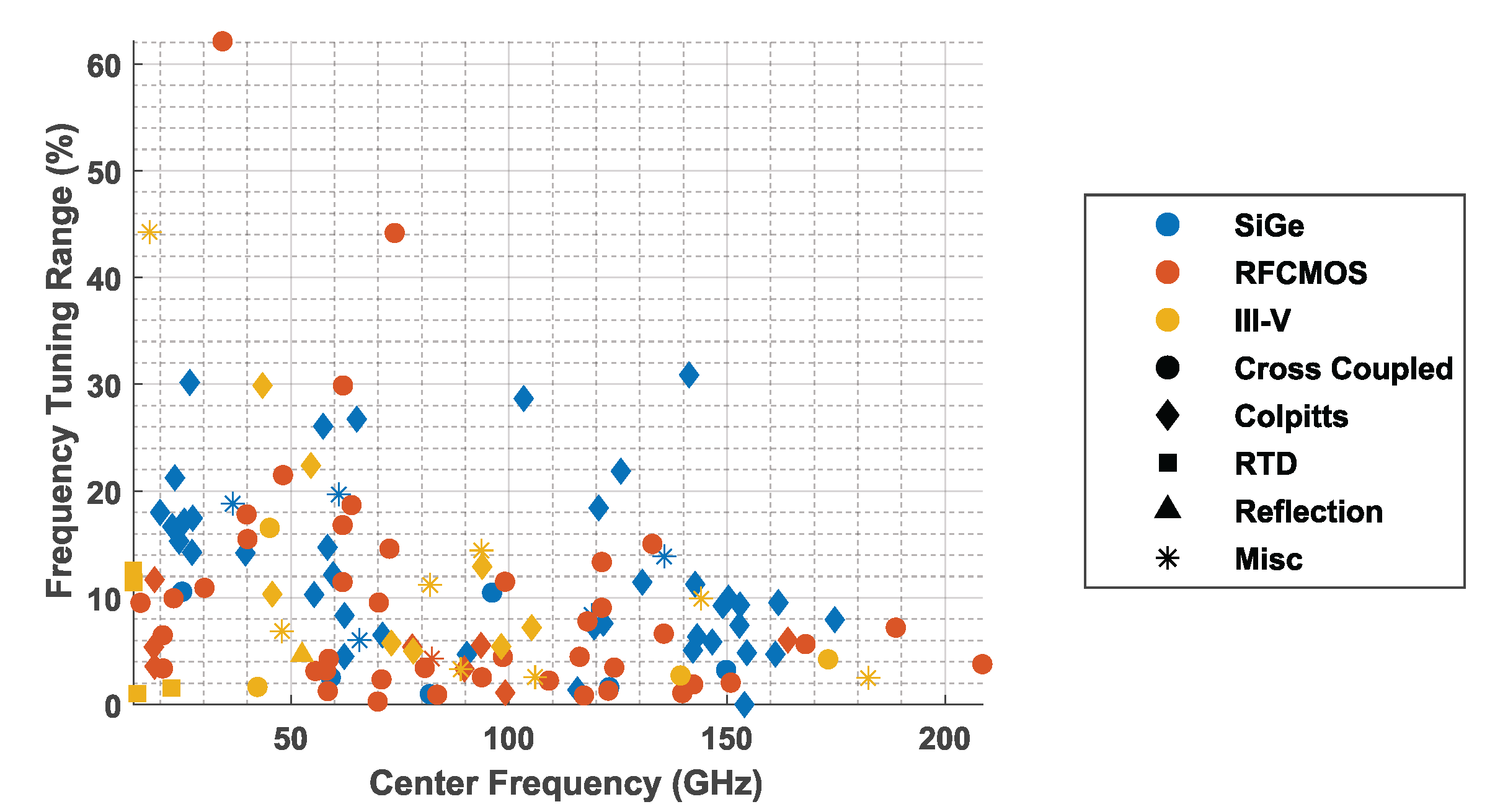

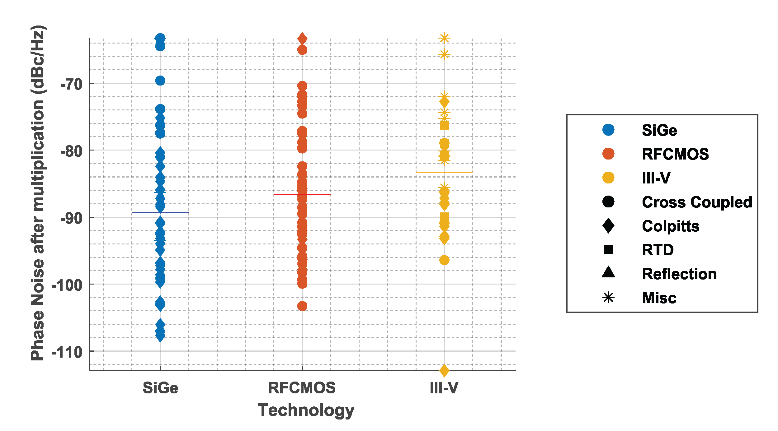
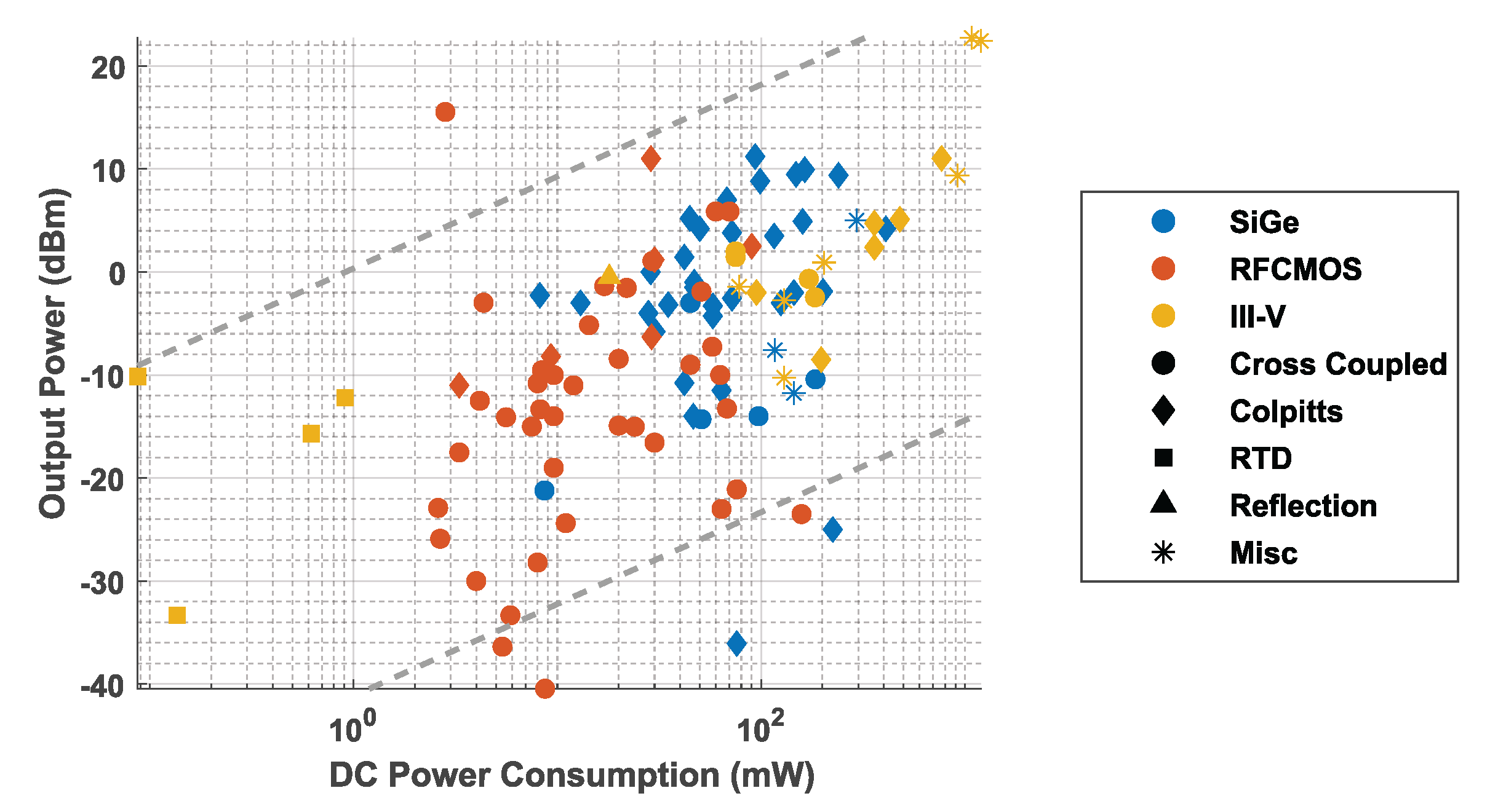
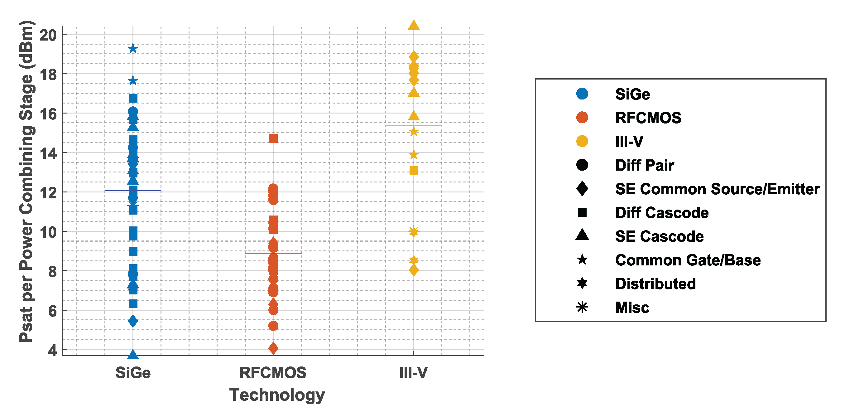
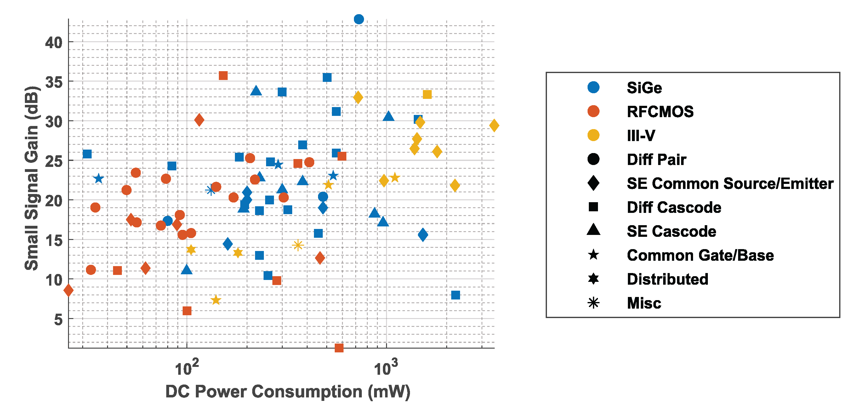
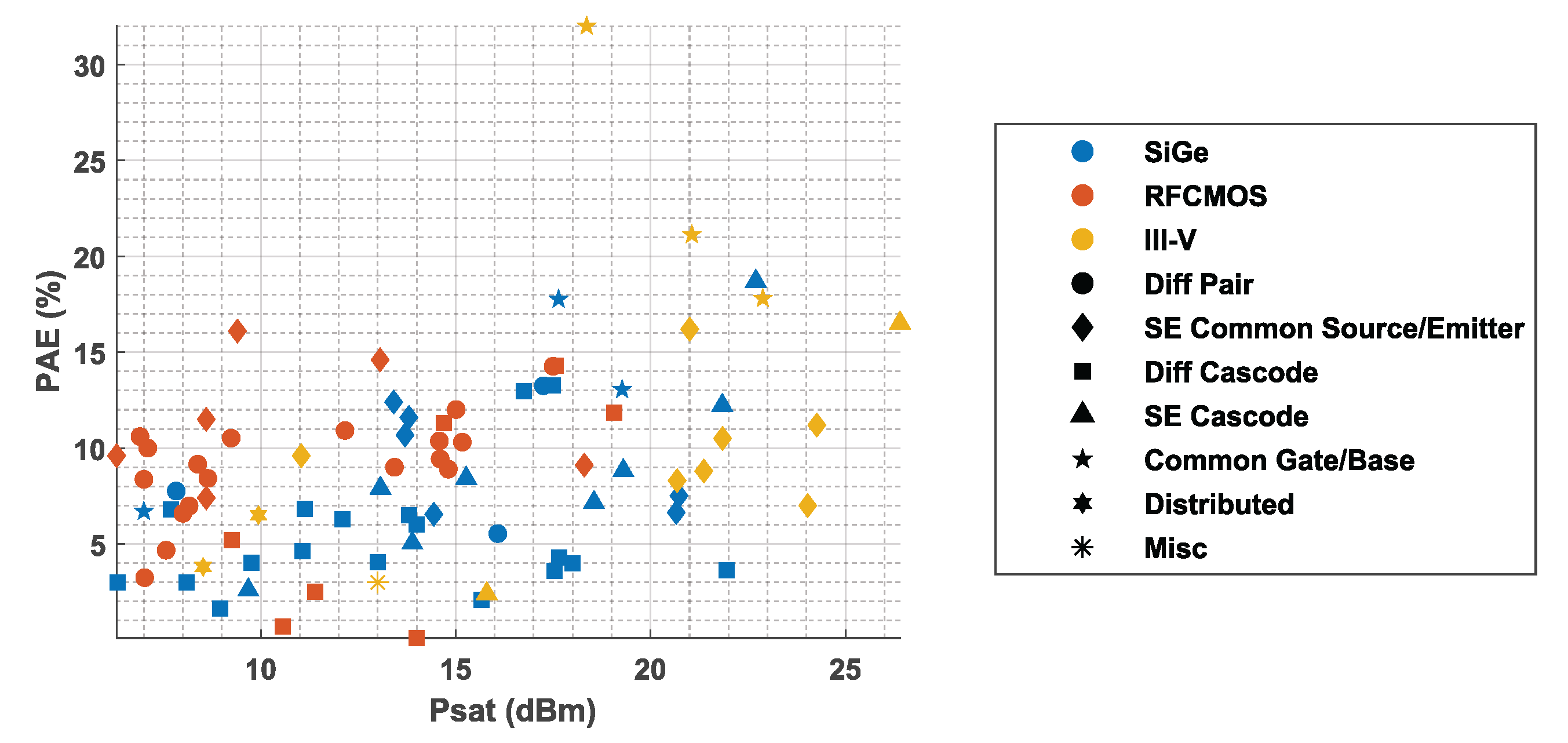
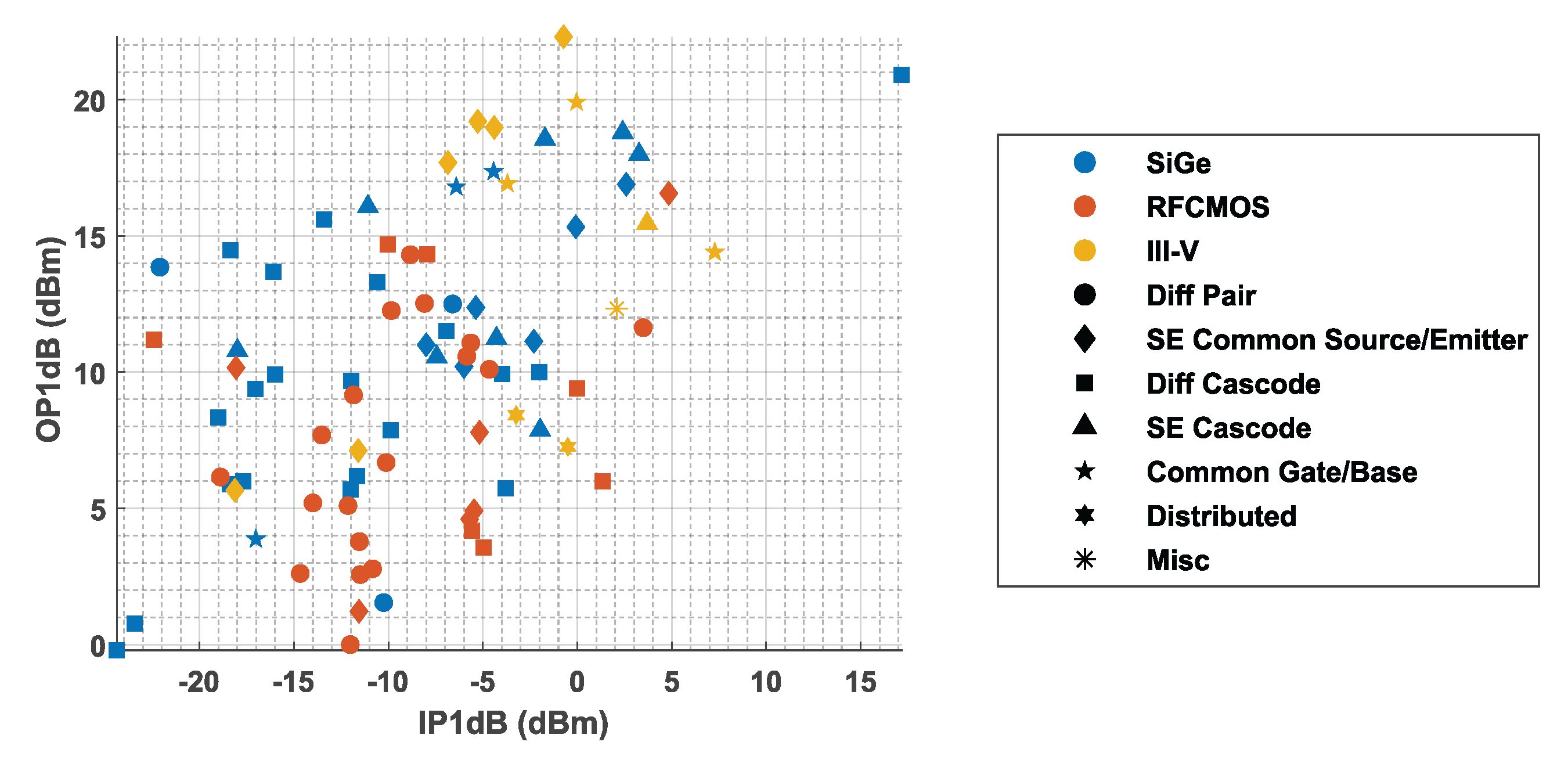
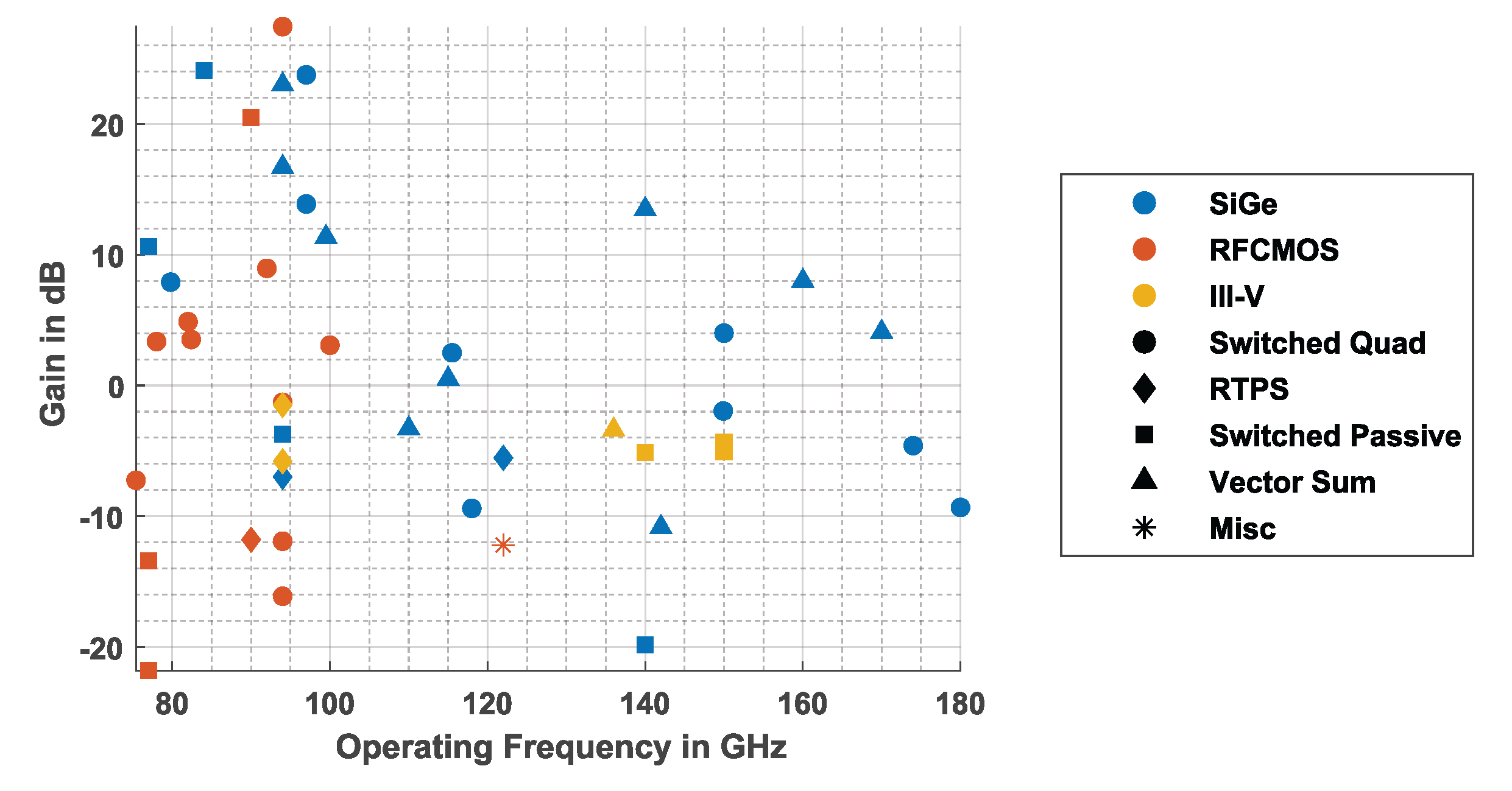
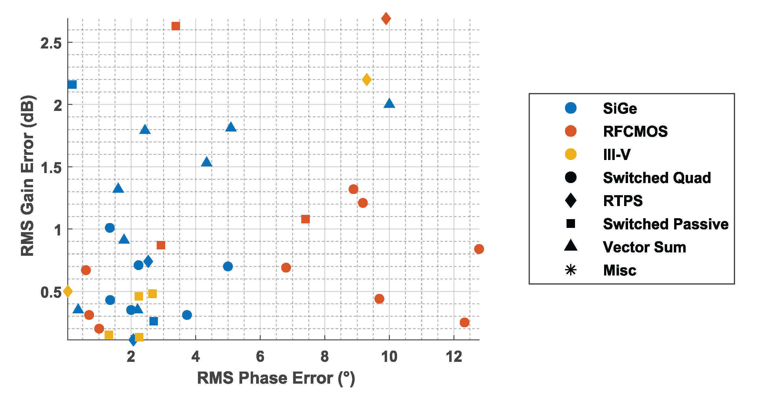
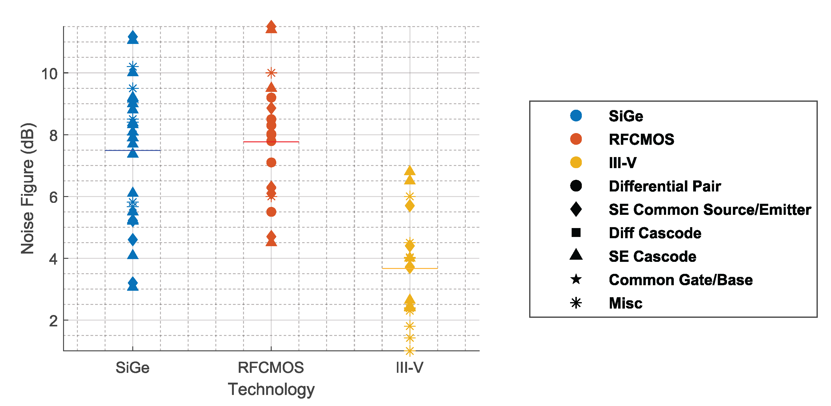
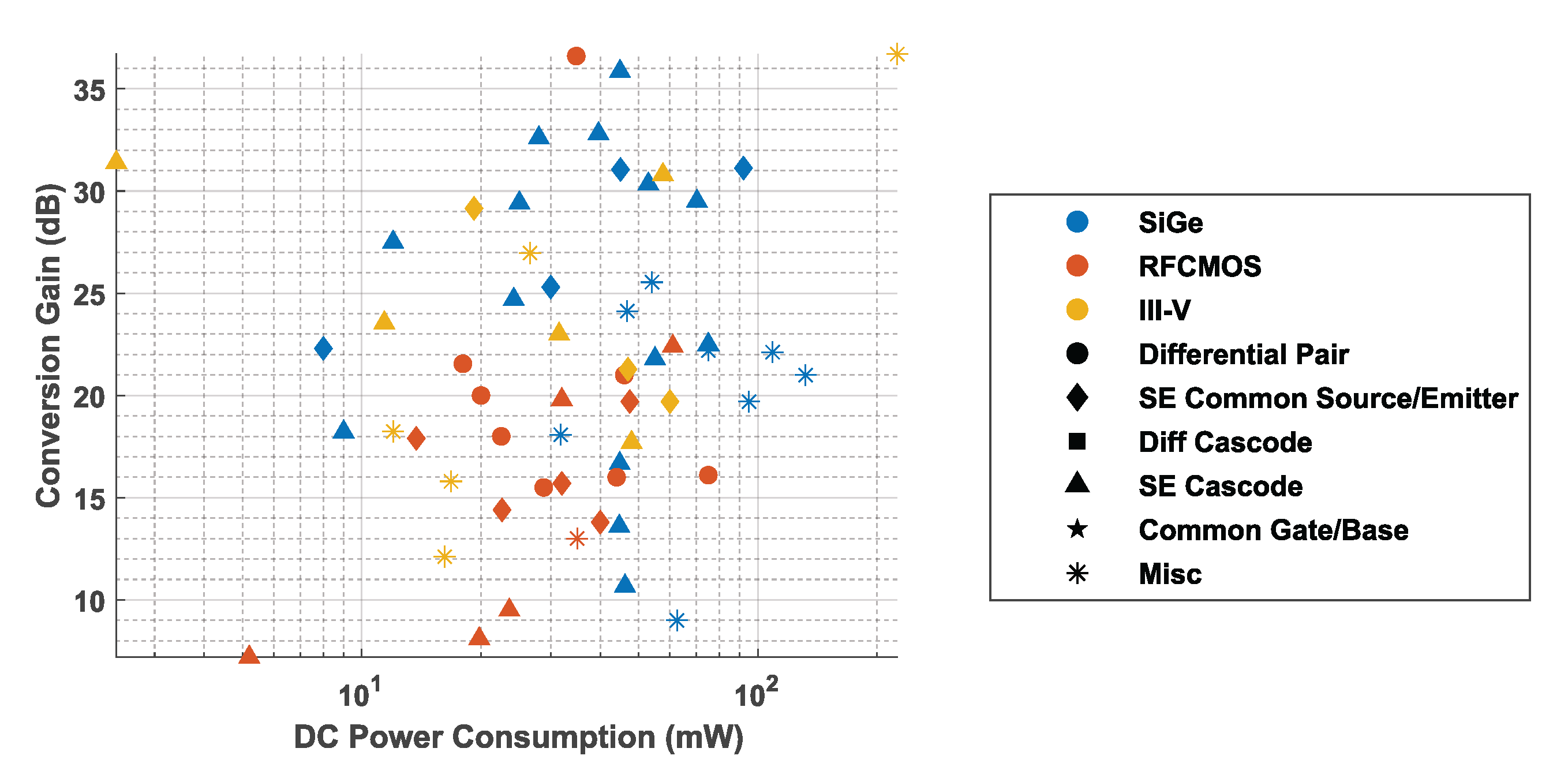
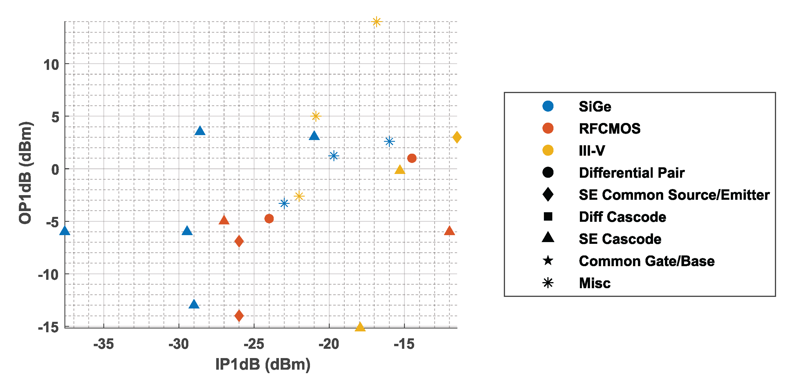


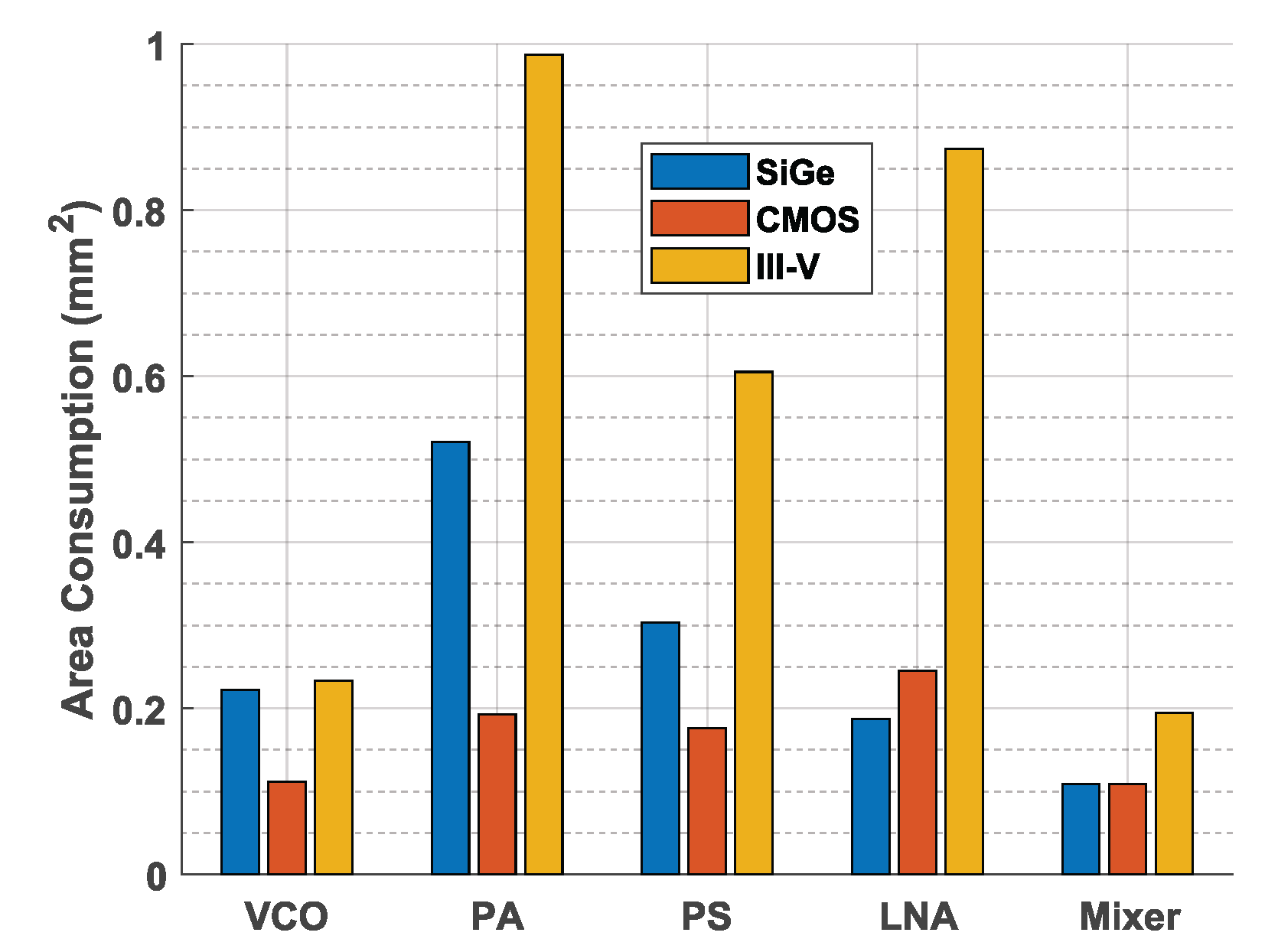
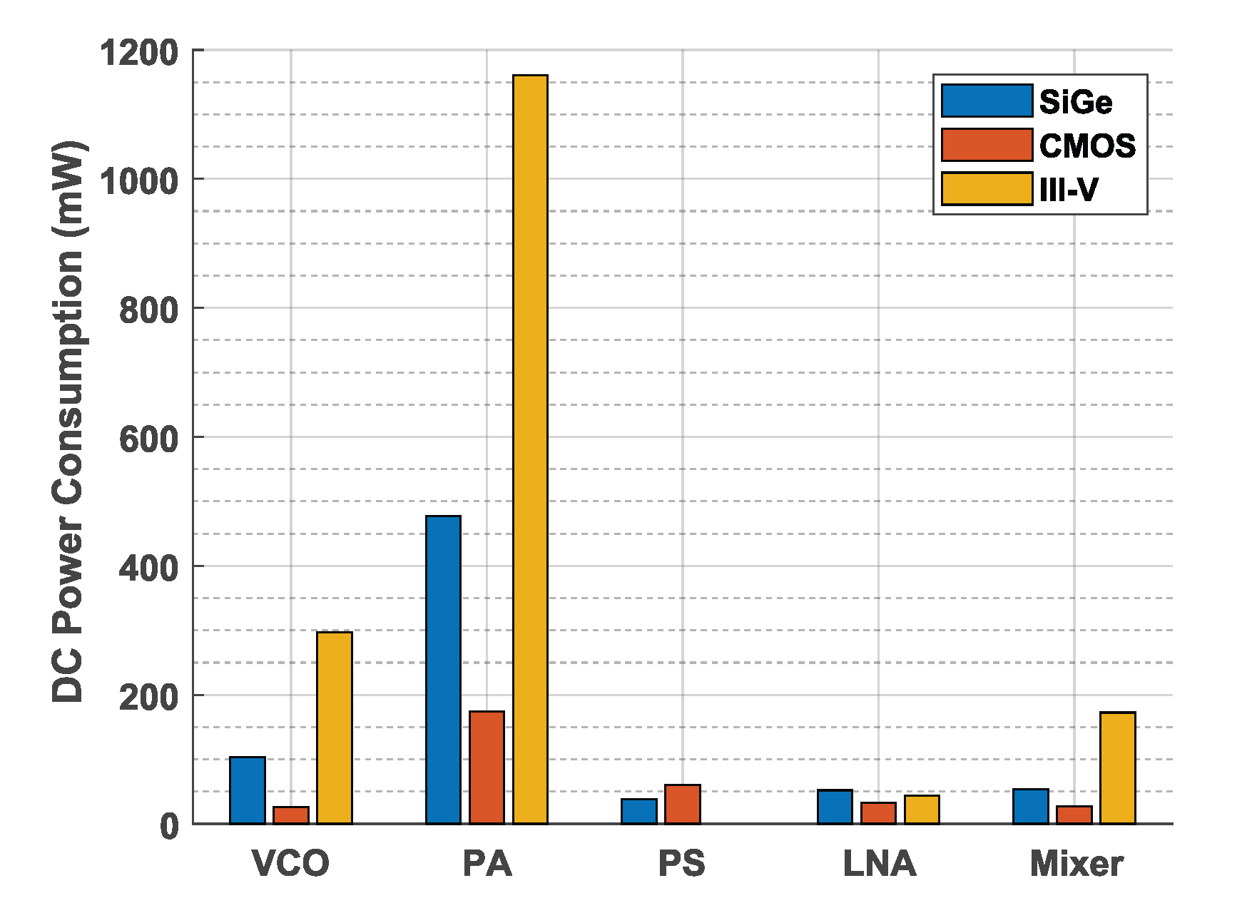
Publisher’s Note: MDPI stays neutral with regard to jurisdictional claims in published maps and institutional affiliations. |
© 2022 by the authors. Licensee MDPI, Basel, Switzerland. This article is an open access article distributed under the terms and conditions of the Creative Commons Attribution (CC BY) license (https://creativecommons.org/licenses/by/4.0/).
Share and Cite
Stadler, P.; Papurcu, H.; Welling, T.; Tejero Alfageme, S.; Pohl, N. An Overview of State-of-the-Art D-Band Radar System Components. Chips 2022, 1, 121-149. https://doi.org/10.3390/chips1030009
Stadler P, Papurcu H, Welling T, Tejero Alfageme S, Pohl N. An Overview of State-of-the-Art D-Band Radar System Components. Chips. 2022; 1(3):121-149. https://doi.org/10.3390/chips1030009
Chicago/Turabian StyleStadler, Pascal, Hakan Papurcu, Tobias Welling, Simón Tejero Alfageme, and Nils Pohl. 2022. "An Overview of State-of-the-Art D-Band Radar System Components" Chips 1, no. 3: 121-149. https://doi.org/10.3390/chips1030009
APA StyleStadler, P., Papurcu, H., Welling, T., Tejero Alfageme, S., & Pohl, N. (2022). An Overview of State-of-the-Art D-Band Radar System Components. Chips, 1(3), 121-149. https://doi.org/10.3390/chips1030009


