Abstract
Solar photovoltaic (PV) panels are the best solution to reduce greenhouse gas emissions by fossil fuel combustion, with global capability now exceeding 714 GW due to rapid technological advances in solar panels (SPs). However, SPs’ efficiency and lifespan remain limited due to the absence of advanced fault-detection systems, and they are prone to short circuits (SC), open circuits (OC), and power degradation. Therefore, this large-scale production requires reliable, real-time fault diagnosis to maintain panel performance. However, traditional diagnostic methods implemented using MPPT, neural networks, or microcontroller-based systems often rely on complex computational algorithms and are not cost-effective. So, this paper proposes a diagnostic system composed of six functional blocks to address this issue. The proposed system was initially verified using an Intel DE-10 Lite FPGA board. Once its functionality was confirmed, an ASIC design was proposed for mass production, offering a significantly lower implementation cost and reduced hardware complexity than prior methods. Different circuit designs were developed for each of the six blocks. All designs were created using Cadence software and TSMC 180 nm technology files. The basic components used in these designs include PMOS transistors with 300 nm channel length and 2 µm width, NMOS transistors with 350 nm channel length and 2 µm width, as well as resistors and capacitors. Differential amplifiers with a gain of 40 dB were used for voltage and current sensing from the SP. The chip activation signal generator circuit was designed with an adjustable frequency and generated 120 MHz and 100 MHz signals in this work. The decision-making block, Logic Driver Circuit, was innovatively implemented using a reduced number of transistors. A custom memory block with a reset switch was also implemented to store the fault value detected at the SP. Finally, the proposed ASIC was implemented for fabrication, which is highly cost-effective in mass production and does not require complex computational stages.
1. Introduction
The growing dependency on fossil fuels has expanded the focus on adopting renew- able energy systems. Among these resources, solar energy stands out for its abundance, sustainability, accessibility, and environmentally friendly nature. Since the first silicon solar cell patent was granted in the 1940s, they have consistently suffered from lower efficiencies, typically less than 1% [1]. This encouraged inventors to develop strategies and make solar panels more efficient. In 1954, Bell Laboratories created a solar cell with 4–5% efficiency; in 1963, they raised it to 6%. Soon after, many other strategies from additional laboratories proposed more efficient cells in the subsequent years, and in 2009, 25% efficiency was reached [2]. W. Shockley and Hans J. Queisser proposed an article in 1961 on the efficiency of a single-junction solar cell considering radiative recombination failure, which is also known as the Shockley–Queisser limit (SQ-L). The highest efficiency or the SQ-L of a single junction p-n solar cell is 30%. The practical lab efficiency for a single-junction solar cell is about 27%, which is less than the SQ-L. This SQ-L can also be developed for multi-junction solar cells; the SQ-L of such solar cells is set to be 86.8% [3]. Attaining a more efficient solar cell will help reduce the expense of an installed PV system. This remarkable growth reflects widespread deployment driven by cost reductions, improved efficiency, and strong policy support in countries like China, the United States and India, and across the European Union. As a result of these continuous advancements, the global installed capacity of PV systems has exceeded 714 GW [4].
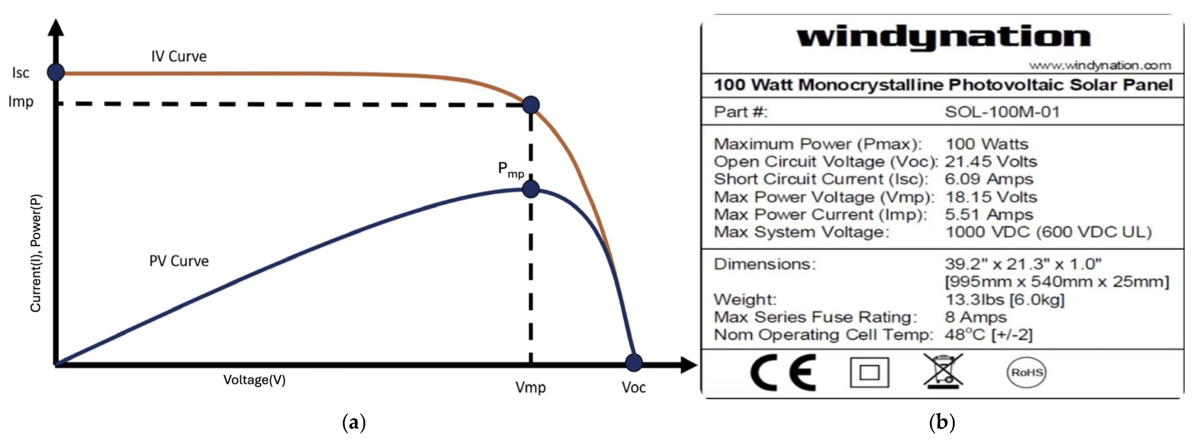
In Figure 1a, the plot shows the red solar panel’s (SP’s) voltage and current, and the related power curve is in blue [5]. A solar cell’s performance is defined by the key parameters affecting its efficiency. These are mainly short-circuit current (ISC), open-circuit voltage (VOC), and the maximum power point (MPP). The ISC results in the maximum current output because no external load is connected. At this point, the voltage across the cell is zero, and the cell provides its highest current. However, as the voltage increases, the current declines due to internal limitations, which leads us to the VOC [6,7,8]. The solar cell’s maximum voltage can be delivered under open-circuit (OC) conditions where no current flows through the SP. The cell has an MPP, also called PMP or Pmax, where it achieves the highest power output, which occurs at a specific voltage (VMP) and current (IMP) [9].
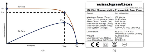
Figure 1.
(a) Solar panel voltage-current characteristics curve; (b) 100-watt panel specification.
Figure 1b shows an example of a commercial SP. According to the specifications of the 100-watt SP, the Pmax is 100 watts, which appears at the corresponding voltage and current values: VMP = 18.15 V and IMP = 5.51 A. The formula Pmax = VMP × IMP confirms this value [10]. In the specifications, the ISC is 6.09 A; any current above this value indicates a short-circuit (SC) condition in the SP [11,12]. Similarly, the VOC is 21.45 V, and from these values, the theoretical maximum power at VOC and ISC can be derived as VOC × ISC = 130.63 W. This yields maximum power at approximately 76.45% of this value. Any voltage beyond VOC suggests the SP is in an OC condition. Likewise, operating the cell at the MPP guarantees maximum efficiency from the SP, providing the most effective balance between voltage and current to maximize power. In contrast, operating the cell at ISC or VOC indicates a malfunction, as these conditions cause the SP to be short-circuited or open-circuited.
The proposed work aims to design a chip that can detect the occurrence of an OC or SC in the SP and indicate if the SP is experiencing an issue. Application-Specific Integrated Circuits (ASICs) and Field-Programmable Gate Arrays (FPGAs) are semiconductors that suit various electronics objectives [11]. FPGAs are reprogrammable appliances that provide flexibility to change the device functionality as per requirements; ASICs are custom-designed for specific uses, delivering high performance and efficiency [13]. By understanding the differences between these devices, designers can make decisions that best suit their project requirements and constraints [14,15].
As shown in the Table 1, FPGA is a device that can be reprogrammed to implement various digital circuits and functions. It consists of programmable 2–5 million logic blocks. It interconnects, allowing for the configuration of a wide range of digital circuits, from simple logic gates to complex digital signal processing systems [16]. FPGA programming usually uses a hardware description language (HDL), such as VHDL or Verilog [17]. These languages allow designers to describe the desired functionality of the device. The HDL code is converted into a bitstream, which is loaded onto the FPGA. This process can be repeated to update or modify the FPGA’s functionality, providing a high degree of design adaptability. There are different kinds of FPGAs available on the market. For example, Microchip’s PolarFire, SmartFusion, and IGLOO series; Intel’s Agilex, Stratix, and Arria series; and AMD’s Virtex UltraScale+ series. Among these, the DE10-Lite board from Intel was used for this project [18].

Table 1.
Comparison between FPGA and ASIC used in this work.
ASICs are technical semiconductor devices and circuitry designed to perform a par- ticular function or operation. They are tailored to meet the needs of a special application, giving optimized performance and power efficiency [19]. They are typically used in high- volume products where improved performance and lower power consumption can justify the price of custom design. Plenty of tools are available on the market for ASIC design and implementation. Cadence Design Systems and Synopsys are major companies offering a comprehensive suite of tools for a full ASIC design flow. This work used the Cadence Virtuoso suite with the TSMC 180 nm technology.
So, in this paper, we suggested a program that tests the SP diagnosis circuit through FPGA; once the functionality test was successful, we proposed the ASIC development circuitry for the SP diagnosis. This enables us to assess whether the ASIC’s functionality meets our requirements for the Solar Panel Diagnostic (SPD) system. Moreover, we can reduce the price by mass-producing the same chip, which can be mounted alongside the SP.
2. Prior Art
PV fault detection has highlighted the need for accuracy and real-time responsiveness in solar panel monitoring systems. Maximum PowerPoint Tracking (MPPT) techniques have been extensively researched to maximize energy harvesting. Traditional methods such as Incremental Conductance (INC) and Perturb and Observe (P&O) achieved 94.3% and 97.6% accuracy, respectively, while their hybrid versions, INC-PSO and P&O-PSO, reached a performance level of 99.6%. Artificial intelligence (AI)-based algorithms, including Fuzzy-PSO, artificial neural networks (ANNs), Adaptive Neuro-Fuzzy Inference Systems (ANFIS), and ANN combined with PSO, have also demonstrated high accuracy levels ranging from 98% to 98.8%. Although these intelligent algorithms are becoming essential for PV optimization, they require significant computational resources [20].
The MPPT systems developed by Solórzano and Egido [11] introduced an economical diagnostic method capable of detecting faults of different types without applying environmental sensors like irradiance or temperature. This method is particularly apt for small PV systems only. Another technique by García et al. [21] used microcontrollers and current sensors in SCADA-based systems to analyze open-circuit voltage (VOC) and short-circuit current (ISC) manners. The system achieved error rates for voltage and current less than 1% and 2%, respectively. While these approaches are practical, they require external sensors or embedded processors, increasing system complexity and cost.
Artificial neural network approaches have also been proven to help classify PV faults. Hwang et al. presented an ART2 and Modular Neural Network-based hybrid diagnosis system. This method achieved 100% classification with inputs like VOC and duty cycle, designed explicitly for solar streetlight applications. Another diagnostic system tested panel aging with intrinsic parameters such as photocurrent, shunt capacitance, and diode attributes [22]. These intelligent systems rely on complex computations and sensor-based inputs, which increase hardware requirements and limit their suitability for low-power or large-scale PV deployments.
Machine learning remains a top approach for PV fault detection. Dhanraj et al. [23] reviewed ML-based and sensor-based versions. This approach is used to detect faults such as open circuits, diode faults, and partial shading. Approaches combining thermal imaging and Convolutional Neural Networks (CNNs) achieved a high (99.74%) accuracy and an F1 score of 0.9818 in tests. However, these intelligent approaches typically require large datasets, high computational resources, and real-time sensor inputs, making them less practical for PV installations.
Unlike prior sensor-based and ML-driven approaches, the proposed ASIC-based system offers real-time fault detection using compact hardware blocks without external sensors or computation. It is designed with TSMC 180 nm CMOS technology and provides a low-power, cost-effective solution suitable for large-scale PV panel integration.
3. Proposed System Architecture
Figure 1b shows that the 21.45 V SP specification suggests that the VMP is 18.15 V. The SP is considered to be in an OC state when the output voltage exceeds the range of 19 V to 21 V. In the same way, 6.09 A is the Isc for the above-shown solar panel, and the Imp for the solar panel is 5.51 A. So, if the current occurs above 5.51 A to 6.09 A, it is considered a short-circuited solar panel. Since the proposed technique works at a supply voltage of 3.3 V, it is necessary to step down the solar panel voltage to a level compatible with the system [24]. A voltage divider circuit is employed to scale the input voltage down to a range that the technique can safely process.
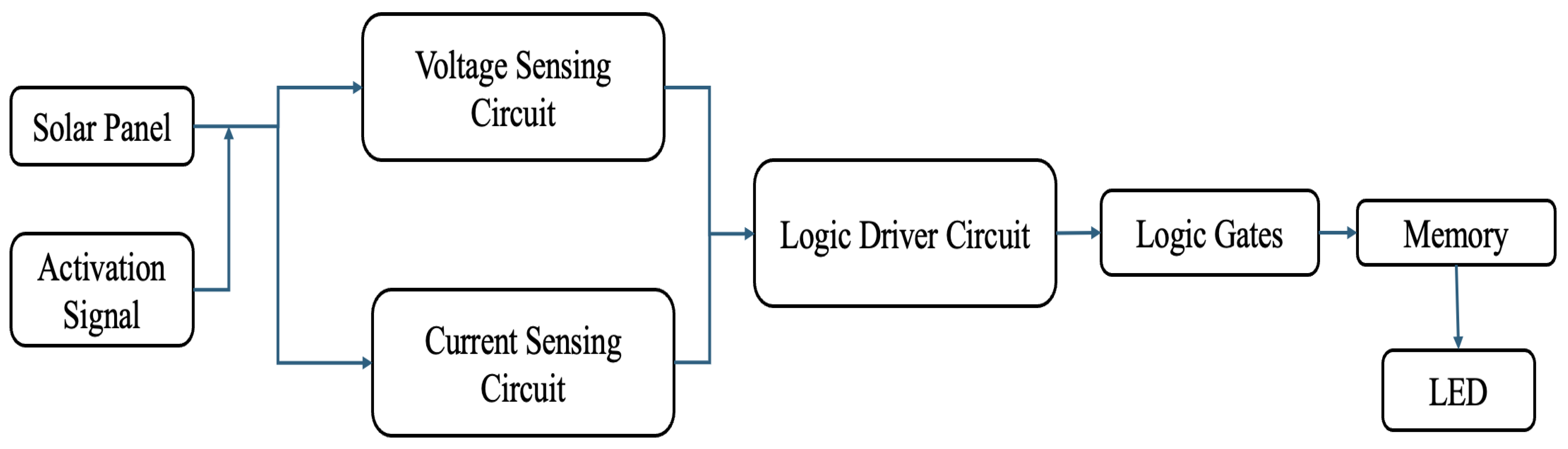
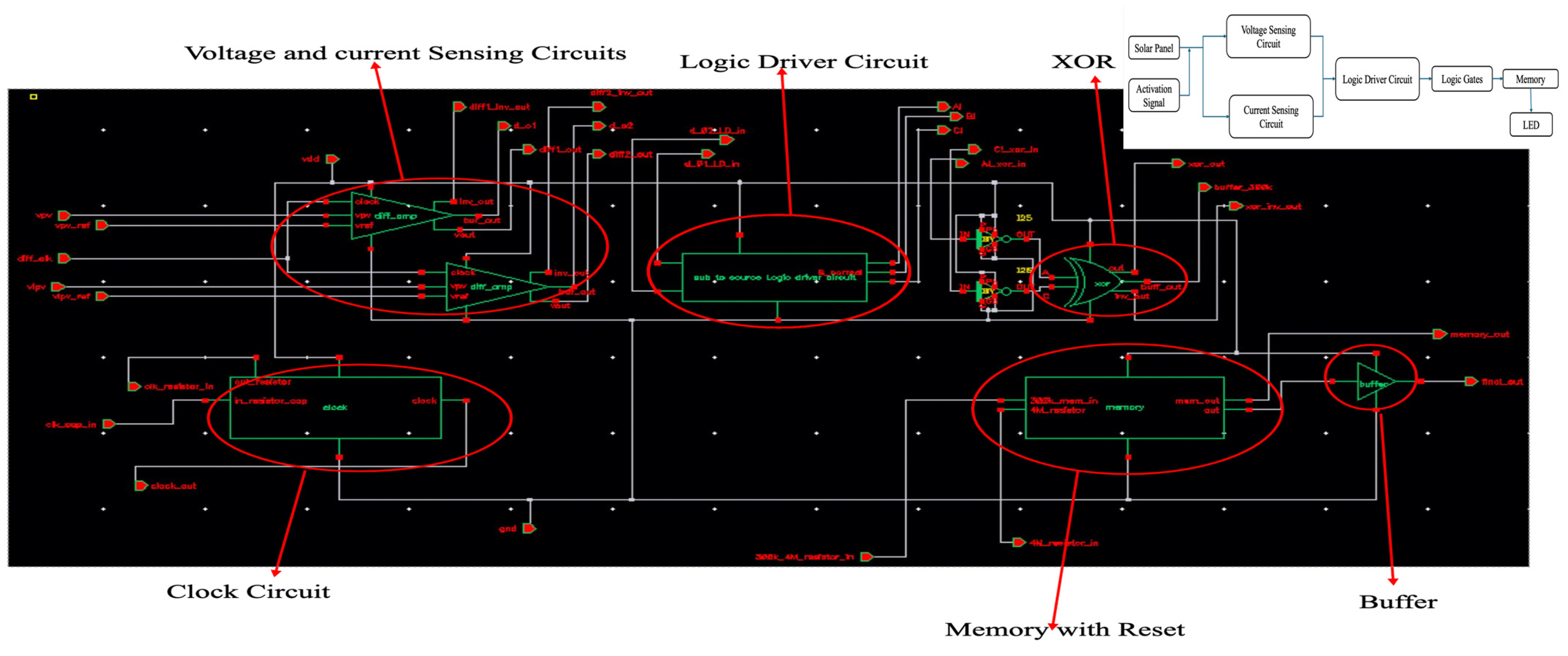
From an SP, we can derive the voltage (Vpv) and current (Vipv) to determine whether the solar panel is short- or open-circuited, as indicated in Figure 1a. Therefore, the proposed system is developed to detect both Vpv and Ipv from the SP utilizing a voltage-sensing circuit (VSC) and a current-sensing circuit (CSC), as shown in the block diagram. As shown in the Figure 2, the outputs from the VSC and CSC are integrated into a logic driver circuit (LDC) block that develops unique signals to decide whether the SP is experiencing an SC or an OC or working normally. The LDC further processes these signals, providing an XOR logic gate that outputs an errored signal when an SC or OC condition is detected. A memory unit at the output ensures the LED indicator stays ON until the noticed fault is fixed. A clock activation circuit is used to turn on the whole circuit. This work proposes a code implementation for the SPD FPGA, as suggested by the block diagram. ASIC circuitry is also implemented for each block diagram element [25].
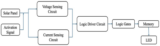
Figure 2.
Block diagram of the proposed system including VSC, CSC, LDC, logic gate, and memory.
4. FPGA-Based Verification for SPD System
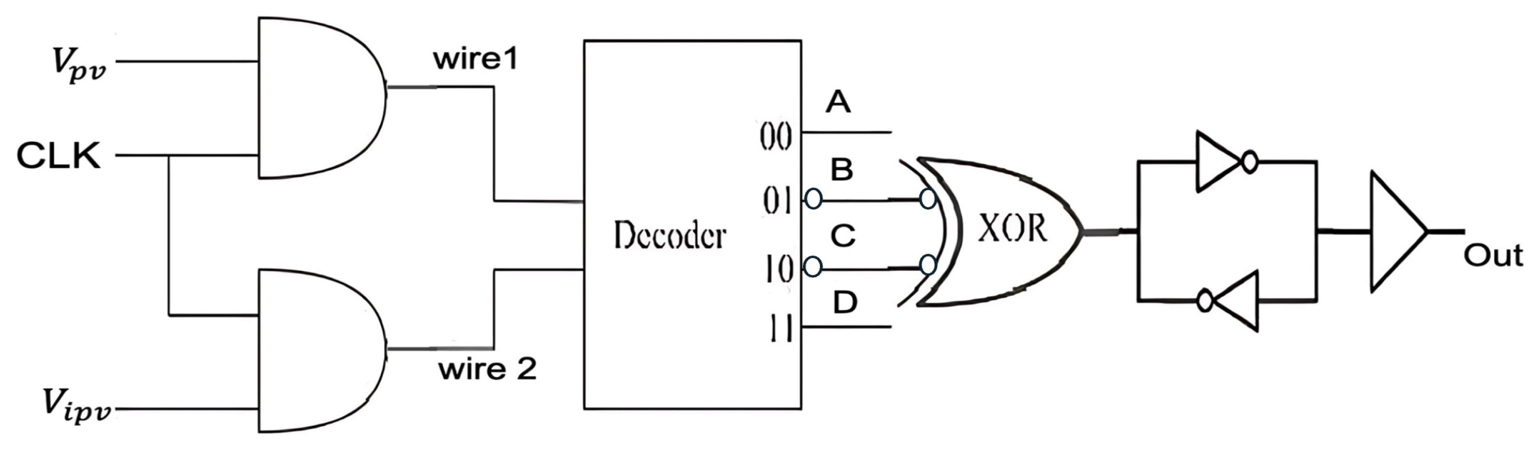
To implement code in an FPGA for the SP functionality test, a circuit with AND gates was taken for VSC and CSC, a decoder was taken for LDC, and an XOR gate was proposed for the logic gate. In two inputs for the AND gate, one input is given to Vpv/Vipv and another to the circuit activation system. AND gates are chosen for VSC and CSC because whenever the logic 1 (HIGH) or logic 0 (LOW) voltage comes from the solar panel, it will be projected at the output end when the circuit activation signal is also logic 1. The output is zero for both conditions of 1 or 0 of the SP when the circuit activation signal is 0. The VSC signal output is named wire 1, and from the CSC it is given as wire 2. This signal was given to the LDC, which is nothing but a decoder, and based on the signal from VSC and CSC, the LDC determines the output. LDC has four output signals for two inputs: A, B, C, and D [26]. If the signal from wire 1 and wire 2 is logic 0 and 0, then Decoder output signal A will give a logic 1 signal as the output. The rest of the signal outputs B, C, and D give logic 0. In the same way, for 01 from wire 1 and wire 2, the B signal gives 1 for 10, the C signal gives HIGH output, and for 11 combinations, the D signal gives 1. A decoder-based LDC was chosen for its simplicity and ability to map two input signals to four unique states. Compared to multiplexers or combinations of logic gates, the decoder offers a more compact and efficient solution with fewer transistors, making it ideal for both FPGA testing and ASIC implementation.
Among A, B, C, and D signals, signals B and C correspond to SP’s short and open circuits. So, among these two, any signal HIGH needs to be detected by the next stage of the circuit. So, the XOR gate was used to detect the signal and give a logic 1 signal if B or C is logic 1. After XOR, a back-to-back inverter is connected to hold the output value. Figure 3 below shows the circuit diagram implemented and should be uploaded to the FPGA.
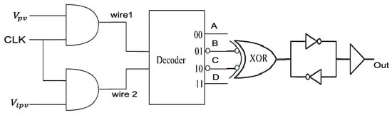
Figure 3.
FPGA implementation circuit diagram using the AND gate for VSC and CSC, the decoder for LDC, the XOR gate, and the output back-to-back inverter for SP functionality testing.
4.1. Code Implementation
Table 2 shows all outputs for each input combination; as shown in the table, outputs B and C are the short and open conditions [27]. The HDL code below implements and tests the proposed circuit using the Intel DE-10 FPGA board. In the code, LED2 is assigned to decoder output A, LED3 is assigned to B, LED4 is assigned to C, LED5 is assigned to D, and LED6 is assigned to the final output.
Table 2.
Logic combinations with decoder and memory output.
| //Step 1: Read Inputs Input Vpv, Vipv, CLK |
| //Step 2: Generate gated signals wire1 = AND(Vpv, CLK) wire2 = AND(Vipv, CLK) |
| //Step 3: Invert intermediate signals NotWire1 = NOT(wire1) NotWire2 = NOT(wire2) |
| //Step 4: Create condition logic Temp1 = NotWire1 AND NotWire2 Temp2 = NotWire1 AND wire2 Temp3 = wire1 AND NotWire2 Temp4 = wire1 AND wire2 |
| //Step 5: Output logic from decoder A = NOT(Temp1)//No input from SP (idle) B = NOT(Temp2)//Short Circuit (SC) C = NOT(Temp3)//Open Circuit (OC) D = NOT(Temp4)//Normal panel condition |
| //Step 6: Output states to LEDs LEDR0 = wire1//Voltage line status LEDR1 = wire2//Current line status LEDR2 = A//Idle or no signal LEDR3 = B//SC detected LEDR4 = C//OC detected LEDR5 = D//Normal condition |
| //Step 7: Fault detection using XOR logic XORout = B XOR C |
| //Step 8: Memory latch to hold fault state Buff1 = NOT(XORout) Buff2 = NOT(Buff1) LEDR6 = Buff2//Latched output (1 if SC or OC occurred) |
| END |
4.2. SPD System Functionality Test Results
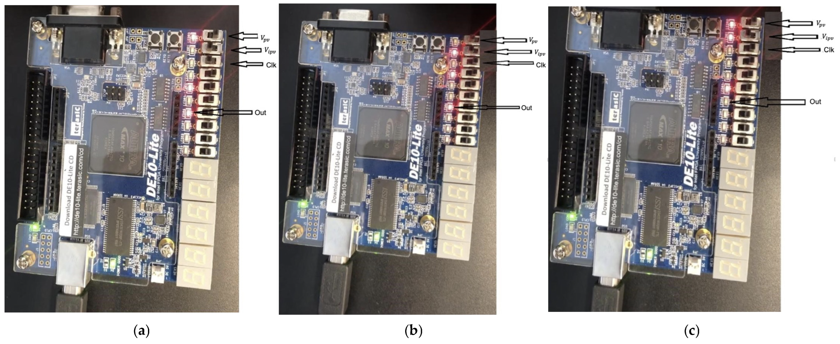
Once the HDL code is uploaded to the FPGA, the FPGA will work as the proposed circuit. Also, the proposed work sought to observe the effects of various combinations of inputs on the FPGA board using switches. If the switch is on, it is considered to be logic 1. We utilized three switches for three inputs, as shown in the figure.
From Figure 4a, when the inputs Vpv and Vipv are set to 01, the output of SPD indicates a defect 1 signal at LED6. Likewise, in Figure 4b, the output signal indicates a high of 1 for A = 0, B = 1, and D = 1 inputs. This indicates a short-circuit condition in the solar panel. From Figure 4c, when the inputs A and D are set to 00, the decoder output indicates no defect, as the LED6 is OFF. So, the results from the FPGA confirm that the proposed circuit behaves as an SPD system and can be utilized to detect the SC or OC of SP.
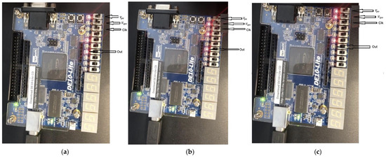
Figure 4.
(a) FPGA LED6 displays defect detection out = On (for Vpv and Vipv Inputs: 01); (b) Y= On (Vpv and Vipv Inputs: 10); (c) FPGA LED6 Off (A and D switches are logic 0).
5. ASIC Based Implementation
After completing the SPD functionality test with the FPGA, we can move forward with designing the implementation of the ASIC. All circuits were designed using Cadence Virtuoso, utilizing the TSMC (Taiwan Semiconductor Manufacturing Company, Hsinchu City, Taiwan, Republic of China) 180 nm technology library for component selection [28]. All the circuits were designed using the 3V functional devices, which operate reliably at 3.3 V. All the designs utilize basic components, such as PMOS, NMOS transistors and resistors [29].
For the ASIC implementation, the proposed circuits for each block from the block diagram are shown in Figure 2. This work proposed a differential amplifier as a comparator for VSC and CSC. Even though we used digital NAND circuits for VSC and CSC in FPGA tests, in real-time, the SP output comes in an analog form, not digital [30]. The analog component differential amplifier is designed to detect these analog signals. These analog comparators convert the analog signal to digital. These differential amplifiers can be activated using the standard clock signal. A clock circuit was proposed for activation clock signal generation. The digitalized signals from the VSC and CSC are given to the logic LDC circuit, and then the B and C signals are given to the XOR circuit. A custom memory element with a switch is also proposed in this work to hold the value [31].
Figure 5 illustrates all the symbolized components connected according to the block diagram in Cadence Virtuoso. All the corresponding input and output pins are taken out to check the signal status at every circuit stage. The following sections explain each component in the circuit individually.
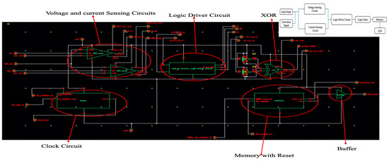
Figure 5.
Complete circuit schematic with symbolized clock circuit, VSC, CSC, LDC, logic gate, memory, and I/O pins designed in Cadence Virtuoso.
5.1. Voltage Sensing and Current Sensing Microcircuits
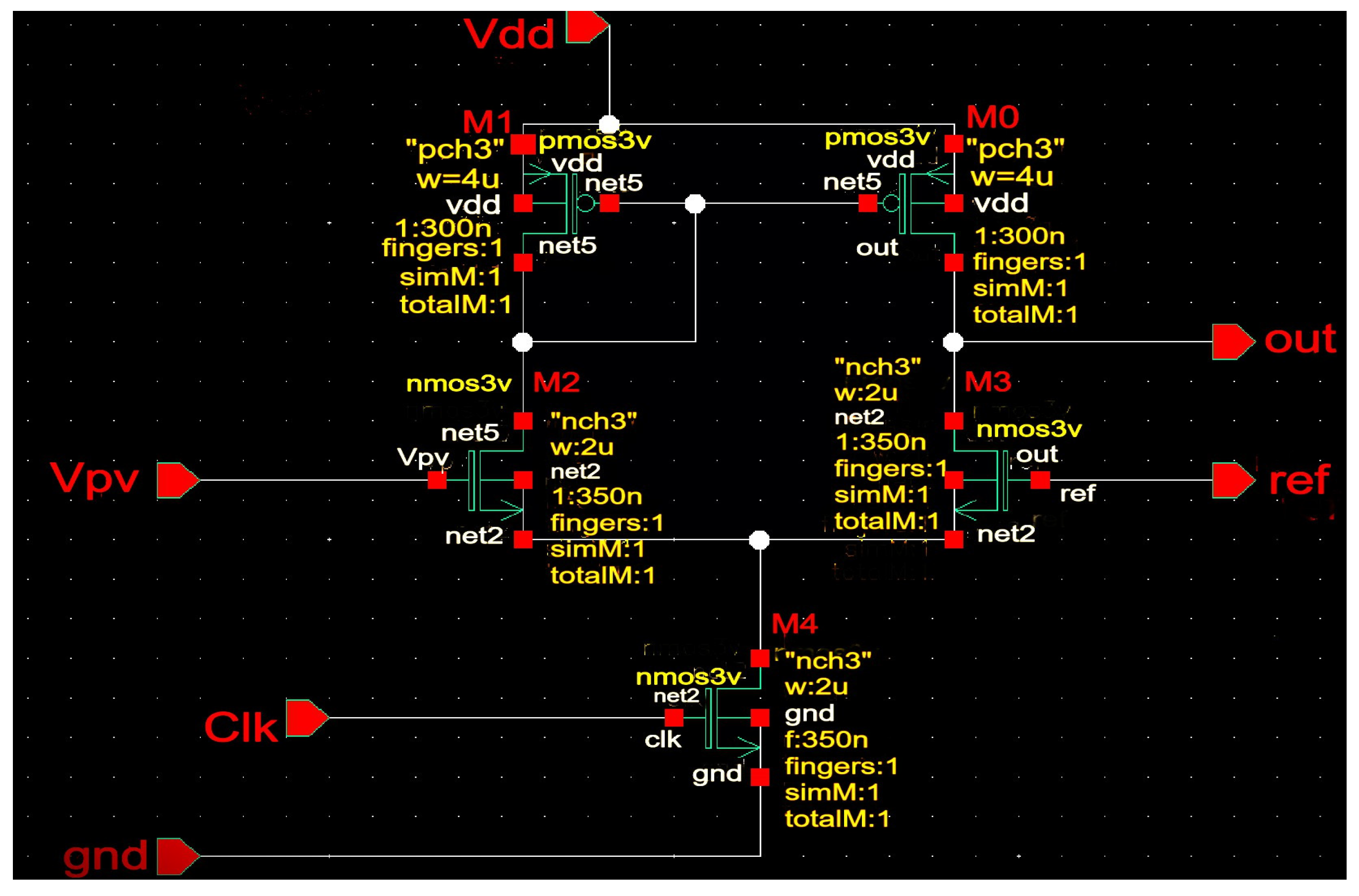
A Differential Amplifier (DA) is utilized for the VSC and CSC design. VSC and CSC compare the diagnostic circuit’s measured voltage and current from SP with the reference values. If the voltage from the SP overreaches the reference voltage, the DA instantly pulls the signal to logic 1, saying that the SP is open-circuited. Similarly, if the current from the SP exceeds the reference safe current level, the CSC pulls the signal to logic high, showing an SC condition. Thus, the DA is a comparator, delivering the corresponding digitalized output to the next stage, LDC. The output of the DA is expressed as follows:
The PMOS devices in the DA are developed with a width of 4 µm and a channel length of 300 nm, while the NMOS devices are designed with a width of 2 µm and a channel length of 350 nm. A DA was chosen because it has three input pins; one can be used as a reference, and the other can receive input from the solar panel’s output [32].
As shown in the Figure 6, The third pin is the circuit activation pin, which can be connected to the clock circuit. When the clock is HIGH 1, the circuit starts working, and input values are compared to reference values and digitalization. The comparator ensures that a slight difference between Vin and Vref results in a fast output transition, reducing signal delay [33].

Figure 6.
Differential amplifier circuit diagram acting as a comparator with PMOSs with 4 µm and a channel length of 300 nm, NMOSs with 2 µm width and a channel length of 350 nm.
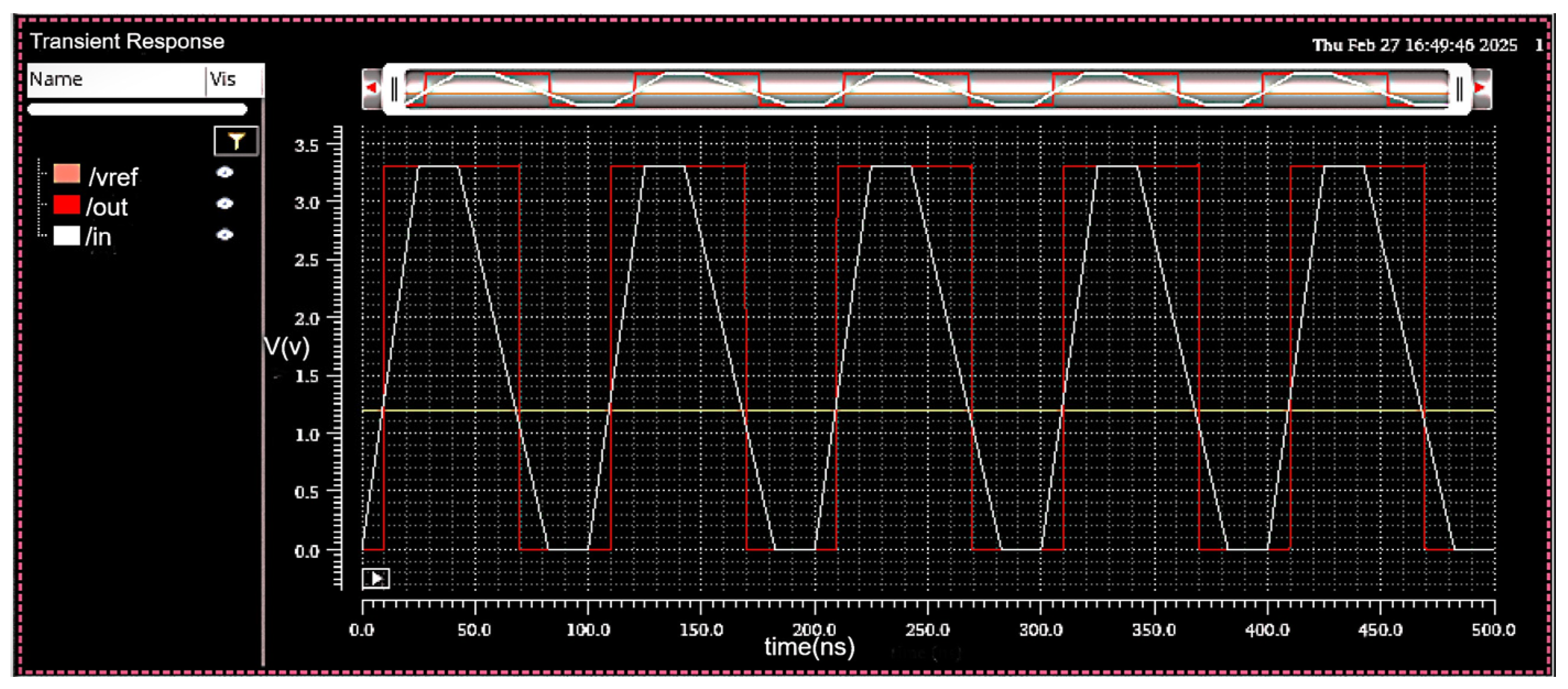
Since the signal from the solar panel is analogue, a triangular waveform is assumed to be a representative signal that can be produced for simulation and analysis. As shown in Figure 7, the DA successfully operates the 25 ns rise-time signal to logic HIGH 1 when the input signal crosses the reference voltage level and instantly pulls it to logic low when the triangular signal falls below the reference [34]. A 25 ns rise time corresponds to a frequency of 40 MHz, clearly indicating that the system can efficiently work at 40 MHz or higher. The designed DA provides a voltage gain of approximately 40 dB, which corresponds to a linear voltage gain of 100 (using the formula Gain (dB) = 20 log10(gain)). The amplifier also exhibits a bandwidth of 5 MHz, allowing it to respond quickly to signal transitions, which is more than adequate for solar panel diagnostics, where signal changes occur relatively slowly. Additionally, the input offset voltage is measured to be around 5 mV, indicating good transistor matching and ensuring the accurate detection of short-circuit (SC) or open- circuit (OC) conditions. The digitized result from the DA is then ready to be delivered to the next stage of the circuit, the LDC, for further analysis.
Figure 7.
The digitized output of the differential amplifier in response to a triangular waveform input.
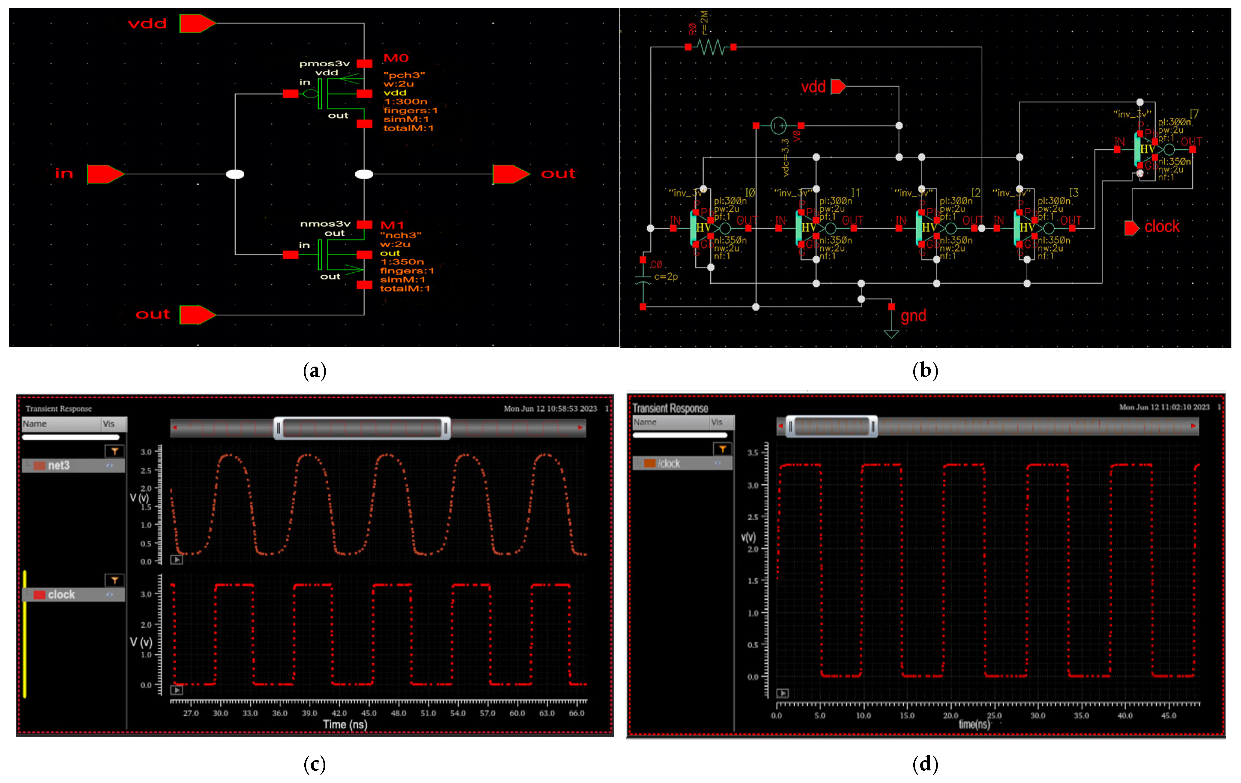
5.2. Activation Clock Signal Circuit
One of the DA inputs is connected to the clock circuit output. The DAs work only when the clock signal is HIGH or logic 1. The clock signal is designed using a series of connections to inverter circuits, one feedback resistor, and the capacitor at the input, as shown in Figure 8b design. The inverter is designed using one PMOS and one NMOS connected, as shown in Figure 8a, and converted to a triangle symbol to connect as a string. The inverter circuit inverts the input signal to the opposite value, such as logic zero, which can be converted to logic 1. Similarly, logic 1 can be converted to logic 0 [33].
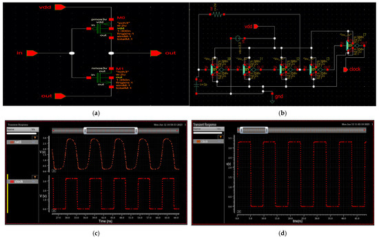
Figure 8.
(a) Inverter circuit diagram. (b) Clock generation circuit using feedback R and C configuration. (c) Output waveform with 2 MΩ and 3 pf (120 MHz). (d) Output waveform with 2 MΩ and 5 pf (100 MHz).
The clock is the signal that has a HIGH 1 signal and a LOW 0 signal alternately. This continues repeatedly. The time period is the combination of high and zero logic periods. Initially, the clock input has the 0 value that can be converted to logic 1 at the output, and then, by virtue of the feedback resistor, the capacitor will charge to logic 1 and make the input logic 1. Logic 1 will be converted to 0 at the output, and the capacitor will be discharged. This process will be performed again and again. The time period of the clock signal can be determined by the resistor value (R) and the capacitor value (C). The time period of the generated output can be given by the formula T = RC, and the formula f = 2 1 gives the frequency of the generated output. The frequency can also be varied by changing the values of R and C. For the above-suggested circuit, the combination of the resistor 2 MΩ and the capacitor 3 pF gives a time period of 8 ns and a frequency of 120 MHz. For the combination of the 2 MΩ resistor and the 5 pF capacitor, the output wave time period is 10 ns and 100 MHz, as shown in Figure 9. Based on the requirement, we can activate the SPD circuit using the clock generation circuit.

Figure 9.
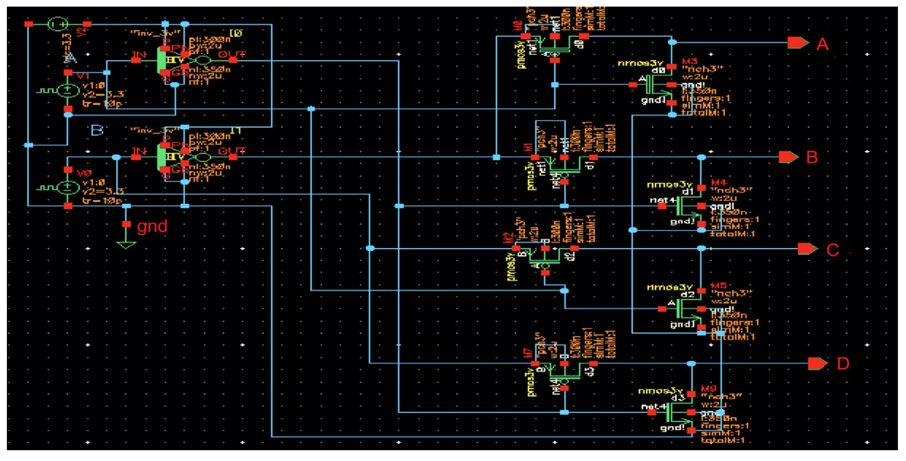
Proposed 12-transistor LDC.
5.3. Logic Driver Circuit and Logic Gate
Once the digitalized signal from the DA is obtained, the LDC analyzes the SP state by processing the outputs from both the VSC and CSC. The LDC is developed to generate four types of signals, providing individual outputs for each possible combination of high and low states [34]. A 2 × 4 decoder can be used for this purpose. However, the decoder has 22 transistors, so to make the chip more compact, this work has proposed a circuit that acts the same as the decoder, which has 12 transistors, including 4 transistors used for two inverter circuits. Figure 9 shows the proposed 12-transistor Logic Driver Circuit [35]. This difference in the number of transistors yields very notable differences in area, power consumption, and manufacturing costs on a large scale.
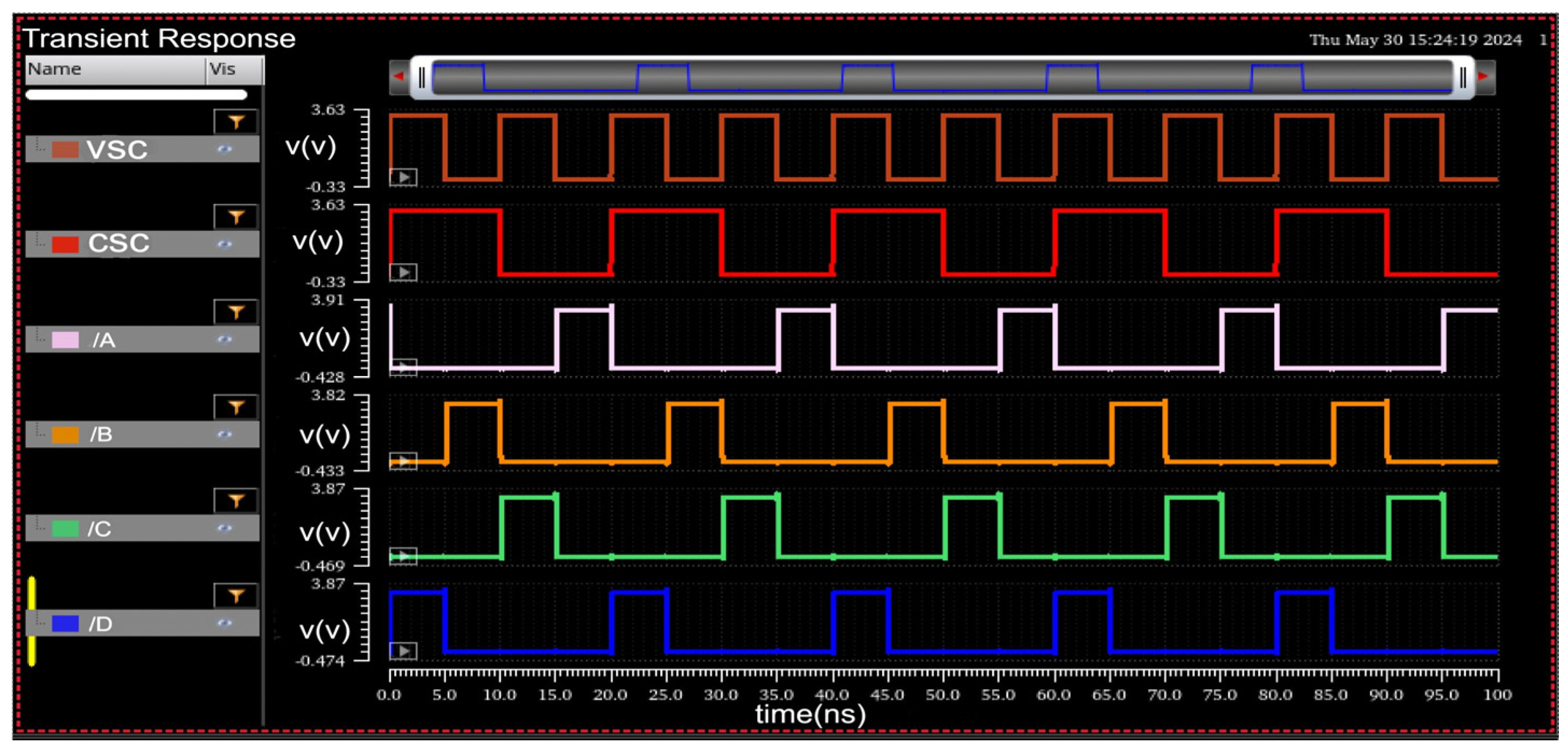
When both amplifiers output a low signal (VSC = 0, CSC = 0), the output gives HIGH for signal A, which is ignored, indicating no fault. If the VSC outputs a low signal and the CSC outputs a high signal (VSC = 0, CSC = 1), the output gives HIGH for signal B, indicating an SC. When the Voltage Sensing Amplifier outputs a HIGH signal, and the Current Sensing Amplifier outputs a low signal (VSC = 1, CSC = 0), the output makes signal C HIGH, signaling an OC condition [36]. Figure 10 provides the simulation results, demonstrating the logic driver circuit’s output for different input combinations.
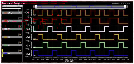
Figure 10.
Logic driver circuit outputs for IN A and IN B: the orange waveform represents an SC in the solar panel, while the green waveform represents an open circuit.
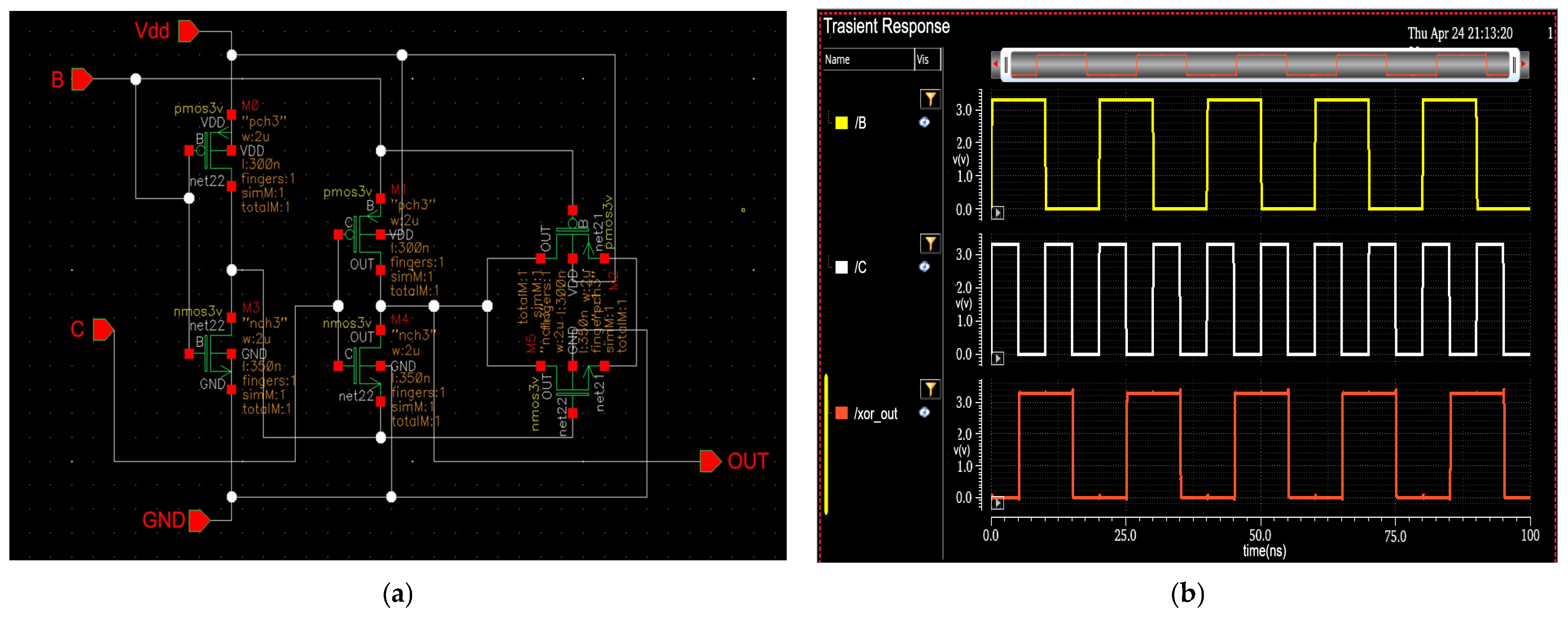
The XOR (exclusive OR) logic gate is a digital circuit that outputs high only when the number of HIGH inputs is odd. The output of an XOR gate is logic 1 if exactly one of its inputs is HIGH [37]. This property makes the XOR gate particularly useful in applications such as error detection, correction, and decision-making circuits. Figure 11b presents the simulation results of the XOR circuit. Specifically, if the outputs corresponding to the OC and SC states (B and C signals) are applied to the XOR gate, it will produce a HIGH output when there is a discrepancy between the two signals [38,39,40]. The last signal in Figure 11b waveforms represents the output of the XOR gate, which is then fed into the next-state memory block. Usually, the XOR gate is designed using a minimum of 12 transistors.

Figure 11.
(a) Six-transistor XOR gate; (b) output blue waveform with a high signal for the 10 and 01 combination.
5.4. Custom Memory Circuit Design
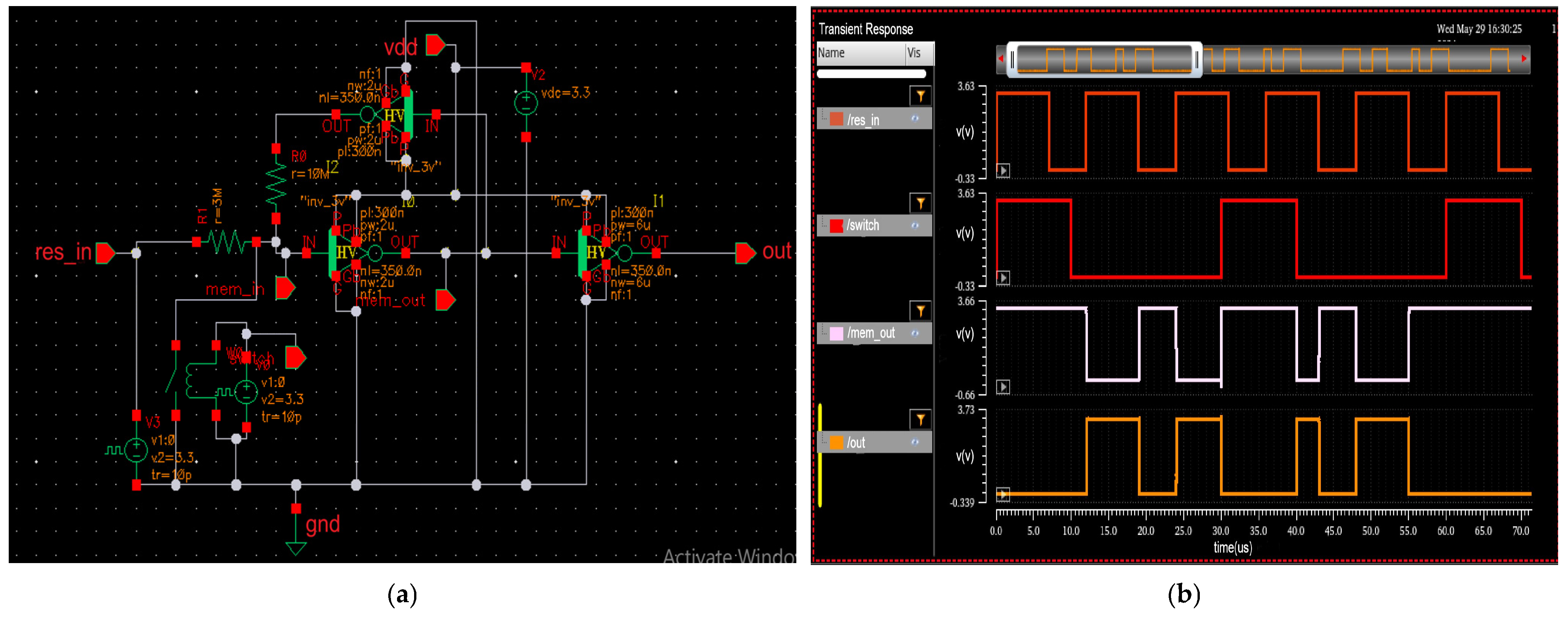
The output from the XOR gate is given to a memory element. This paper presents a memory circuit developed using a back-to-back inverter design, switching between the XOR design’s output and the memory design’s output [41]. This setup functions as a latch or flip-flop, allowing it to store and retain the last output state after the switch is turned on. The XOR gate generates a HIGH 1 output when the system experiences a fault, such as an SC or OC. This HIGH signal is then stored in memory, ensuring the error state is maintained in a back-to-back inverter. As a result, the LED will light up until the error is fixed at the solar panel and rectified by the XOR. The lit LED indicates the error and provides instructions on disconnecting the panel immediately to protect the solar appliances [42].
An external switch is connected to the memory input to reset this stored error signal. Once the SP fault is fixed, the switch can be triggered, resetting the memory and removing the previous error value. This guarantees that the circuit does not continue to signal a fault after fixing the issue [43,44,45,46]. The stored HIGH signal will only be cleared when the reset switch is triggered, making it a reliable mechanism for monitoring SP issues continuously. As we observe the output waveforms from Figure 12b, the first waveform is the input, the second waveform is the switch, and the last waveform is the output [47]. The output waveform is set to LOW 0 whenever the switch is turned on, and the previously stored value is removed. If there is any error at the input when the switch is off, that output is projected at the output and lit by the LED. This helps make sure that short or temporary faults are not missed. It also makes it easier for maintenance teams to find and resolve issues. In this application, the switch used in the memory element is a manual switch. It is intended for user-controlled operation, and used to reset the stored fault signal (SC/OC) after the issue is resolved. This helps make sure that short or temporary faults are not missed. It also makes it easier for maintenance teams to find and resolve issues. This allows us to indicate that home appliances should be disconnected to protect them from short or open circuits.
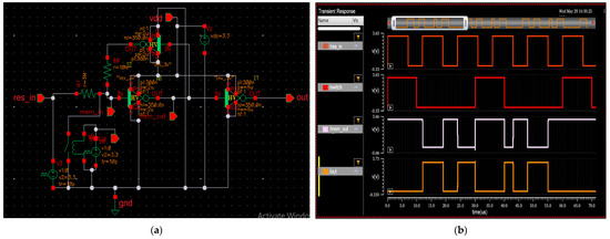
Figure 12.
(a) Memory Circuit with Manual Reset Switch for Fault Signal Storage (b) Input, Reset Switch, and Output Waveforms.
6. ASIC Implementation: Layout and Fabrication
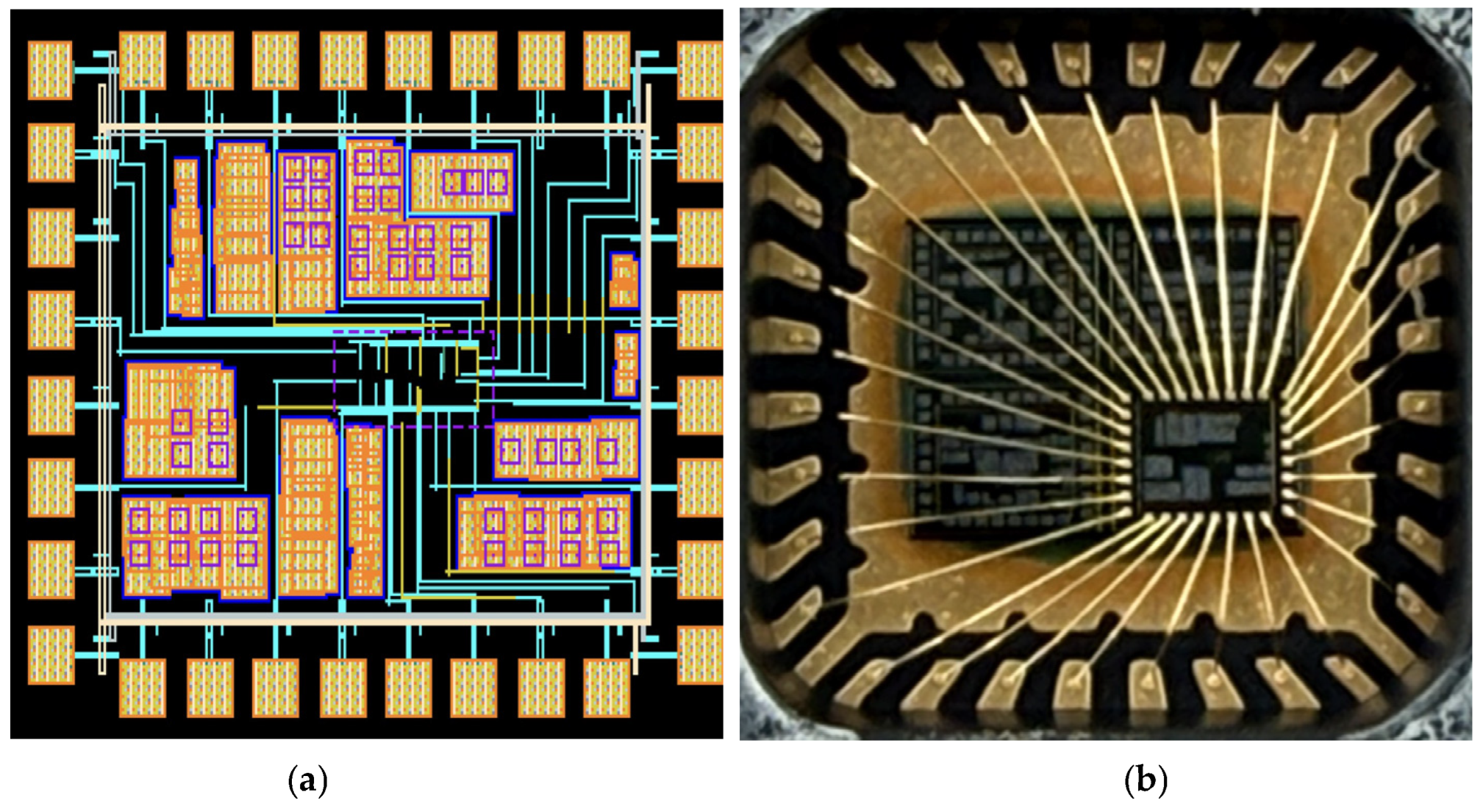
Once all the circuits are implemented and connected into a single integrated circuit, as shown in Figure 5, and the ASIC testing is complete, we can proceed to chip fabrication. We need to convert all the symbolized circuits into the layout form for fabrication. This work has utilized TSMC 180 nm technology and Cadence Virtuoso software for layout design. The TSMC 180 nm technology was selected for ASIC implementation due to its well-established reliability and lower fabrication cost [48]. Compared to advanced nodes (e.g., 7 nm or 28 nm), 180 nm offers greater voltage tolerance, a more straightforward layout for analogue components, and reduced leakage current, essential factors for low-power diagnostic circuits. Additionally, mature process libraries and simplified design rules in 180 nm technology enable faster prototyping and cost-effective production for medium-volume applications such as solar panel diagnostics. A pad was designed to interface with the external world and the chip. Thirty-two pads were placed in a 32-pin pad frame layout. Then, an integrated circuit was placed in the center of the pad frame, connecting each pin to its corresponding pad [49]. We considered the different wire widths for signal and power lines during the connection and applied symmetry techniques for layout designs. We also performed Design Rule Check (DRC) and Layout Versus Schematic (LVS) verification for the entire chip to ensure reliable fabrication. Figure 13a shows the whole chip layout, which was sent for fabrication. The fabricated chip was packaged into a QP-QFN32-5 mm × 5 mm package, as shown in Figure 13b. Since it was a prototype chip, it had 32 pins; however, once all the testing is completed, these 32 can be reduced to 6 pins. The six pins include two for power supply (VDD and GND), two for voltage and current inputs from the solar panel, one for the reference signal input, and one for connecting a manual reset switch to clear the memory after a fault is resolved. This small chip allows for easy mounting directly to the solar panel.

Figure 13.
(a) A 32-pad die with all connections implemented using TSMC 180 nm technology; (b) A QP-QFN32 5 mm × 5 mm package with fabricated chip.
7. Conclusions
This work presents a complete and low-cost diagnostic system for detecting SC and OC faults in SPs. The system was initially implemented on an Intel DE-10 Lite FPGA and later redesigned as a complete ASIC using TSMC 180 nm CMOS technology. Each subsystem was individually developed and validated in FPGA and ASIC domains, including voltage and current sensing, logic drivers, XOR-based fault detection, memory, and clock generation. FPGA-based verification confirmed the functional accuracy of the design using HDL inputs corresponding to SP voltage, current, and clock activation signals. The FPGA output successfully detected SC or OC conditions, as indicated by the LED6 lighting up. For ASIC implementation, differential amplifiers achieving 40 dB gain were used in the VSC and CSC blocks to immediately digitize analog input signals from the SP. A reduced transistor count was achieved using a 12-transistor Logic Driver Circuit (LDC) and a 6-transistor XOR gate. The custom memory block employed a back-to-back inverter latch with a reset switch for fault retention and manual clearing. The final chip layout passed DRC and LVS verification and was packaged using a QP-QFN with a simplified 32-pin interface. In contrast to previous methods relying on machine learning, microcontrollers, or external sensors, often requiring complex computation and additional hardware, the proposed ASIC system performs real-time fault detection entirely with on-chip logic. This makes it highly suitable for low-power PV monitoring, especially for mass production, with costs estimated at under USD 0.50 per unit.
Author Contributions
A.D.: resources, writing—review and editing, validation, software, investigation. S.B.: methodology, project administration, resources, supervision, formal analysis, visualization, software. All authors have read and agreed to the published version of the manuscript.
Funding
This research received no external funding.
Institutional Review Board Statement
Not applicable.
Informed Consent Statement
Not applicable.
Data Availability Statement
The original contributions presented in this study are included in the article.
Conflicts of Interest
The authors declare no conflict of interest.
Abbreviations
The following abbreviations are used in this manuscript:
ASIC | Application-Specific Integrated Circuit |
CMOS | Complementary Metal–Oxide Semiconductor |
CSC | Current-Sensing Circuit |
DA | Differential Amplifier |
FPGA | Field-Programmable Gate Array |
HDL | Hardware Description Language |
IMP | Current at Maximum Power Point |
ISC | Short-Circuit Current |
LDC | Logic Driver Circuit |
OC | Open Circuit |
PMP | Maximum Power Point |
PV | Photovoltaic |
SC | Short Circuit |
SP | Solar Panel |
SPD | Solar Panel Diagnostic |
SQ-L | Shockley–Queisser Limit |
TSMC | Taiwan Semiconductor Manufacturing Company |
VMP | Voltage at Maximum Power Point |
VOC | Open-Circuit Voltage |
VSC | Voltage-Sensing Circuit |
References
- Benestad, R.E.; Schmidt, G.A. Solar trends and global warming. J. Geophys. Res. Atmos. 2009, 114, D14101. [Google Scholar] [CrossRef]
- Jones, A.C.; Hawcroft, M.K.; Haywood, J.M.; Jones, A.; Guo, X.; Moore, J.C. Regional climate impacts of stabilizing global warming at 1.5 K using solar geoengineering. Earth’s Future 2018, 6, 230–251. [Google Scholar] [CrossRef]
- Li, Z.; Yue, J.; Xiang, Y.; Chen, J.; Bian, Y.; Chen, H. Multiresolution analysis of the relationship of solar activity, global temperatures, and global warming. Adv. Meteorol. 2018, 2018, 2078057. [Google Scholar] [CrossRef]
- Al-Ghussain, L. Global warming: Review on driving forces and mitigation. Environ. Prog. Sustain. Energy 2019, 38, 13–21. [Google Scholar] [CrossRef]
- Singh, S.; Kajal, P.; Dhar, A.; Mathews, N.; Boix, P.P.; Powar, S. Reduced global warming potential in carbon-based perovskite solar modules: Cradle-to-gate life cycle analysis. J. Clean. Prod. 2023, 426, 139136. [Google Scholar] [CrossRef]
- Podder, A.K.; Roy, N.K.; Pota, H.R. MPPT methods for solar PV systems: A critical review based on tracking nature. IET Renew. Power Gener. 2019, 13, 1615–1632. [Google Scholar] [CrossRef]
- Ali, A.; Almutairi, K.; Padmanaban, S.; Tirth, V.; Algarni, S.; Irshad, K.; Islam, S.; Zahir, M.H.; Shafiullah, M.; Malik, M.Z. Investigation of MPPT techniques under uniform and non-uniform solar irradiation condition—A retrospection. IEEE Access 2020, 8, 127368–127392. [Google Scholar] [CrossRef]
- Manna, S.; Singh, D.K.; Akella, A.K.; Kotb, H.; AboRas, K.M.; Zawbaa, H.M.; Kamel, S. Design and implementation of a new adaptive MPPT controller for solar PV systems. Energy Rep. 2023, 9, 1818–1829. [Google Scholar] [CrossRef]
- Ahmed, S.T.; Annamalai, A. Improving geo-location performance of lora with adaptive spreading factor. In Proceedings of the 2023 IEEE 13th Symposium on Computer Applications & Industrial Electronics (ISCAIE), Penang Island, Malaysia, 21–22 May 2023. [Google Scholar]
- Sarang, S.A.; Raza, M.A.; Panhwar, M.; Khan, M.; Abbas, G.; Touti, E.; Altamimi, A.; Wijaya, A.A. Maximizing solar power generation through conventional and digital MPPT techniques: A comparative analysis. Sci. Rep. 2024, 14, 8944. [Google Scholar] [CrossRef]
- Solórzano, J.; Egido, M.A. Automatic fault diagnosis in PV systems with distributed MPPT. Energy Convers. Manag. 2013, 76, 925–934. [Google Scholar] [CrossRef]
- García, E.; Ponluisa, N.; Quiles, E.; Zotovic-Stanisic, R.; Gutiérrez, S.C. Solar panels string predictive and parametric fault diagnosis using low-cost sensors. Sensors 2022, 22, 332. [Google Scholar] [CrossRef] [PubMed]
- Hwang, H.-R.; Kim, B.-S.; Cho, T.-H.; Lee, I.-S. Implementation of a fault diagnosis system using neural networks for solar panel. Int. J. Control Autom. Syst. 2019, 17, 1050–1058. [Google Scholar] [CrossRef]
- Garaj, M.; Hong, K.Y.; Chung, H.S.; Zhou, J.; Lo, A.W. Photovoltaic panel health diagnostic system for solar power plants. In Proceedings of the 2019 IEEE Applied Power Electronics Conference and Exposition (APEC), Anaheim, CA, USA, 17–21 March 2019. [Google Scholar]
- Dhanraj, J.A.; Mostafaeipour, A.; Velmurugan, K.; Techato, K.; Chaurasiya, P.K.; Solomon, J.M.; Gopalan, A.; Phoungthong, K. An effective evaluation on fault detection in solar panels. Energies 2021, 14, 7770. [Google Scholar] [CrossRef]
- Selvaraj, T.; Rengaraj, R.; Venkatakrishnan, G.; Soundararajan, S.; Natarajan, K.; Balachandran, P.; David, P.; Selvarajan, S. Environmental fault diagnosis of solar panels using solar thermal images in multiple convolutional neural networks. Int. Trans. Electr. Energy Syst. 2022, 2022, 2872925. [Google Scholar] [CrossRef]
- Bodnár, I.; Kozsely, G. Development of solar panel diagnostic system. In Proceedings of the 2022 23rd International Carpathian Control Conference (ICCC), Sinaia, Romania, 29 May–1 June 2022. [Google Scholar]
- Spataru, S.; Sera, D.; Kerekes, T.; Teodorescu, R. Diagnostic method for photovoltaic systems based on light I–V measurements. Sol. Energy 2015, 119, 29–44. [Google Scholar] [CrossRef]
- Chine, W.; Mellit, A.; Lughi, V.; Malek, A.; Sulligoi, G.; Pavan, A.M. A novel fault diagnosis technique for photovoltaic systems based on artificial neural networks. Renew. Energy 2016, 90, 501–512. [Google Scholar] [CrossRef]
- Available online: https://en.wikipedia.org/wiki/Voltage_divider (accessed on 27 May 2025).
- Kuon, I.; Rose, J. Measuring the gap between FPGAs and ASICs. In Proceedings of the 2006 ACM/SIGDA 14th International Symposium on Field Programmable Gate Arrays, Monterey, CA, USA, 22–24 February 2006. [Google Scholar]
- Hu, Y.; Liu, Y.; Liu, Z. A survey on convolutional neural network accelerators: GPU, FPGA and ASIC. In Proceedings of the 2022 14th International Conference on Computer Research and Development (ICCRD), Shenzhen, China, 7–9 January 2022. [Google Scholar]
- Reddy, B.N.K.; Seetharamulu, B.; Krishna, G.S.; Vani, B.V. An FPGA and ASIC implementation of cubing architecture. Wirel. Pers. Commun. 2022, 125, 3379–3391. [Google Scholar] [CrossRef]
- Boutros, A.; Betz, V. FPGA architecture: Principles and progression. IEEE Circuits Syst. Mag. 2021, 21, 4–29. [Google Scholar] [CrossRef]
- Ahmed, A.A.; Ahmed, S. A real-time car towing management system using ml-powered automatic number plate recognition. Algorithms 2021, 14, 317. [Google Scholar] [CrossRef]
- Wang, T.; Gong, L.; Wang, C.; Yang, Y.; Gao, Y.; Zhou, X.; Chen, H. Via: A novel vision-transformer accelerator based on fpga. IEEE Trans. Comput.-Aided Des. Integr. Circuits Syst. 2022, 41, 4088–4099. [Google Scholar] [CrossRef]
- Vaithianathan, M.; Patil, M.; Ng, S.F.; Udkar, S. Comparative study of FPGA and GPU for high- performance computing and AI. ESP Int. J. Adv. Comput. Technol. (ESP-IJACT) 2023, 1, 37–46. [Google Scholar]
- Machupalli, R.; Hossain, M.; Mandal, M. Review of ASIC accelerators for deep neural network. Microprocess. Microsyst. 2022, 89, 104441. [Google Scholar] [CrossRef]
- Taraate, V. ASIC Design and Synthesis; Springer: Berlin/Heidelberg, Germany, 2021. [Google Scholar]
- Matthus, C.D.; Buhr, S.; KreiBig, M.; Ellinger, F. High gain and high bandwidth fully differential difference amplifier as current sense amplifier. IEEE Trans. Instrum. Meas. 2020, 70, 2000911. [Google Scholar] [CrossRef]
- Ge, Z.; Liu, S.; Li, Z.; Yoshie, O.; Sun, J. Ota: Optimal transport assignment for object detection. In Proceedings of the IEEE/CVF Conference on Computer Vision and Pattern Recognition, Nashville, TN, USA, 20–25 June 2021. [Google Scholar]
- Riaz, A.; Medard, M.; Duffy, K.R.; Yazicigil, R.T. A universal maximum likelihood GRAND decoder in 40nm CMOS. In Proceedings of the 2022 14th International Conference on COMmunication Systems NETworkS (COMSNETS), Bangalore, India, 4–8 January 2022. [Google Scholar]
- Srinivas, C.; Bhargav, G.S.; Chandan, S.P.; Vimala, P. Comparative analysis of decoders using static dynamic CMOS logic. In Proceedings of the 2023 International Conference on Advances in Electronics, Communication, Computing and Intelligent Information Systems (ICAECIS), Bangalore, India, 19–21 April 2023. [Google Scholar]
- Alam, S.; Hutchins, J.; Shukla, N.; Asifuzzaman, K.; Aziz, A. CMOS-based single-cycle in-memory XOR/XNOR. IEEE Access 2024, 12, 49528–49534. [Google Scholar] [CrossRef]
- Kandpal, J.; Tomar, A.; Adhikari, S.; Joshi, V. Design of low power and high speed XOR/XNOR circuit using 90 nm CMOS technology. In Proceedings of the 2019 2nd International Conference on Innovations in Electronics, Signal Processing and Communication (IESC), Shillong, India, 1–2 March 2019. [Google Scholar]
- Binzaid, S.; Divi, A.; Rokonuzzaman, M. Simplifying complex digital sequential circuit by an innovative mixed-signal circuit alternative. Comput. Electr. Eng. 2024, 115, 109126. [Google Scholar] [CrossRef]
- Kim, M.-K.; Kim, I.-J.; Lee, J.-S. CMOS-compatible ferroelectric NAND flash memory for high-density, low-power, and high-speed three-dimensional memory. Sci. Adv. 2021, 7, eabe1341. [Google Scholar] [CrossRef]
- Bobda, C.; Mbongue, J.M.; Chow, P.; Ewais, M.; Tarafdar, N.; Vega, J.C.; Eguro, K.; Koch, D.; Handagala, S.; Leeser, M.; et al. The future of FPGA acceleration in datacenters and the cloud. ACM Trans. Reconfig. Technol. Syst. (TRETS) 2022, 15, 1–42. [Google Scholar] [CrossRef]
- Khursheed, A.; Khare, K. Optimized buffer insertion for efficient interconnects designs. Int. J. Numer. Model. Electron. Netw. Devices Fields 2020, 33, e2748. [Google Scholar] [CrossRef]
- Ndjountche, T. CMOS Analog Integrated Circuits; CRC Press: Boca Raton, FL, USA, 2019. [Google Scholar]
- Dong, M.; Clark, G.; Leenheer, A.J.; Zimmermann, M.; Dominguez, D.; Menssen, A.J.; Heim, D.; Gilbert, G.; Englund, D.; Eichenfield, M. High-speed programmable photonic circuits in a cryogenically compatible, visible–near-infrared 200 mm CMOS architecture. Nat. Photonics 2022, 16, 59–65. [Google Scholar] [CrossRef]
- Rai, P.K.; Srivastava, S.; Johri, A. Design, Layout and Simulation of 8 bit Arithmetic and Logic Circuits Pad frame using C5 Process for deep submicron CMOS. In Proceedings of the 2018 International Conference on Advanced Computation and Telecommunication (ICACAT), Bhopal, India, 28–29 December 2018. [Google Scholar]
- Baker, R.J. CMOS: Circuit Design, Layout, and Simulation; John Wiley & Sons: Hoboken, NJ, USA, 2019. [Google Scholar]
- Wang, C.; Zhang, F.; Lu, F.; Chen, Q.; Li, C.; Wang, A. A study of transient voltage peaking in diode-based ESD protection structures in 28 nm CMOS. IEEE Access 2020, 8, 87164–87172. [Google Scholar] [CrossRef]
- Liu, M.; Zhu, K.; Gu, J.; Shen, L.; Tang, X.; Sun, N.; Pan, D.Z. Towards decrypting the art of analog layout: Placement quality prediction via transfer learning. In Proceedings of the 2020 Design, Automation & Test in Europe Conference & Exhibition (DATE), Grenoble, France, 9–13 March 2020. [Google Scholar]
- Xu, B.; Zhu, K.; Liu, M.; Lin, Y.; Li, S.; Tang, X.; Sun, N.; Pan, D.Z. MAGICAL: Toward fully automated analog IC layout leveraging human and machine intelligence. In Proceedings of the 2019 IEEE/ACM International Conference on Computer-Aided Design (ICCAD), Westminster, CO, USA, 4–7 November 2019. [Google Scholar]
- Quan, H.J.; Jiao, A.Y.; Li, Z.Z.; Chen, Y. Process research of seal ring groove based on magnetic abrasive finishing. Int. J. Manuf. Technol. Manag. 2018, 32, 565–579. [Google Scholar] [CrossRef]
- Dallaev, R.; Pisarenko, T.; Papež, N.; Holcman, V. Overview of the Current State of Flexible Solar Panels and Photovoltaic Materials. Materials 2023, 16, 5839. [Google Scholar] [CrossRef] [PubMed]
- Yuan, J.; Svensson, C. High-speed CMOS circuit technique. IEEE J. Solid-State Circuits 1989, 24, 62–70. [Google Scholar] [CrossRef]
Disclaimer/Publisher’s Note: The statements, opinions and data contained in all publications are solely those of the individual author(s) and contributor(s) and not of MDPI and/or the editor(s). MDPI and/or the editor(s) disclaim responsibility for any injury to people or property resulting from any ideas, methods, instructions or products referred to in the content. |
© 2025 by the authors. Licensee MDPI, Basel, Switzerland. This article is an open access article distributed under the terms and conditions of the Creative Commons Attribution (CC BY) license (https://creativecommons.org/licenses/by/4.0/).