Article

Correlation Between Broken Contact Fingers and I–V Characteristics of Partially Shaded Photovoltaic Modules

1
School of Engineering, Cardiff University, Cardiff CF24 3AA, UK
2
Libyan Fertiliser Company (Lifeco), Marsa El Brega P.O. Box 6796, Libya
3
The Centre for Solar Energy Research and Studies (CSERS), Tripoli P.O. Box 12932, Libya
*
Author to whom correspondence should be addressed.
Solar 2024, 4(4), 595-605; https://doi.org/10.3390/solar4040028
Submission received: 22 July 2024 / Revised: 1 October 2024 / Accepted: 9 October 2024 / Published: 15 October 2024

Abstract

This paper reports on the correlation between broken contact fingers and the shape of the current–voltage (I–V) curve of a photovoltaic (PV) module. It was found that the broken contact fingers of a solar cell in the PV module cause a noticeable change in the I–V curve of the PV module when the solar cell was partially shaded. The broken contact fingers were inspected by microscopic imaging and electroluminescence (EL) imaging, and a further investigation was carried out using a single solar cell. The results show that the fill factor of the cell decreased from 0.75 of full contact to 0.47 after 16 contact fingers were broken, confirming the correlation between the I–V curve shape and broken contact fingers. This result reveals that the shape of the I–V curve of a PV module under individual-cell partial shading may be used as an indicator of broken contact fingers, which offers an alternative approach to EL imaging for detecting broken contact fingers in PV modules in daylight.

1. Introduction

With a long lifetime of about 20 years [1], crystalline silicon (c-Si) photovoltaic (PV) modules dominate the PV market [2]. However, manufacturers of PV modules tend to reduce the wafer thickness in order to reduce the manufacturing cost, which makes solar cells prone to cell breakage and cracks [3,4]. Broken contact fingers of solar cells occur frequently in PV modules. They are usually caused by cracks that cut the contact fingers [5]. Cracks and broken contact fingers may occur during different stages of the module manufacturing, such as the soldering of solar cells [6], lamination [7], transportation and handling [8]. Furthermore, they could develop during operation as a result of temperature cycles, snow and wind loads [9]. Degradation due to installation on a concrete base within high- and low-humidity environments was also assessed [10,11].
In a study performed in [5], the orientation of the cracks produced by mechanical load testing was investigated. The authors found that 50% of the cracks are parallel to the busbars of the cells, which is the orientation of the cracks that cause broken contact fingers [5,12]. In another study reported in [13], the cracks appearing parallel to the busbar represented 21% of the total observed cracks in a PV installation.
Broken contact fingers have a significant impact on the performance of PV modules. Köntges et al. performed a simulation study on power loss due to broken contact fingers in a PV module consisting of 60 solar cells connected in a series [12]. The results revealed that about 20% of the module power output is lost when only one cell has broken contact fingers that disconnect half of its area. Furthermore, it was shown in [12] that the power loss becomes even worse for the cells with a higher breakdown voltage. In an experimental study involving thermal cycling and mechanical load tests on a PV module, Chaturvedi et al. [6] found that the maximum power reduced from 236 W to 228 W due to mechanical loading, and from 241 W to 226 W due to thermal cycling, respectively. Electroluminescence (EL) imaging in [6] revealed that the power reduction was due to broken contact fingers and cracks. In addition, it was confirmed by Dhimish [14] that there is a correlation between broken contact fingers and hot spots. Hot spots in PV modules could damage single solar cells or even the entire PV module [15].
It is therefore imperative to detect the broken contact fingers of PV modules while in operation in the field. Several detection techniques were proposed in the past [16]. They differ in terms of their reliability, applicability, complexity and cost. The most widely used technique is EL imaging, proposed by Fuyuki et al. [17]. The EL inspection of solar cells is based on capturing the infrared (IR) light emitted by solar cells when they are forward-biased [18]. A cooled silicon charge-coupled device (CCD) camera is usually utilized to capture the EL radiation within a dark environment [19]. This technique is easy to implement and has a high accuracy, as shown in [18,20,21]. However, a main disadvantage is its incapability to detect faults in daylight because EL radiation is much weaker than sunlight [22,23]. EL imaging in daylight requires special hardware, filtering techniques and capturing background images with the EL images [23], which is not a straightforward task. Photoluminescence imaging (PL) is another imaging technique that is starting to gain attention for PV module inspection [24,25]. Line-scan PL was proposed in [26], in which light excitation and PL images are performed within thin lines along the width of the solar cell. This technique showed better performance than EL imaging in the detection of broken contact fingers. In addition, it can distinguish between broken contact fingers and recombination defects. However, all thin-line images need to be combined to produce the final complete image of the PV device, which is not a simple process.
The detection of cracks using the I–V curve of PV modules has been recently published [27]. However, this approach, which does not require the shading of individual solar cells, is only effective for detecting severe cracks that can introduce a clear step in the I–V curve of PV modules. As a result, the less severe cracks cannot be detected by this technique. Furthermore, this method cannot identify the specific solar cell in a PV module that has developed cracks. To overcome these limitations, here, we propose incorporating the partial shading of individual cells in the I–V measurements to improve the capability of detecting the health state of contact fingers.
The incorporation of I–V measurement with the partial shading of an individual solar cell is not new, and has been reported for applications such as hot-spot endurance tests [28], hot-spot detection [29,30,31], determining the series resistance [32] and the shunt resistance of individual cells [33,34]. However, to the best of our knowledge, the possibility of using the I–V curve with individual-cell shading for the detection of broken contact fingers in PV modules has not been previously investigated.
This paper experimentally investigates the effect of broken contact fingers on the shape of the I–V curves of PV modules when individual cells are partially shaded. It aimed to provide the proof-of-concept of using partially shaded I–V curves for the detection of broken contact fingers.

2. Experimental Procedure

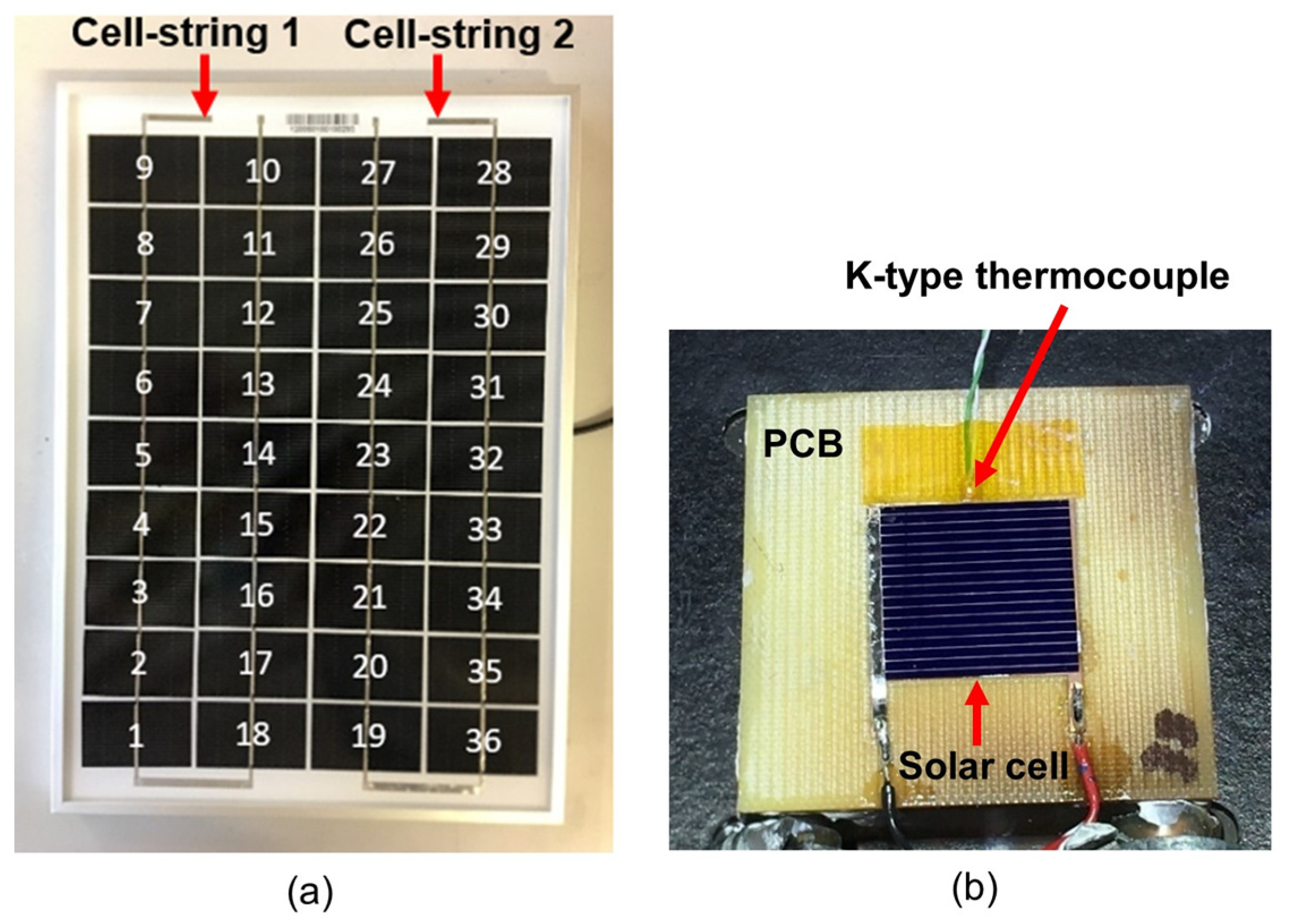
2.1. Preparations of PV Devices

The PV technology employed in this work was mono-crystalline silicon (mono-Si). Two PV devices were prepared for this experimental investigation. Figure 1a shows a 10 W PV module supplied from Betop-camp, which has an area of 34 cm × 24 cm and 36 mono-Si solar cells connected in a series. Bypass diodes were added to the module, with one diode per 18 cells [35]. To facilitate the identification of individual cells, each cell was numbered, as shown in Figure 1a. In order to monitor the temperature of the module during I–V curve measurements, a K-type thermocouple was connected to the back side of the module. The open circuit voltage ( V o c ), short circuit current ( I s c ) and maximum power output ( P max ) of the PV module were measured at a module temperature of 25 °C and an irradiance of 1000 W/m2 at the middle point of the module, which are 23.643 V, 0.516 A and 9.77 W, respectively [35].
The second PV device employed for this study was a single mono-Si solar cell with an active area of 6.25 cm2 (2.5 cm × 2.5 cm), which has a single-edge busbar, as depicted in Figure 1b. The back electrode of the solar cell was soldered on a printed circuit board (PCB), which was mounted on a water heat exchanger [36]. The cell’s temperature was measured during I–V measurements using a K-type thermocouple mounted on the PCB close to the cell, as shown in Figure 1b. This solar cell had a V o c , I s c and P max of 0.6260 V, 0.213 A and 100.4 mW, respectively, under standard test conditions (STCs).

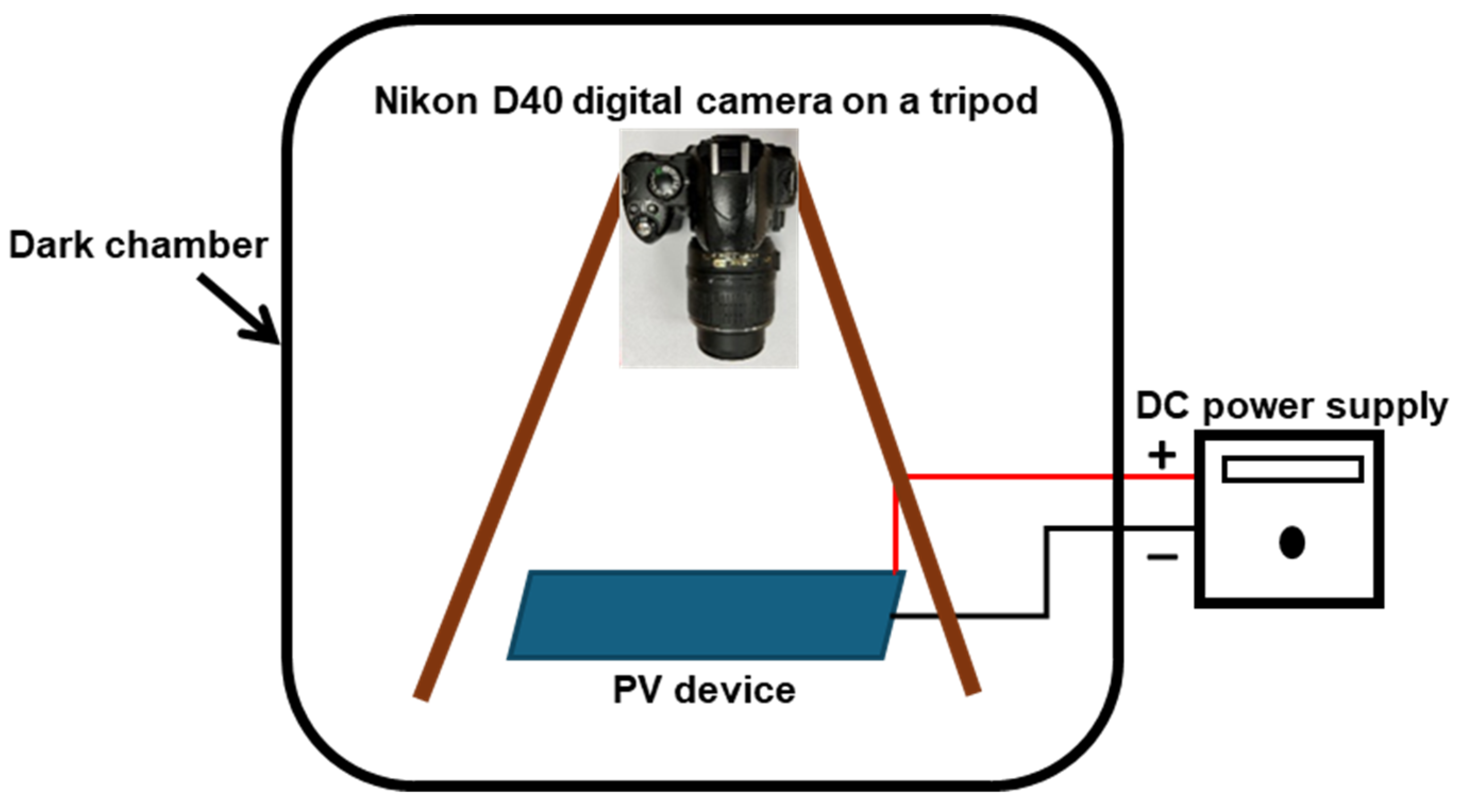
2.2. Setup for I–V Characterization

Figure 2 shows a schematic diagram of the setup for the I–V measurement used in this experiment [35]. The PV devices tested were placed in an environmental chamber that is equipped with a light source (ARRISUN 60) and a test table. The temperature of the PV devices was controlled by a circulating water bath and monitored using a K-type thermocouple and data logger (TC-08) connected to a computer. I–V curve measurements were performed by a Keithley source meter (model 2601) (see ref. [35] for detailed information regarding this test rig).

2.3. EL Imaging Setup

El imaging was used to visualize the broken contact fingers in the PV module and single solar cell. A commercial digital single-lens reflex (DSLR) camera was used in this work with its IR filter removed to allow for the detection of IR radiation [21]. The camera was Nikon D40 with a standard lens that has a focal length of 18–55 mm and a resolution of 3008 × 2000 pixels. The schematic of the EL imaging setup is shown in Figure 3. The PV device under test was put inside the testing chamber in a dark environment. To capture the EL images, the camera was mounted on a tripod with the lens facing down, and the PV device was forward-biased at a current approximately equal to the I s c under STCs [6]. The camera settings were adjusted iteratively until good-quality EL images were captured.

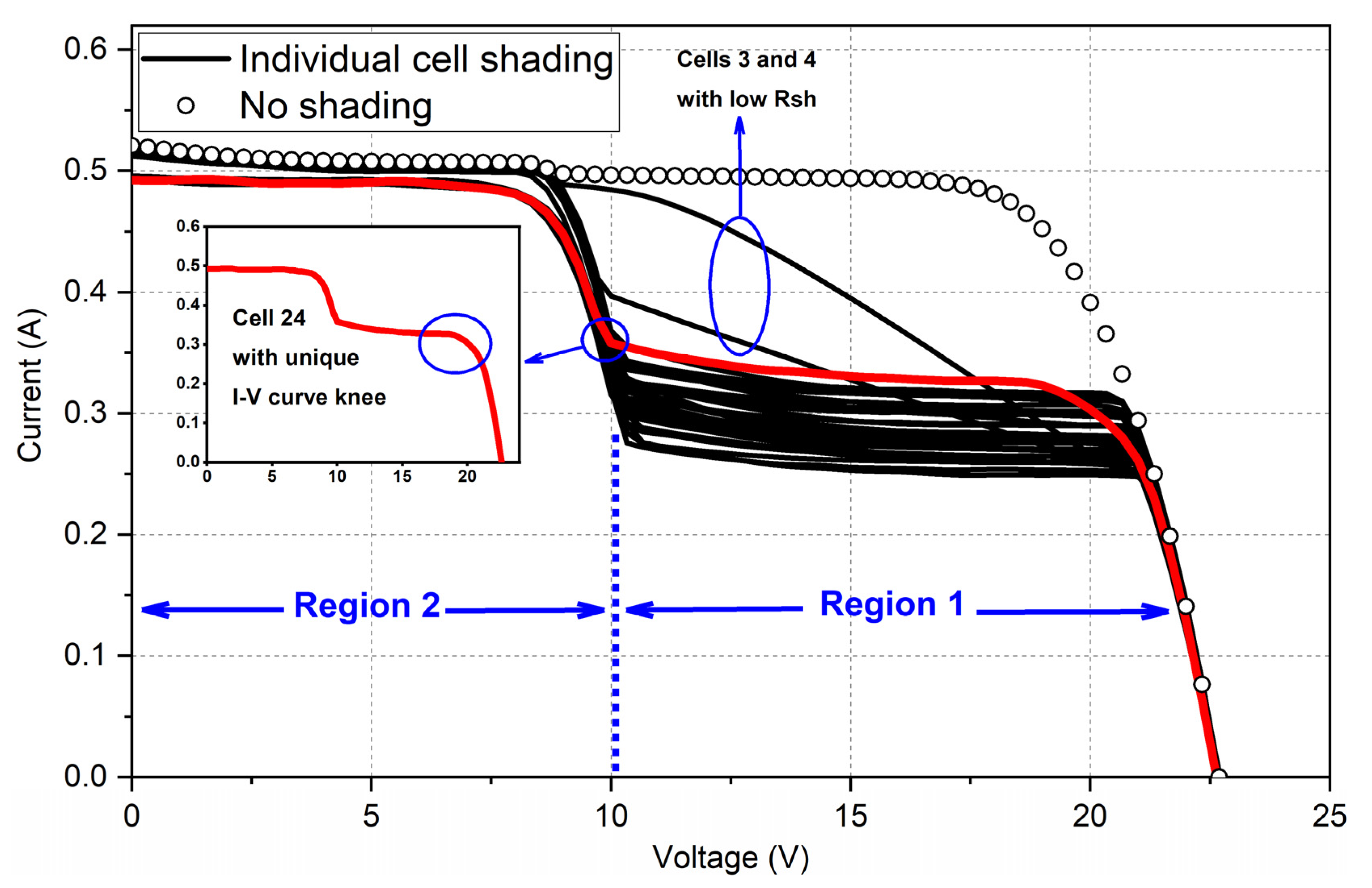
3. I–V Curve Under Individual-Cell Partial Shading

The I–V curves of the PV module shown in Figure 1a were obtained for cases when each cell of the module was subjected to half-shading in turn using an adhesive tape. The measurements were taken at a module temperature of 40 °C and an irradiance of 1000 W/m2 (measured at the middle point of the module). Using the testing system described in Section 2.2, we found that the most stable temperature over a long testing period of >4 h is around 40 °C. Consequently, all tests reported in this work were carried out at a temperature of 40 °C. Figure 4 depicts the I–V curves, together with an I–V curve without shading. The I–V curves under individual-cell shading are clearly divided into two regions, as indicated in the figure due to the conduction of the bypass diodes.
Figure 4 shows the discrepancy among the I–V curves at region 1. The majority of them have an almost identical shape but with a parallel shift along the vertical axis. This can be attributed to the non-uniformity of irradiance incident on the cells, which was found to be 18.9% for an area of 40 cm × 40 cm [35], calculated according to the E927-10 standards [37].
Although a majority of the curves in region 1 exhibited a similar shape, three cells displayed distinctively different shapes. The I–V curves of cells 3 and 4 had higher slopes at region 1, which were due to the low shunt resistance of the cells [33,38,39]. The low shunt resistance caused the current of unshaded cells to flow through the shaded cell in the reverse direction, resulting in a higher slope in region 1. More interestingly, the I–V curve corresponding to cell 24 (solid red line) had a noticeably less sharp knee at the maximum power point (MPP) of region 1. This shape is clearly different from those of the majority of the cells, indicating the unique characteristic of cell 24. The experiment of applying the half-shading of this cell was repeated 12 times over three different days (four measurements each day), and the results confirm that this observation is repeatable (note: only the average of three consecutive I–V measurements obtained in one day is shown here for the sake of clarity).
Cell 24 in the PV module was inspected to identify the cause of the change in its I–V curve. Figure 5a shows an image of the cell captured using a 12-megapixel camera (Nikon D40, Cardiff, UK). A scratch mark, which is perpendicular to the contact fingers, can be seen on the top–right surface of the cell, as indicated by the red circle. In order to examine the damage in detail, the cell was inspected using a microscope (Olympus model SZ, Cardiff, UK) equipped with a 10-megapixel camera (GXCAM-5, GT Vision Ltd., Cardiff, UK). Figure 5b shows the image of a scratch that affected nine contact fingers. A closer image in Figure 5c clearly shows that the contact fingers are broken. A detailed inspection confirms that all nine contact fingers that are affected by the scratch are broken.
The images of cell inspection indicate that the change of the I–V curves of cell 24 is associated with the broken contract fingers. This result provides a possibility to pinpoint the exact cell in a PV module that has broken contact fingers. This can only be achieved by measuring the I–V curves with consecutive partial shading of each single cell in a PV module, as shown in Figure 4. Although the usual I–V measurement of a PV module without shading may reveal the severe damage to the contact fingers, as discussed in [27], less severe damage to the contact fingers cannot be detected from the usual I–V curve without shading, as shown in Figure 4. In addition, the shading test can identify the specific cell that has broken contact fingers. Clearly, the discovery presented in Figure 4 offers a viable method to provide information on the health of individual cells in a PV module, particularly associated with broken contact fingers. It is to be noted that the results of I–V tests can also be presented as the J–V curves of the PV panels. The advantage of using J–V curves needs to be further investigated.
To provide further evidence, the PV module used to obtain Figure 4 was inspected by EL imaging using the setup described in Section 2.3. Figure 6 shows the EL image of the PV module. A dark region can be seen clearly in the top–right corner of cell 24, which coincides precisely with the position of the damaged contact fingers, as shown in Figure 5a. Without the presence of a sufficient electrical current due to broken contact fingers, the EL image of this part becomes much darker. This provides strong evidence to confirm the cause of the shape change in the partially shaded I–V curves observed in Figure 4 (i.e., due to the broken contact fingers).

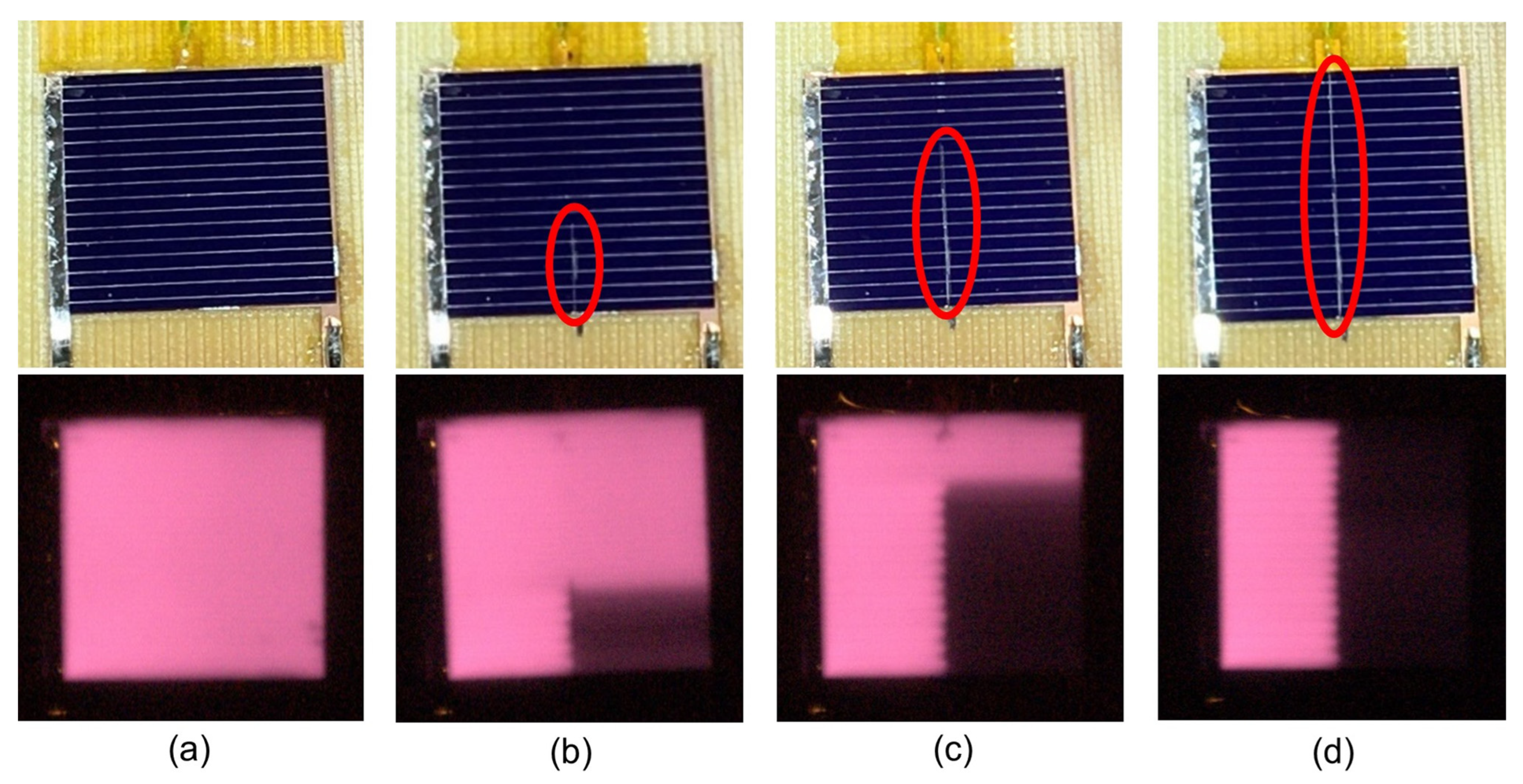
4. Influence of Broken Contact Fingers on a Single Solar Cell

The correlation between the change of shaded I–V curves and broken contact fingers, observed in cell 24 of the PV module was further investigated using a solar cell with intentional damage to its contact fingers. The solar cell shown in Figure 1b was employed for this study, which had 16 contact fingers. Before damage, the solar cell was inspected by EL imaging using the same setup described in Section 2.3. The measured EL image is shown in Figure 7a and the corresponding I–V curve is shown by the black solid line in Figure 8a. The EL image shows no dark region because the electrical current is uniformly distributed over the whole surface due to satisfactory electrical contacts. The intentional damage was carried out by scratching the cell surface along a direction perpendicular to contact fingers. Initially, six contact fingers were intentionally broken from the center–bottom of the cell. Then, its EL image was captured, as shown in Figure 7b. A dark region clearly appeared that coincides with the area where the contact fingers were damaged. This was accompanied by a shape change in its corresponding I–V curve, as shown by the red dashed line in Figure 8a. This process was repeated by breaking the next 5 contact fingers (a total of 11 contact fingers damaged), and then the last 5 contact fingers (a total of 16 contact fingers damaged). The corresponding EL images are shown in Figure 7c,d, and the I–V curves are shown by the blue and green dashed lines in Figure 8a, respectively. The I–V curves are the average of 12 measurements obtained over three days with four measurements each day to ensure reproducibility. The error bars represent the standard deviation of the measured current at given voltage points. The change in the fill factor (FF) corresponding to the I–V curve measurements is shown in Figure 8b.
The results of Figure 7 and Figure 8 confirm the correlation between the shape change in I–V curves and damaged contact fingers. The curvature of the I–V curves at MPP in Figure 8a becomes gradually less sharp with an increasing number of broken contact fingers. This is clearly correlated to the increasing size of the dark part of EL images shown in Figure 7b–c, which indicates poorer electrical contact due to damage. As a result, the FF of the solar cell is reduced, as shown in Figure 8b. These results provide supporting evidence, confirming that the shape change of the partially shaded I–V curve in Figure 4 was caused by a decrease in the FF of cell 24 as a result of damaged contact fingers. It is to be noted that the short-circuit current I s c is not significantly affected by the number of damaged contact fingers, as shown in Figure 8a. However, the load current corresponding to the maximum power output is significantly reduced.

5. Conclusions

This study discovered a correlation between broken contact fingers and the shape of I–V curves under individual-cell partial shading, offering a possibility for the detection of solar cell broken contact fingers which cannot be detected from usual I–V measurements without shading. It was observed that one of the I–V curves resulting from individual-cell shading exhibited a reduced curvature at the MPP of region 1. This behavior has been investigated using microscopic imaging and EL imaging, and it was found to be correlated to the broken contact fingers of the cell. Further investigation carried out on a single solar cell shows that the FF decreases with an increasing number of broken contact fingers, which explains the shape of the I–V curve observed in cell 24 when it was partially shaded.
The study shows that the I–V curves of a PV module under individual-cell partial shading can identify the specific solar cell in a PV module that has broken contact fingers. This offers a possibility to develop a new method for the detection of broken contact fingers using partial-shading I–V measurements in daylight. It is to be noted that the change in the I–V curve can be caused by other defects (such as an increase in series resistance) and is not only associated with broken contact fingers.

Author Contributions

Conceptualization, A.A.; Data curation, A.A.; Formal analysis, A.A., F.A. and G.M.; Funding acquisition, A.A., A.B. and G.M.; Investigation, A.A., A.B. and G.M.; Methodology, A.A., F.A. and G.M.; Project administration, F.A. and G.M.; Resources, G.M.; Supervision, F.A. and G.M.; Validation, A.A.; Visualization, A.A.; Writing—original draft, A.A.; Writing—review and editing, A.A., F.A., A.B. and G.M. All authors have read and agreed to the published version of the manuscript.

Funding

The Ministry of Education of Libya sponsored the Ph.D. project of A.A.; EPSRC (EP/K022156/1) for facilities.

Institutional Review Board Statement

Not applicable.

Informed Consent Statement

Not applicable.

Data Availability Statement

Data will be made available at the Cardiff University Data Repository.

Acknowledgments

The authors would like to thank the Mechanical and Electrical Workshops at Cardiff University for providing the heat exchangers and PCB. The authors also acknowledge EPSRC for the solar cell characterization facility. Abdulhamid Atia expresses his thanks to the Ministry of Education of Libya for his PhD scholarship. EPSRC is acknowledged for the use of solar cell characterization facilities developed under projects EP/K029142/1 and EPK022156/1.

Conflicts of Interest

The authors declare no conflicts of interest. Abdulhamid Atia is also affiliated with the Libyan Fertiliser Company and declares no conflicts of interest.

References

  1. Mertens, K. Photovoltaics Fundamentals, Technology and Practice; Wiley: Chichester, UK, 2014. [Google Scholar]
  2. Masson, G.; Kaizuka, I. Trends in Photovoltaic Applications 2022. Available online: https://iea-pvps.org/trends_reports/trends-2022/ (accessed on 7 October 2024).
  3. Wang, P.A. Industrial challenges for Thin Wafer Manufacturing. In Proceedings of theIEEE 4th World Conference on Photovoltaic Energy Conversion, WCPEC-4, IEEE Computer Society, Waikoloa, HI, USA, 7–12 May 2006; IEEE: New York, NY, USA; pp. 1179–1182. [Google Scholar] [CrossRef]
  4. Papargyri, L.; Theristis, M.; Kubicek, B.; Krametz, T.; Mayr, C.; Papanastasiou, P.; Georghiou, G.E. Modelling and experimental investigations of microcracks in crystalline silicon photovoltaics: A review. Renew. Energy 2020, 145, 2387–2408. [Google Scholar] [CrossRef]
  5. Kajari-Schröder, S.; Kunze, I.; Eitner, U.; Köntges, M. Spatial and orientational distribution of cracks in crystalline photovoltaic modules generated by mechanical load tests. Sol. Energy Mater. Sol. Cells 2011, 95, 3054–3059. [Google Scholar] [CrossRef]
  6. Chaturvedi, P.; Hoex, B.; Walsh, T.M. Broken metal fingers in silicon wafer solar cells and PV modules. Sol. Energy Mater. Sol. Cells 2013, 108, 78–81. [Google Scholar] [CrossRef]
  7. Tippabhotla, S.K.; Radchenko, I.; Song, W.J.R.; Illya, G.; Handara, V.; Kunz, M.; Tamura, N.; Tay, A.A.O.; Budiman, A.S. From cells to laminate: Probing and modeling residual stress evolution in thin silicon photovoltaic modules using synchrotron X-ray micro-diffraction experiments and finite element simulations. Prog. Photovolt. Res. Appl. 2017, 25, 791–809. [Google Scholar] [CrossRef]
  8. Köntges, M.; Siebert, M.; Morlier, A.; Illing, R.; Bessing, N.; Wegert, F. Impact of transportation on silicon wafer-based photovoltaic modules. Prog. Photovolt. Res. Appl. 2016, 24, 1085–1095. [Google Scholar] [CrossRef]
  9. Köntges, M.; Kajari-Schröder, S.; Kunze, I. Crack statistic for wafer-based silicon solar cell modules in the field measured by UV fluorescence. IEEE J. Photovolt. 2013, 3, 95–101. [Google Scholar] [CrossRef]
  10. Khan, F.; Alshahrani, T.; Fareed, I.; Kim, J.H. A comprehensive degradation assessment of the silicon photovoltaic modules installed on concrete base under hot and low-humidity environments: Building applications. Sustain. Energy Technol. Assess. 2022, 52, 102314. Available online: https://www.sciencedirect.com/science/article/pii/S2213138822003666 (accessed on 7 October 2024). [CrossRef]
  11. Khan, F.; Rezgui, B.D.; Kim, J.H. Reliability study of c-Si PV module mounted on a concrete slab by thermal cycling using electroluminescence scanning: Application in future solar roadway. Materials 2020, 13, 470. [Google Scholar] [CrossRef]
  12. Köntges, M.; Kunze, I.; Kajari-Schröder, S.; Breitenmoser, X.; Bjørneklett, B. The risk of power loss in crystalline silicon based photovoltaic modules due to micro-cracks. Sol. Energy Mater. Sol. Cells 2011, 95, 1131–1137. [Google Scholar] [CrossRef]
  13. Morlier, A.; Haase, F.; Köntges, M. Impact of cracks in multicrystalline silicon solar cells on PV module power—A simulation study based on field data. IEEE J. Photovolt. 2015, 5, 1735–1741. [Google Scholar] [CrossRef]
  14. Dhimish, M. Micro cracks distribution and power degradation of polycrystalline solar cells wafer: Observations constructed from the analysis of 4000 samples. Renew. Energy 2020, 145, 466–477. [Google Scholar] [CrossRef]
  15. Dhimish, M.; Holmes, V.; Mather, P.; Sibley, M. Novel hot spot mitigation technique to enhance photovoltaic solar panels output power performance. Sol. Energy Mater. Sol. Cells 2018, 179, 72–79. [Google Scholar] [CrossRef]
  16. Abdelhamid, M.; Singh, R.; Omar, M. Review of microcrack detection techniques for silicon solar cells. IEEE J. Photovolt. 2014, 4, 514–524. [Google Scholar] [CrossRef]
  17. Fuyuki, T.; Kondo, H.; Yamazaki, T.; Takahashi, Y.; Uraoka, Y. Photographic surveying of minority carrier diffusion length in polycrystalline silicon solar cells by electroluminescence. Appl. Phys. Lett. 2005, 86, 262108. [Google Scholar] [CrossRef]
  18. Muehleisen, W.; Eder, G.C.; Voronko, Y.; Spielberger, M.; Sonnleitner, H.; Knoebl, K.; Ebner, R.; Ujvari, G.; Hirschl, C. Outdoor detection and visualization of hailstorm damages of photovoltaic plants. Renew. Energy 2018, 118, 138–145. [Google Scholar] [CrossRef]
  19. Fuyuki, T.; Kitiyanan, A. Photographic diagnosis of crystalline silicon solar cells utilizing electroluminescence. Appl. Phys. A Mater. Sci. Process. 2009, 96, 189–196. [Google Scholar] [CrossRef]
  20. Dhimish, M.; Holmes, V.; Mehrdadi, B.; Dales, M. The impact of cracks on photovoltaic power performance. J. Sci. Adv. Mater. Devices 2017, 2, 199–209. [Google Scholar] [CrossRef]
  21. Frazão, M.; Silva, J.A.; Lobato, K.; Serra, J.M. Electroluminescence of silicon solar cells using a consumer grade digital camera. Measurement 2017, 99, 7–12. [Google Scholar] [CrossRef]
  22. Stoicescu, L.; Reuter, M.; Werner, J.H. DaySy: Luminescence imaging of PV modules in daylight. In Proceedings of the 29th European Photovoltaic Solar Energy Conference and Exhibition, Amsterdam, The Netherlands, 23–25 September 2014; pp. 2553–2554. [Google Scholar]
  23. Alves Dos Reis Benatto, G.; Mantel, C.; Spataru, S.; Santamaria Lancia, A.A.; Riedel, N.; Thorsteinsson, S.; Poulsen, P.B.; Parikh, H.; Forchhammer, S.; Sera, D. Drone-based daylight electroluminescence imaging of PV modules. IEEE J. Photovolt. 2020, 10, 872–877. [Google Scholar] [CrossRef]
  24. Trupke, T.; Bardos, R.A.; Schubert, M.C.; Warta, W. Photoluminescence imaging of silicon wafers. Appl. Phys. Lett. 2006, 89, 044107. [Google Scholar] [CrossRef]
  25. Bhoopathy, R.; Kunz, O.; Juhl, M.; Trupke, T.; Hameiri, Z. Outdoor photoluminescence imaging of photovoltaic modules with sunlight excitation. Prog. Photovolt. Res. Appl. 2018, 26, 69–73. [Google Scholar] [CrossRef]
  26. Zafirovska, I.; Juhl, M.K.; Weber, J.W.; Wong, J.; Trupke, T. Detection of finger interruptions in silicon solar cells using line scan photoluminescence imaging. IEEE J. Photovolt. 2017, 7, 1496–1502. [Google Scholar] [CrossRef]
  27. Ma, M.; Zhang, Z.; Yun, P.; Xie, Z.; Wang, H.; Ma, W. Photovoltaic module current mismatch fault diagnosis based on I-V data. IEEE J. Photovolt. 2021, 11, 779–788. [Google Scholar] [CrossRef]
  28. CEI/IEC 61215; Crystalline Silicon Terrestrial Photovoltaic (PV) Modules—Design Qualification and Type Approval. IEC: Geneva, Switzerland, 2005. Available online: https://solargostaran.com/files/standards/IEC/IEC%2061215-2005.pdf (accessed on 7 October 2024).
  29. Herrmann, W.; Wiesner, W.; Vaassen, W. Hot spot investigations on PV modules—New concepts for a test standard and consequences for module design with respect to bypass diodes. In Conference Record of the Twenty Sixth IEEE Photovoltaic Specialists Conference, Anaheim, CA, USA, 29 Septemebr–3 October 1997; IEEE: Anaheim, CA, USA, 1997; pp. 1129–1132. [Google Scholar] [CrossRef]
  30. Wang, Y.; Itako, K.; Kudoh, T.; Koh, K.; Ge, Q. Voltage-based hot-spot detection method for photovoltaic string using a projector. Energies 2017, 10, 230. [Google Scholar] [CrossRef]
  31. Yang, S.; Itako, K.; Kudoh, T.; Koh, K.; Ge, Q. Monitoring and suppression of the typical hot-spot phenomenon resulting from low-resistance defects in a PV string. IEEE J. Photovolt. 2018, 8, 1809–1817. [Google Scholar] [CrossRef]
  32. Kim, Y.S.; Kang, S.M.; Johnston, B.; Winston, R. A novel method to extract the series resistances of individual cells in a photovoltaic module. Sol. Energy Mater. Sol. Cells 2013, 115, 21–28. [Google Scholar] [CrossRef]
  33. d’Alessandro, V.; Guerriero, P.; Daliento, S.; Gargiulo, M. A straightforward method to extract the shunt resistance of photovoltaic cells from current-voltage characteristics of mounted arrays. Solid State Electron. 2011, 63, 130–136. [Google Scholar] [CrossRef]
  34. Alers, G.B.; Zhou, J.; Deline, C.; Hacke, P.; Kurtz, S.R. Degradation of individual cells in a module measured with differential IV analysis. Prog. Photovolt. Res. Appl. 2011, 19, 977–982. [Google Scholar] [CrossRef]
  35. Atia, A.; Anayi, F.; Gao, M. Influence of shading on solar cell parameters and modelling accuracy improvement of PV modules with reverse biased solar cells. Energies 2022, 15, 9067. [Google Scholar] [CrossRef]
  36. Al-Shidhani, M.; Al-Najideen, M.; Rocha, V.G.; Min, G. Design and testing of 3D printed cross compound parabolic concentrators for LCPV system. In Proceedings of the 14th International Conference on Concentrator Photovoltaic Systems (CPV-14), Puertollano, Spain, 16–18 April 2018; American Institute of Physics Inc.: College Park, MD, USA, 2018; p. 020001. [Google Scholar] [CrossRef]
  37. E0927-10; Standard Specification for Solar Simulation for Terrestrial Photovoltaic Testing. ASTM: West Conshohocken, PA, USA, 2010. Available online: https://www.astm.org/e0927-10.html (accessed on 7 October 2024).
  38. Meyer, E.L.; Van Dyk, E.E. The effect of reduced shunt resistance and shading on photovoltaic module performance. In Conference Record of the Thirty-First IEEE Photovoltaic Specialists Conference, Lake Buena Vista, FL, USA, 3–7 January 2005; IEEE: Lake Buena Vista, FL, USA, 2005; pp. 1331–1334. [Google Scholar] [CrossRef]
  39. Daliento, S.; Di Napoli, F.; Guerriero, P.; d’Alessandro, V. A modified bypass circuit for improved hot spot reliability of solar panels subject to partial shading. Sol. Energy 2016, 134, 211–218. [Google Scholar] [CrossRef]
Figure 1. Photographs of the PV devices used in this investigation: (a) 10 W PV module; (b) single solar cell mounted on the PCB with a K-type thermocouple close to it.
Solar 04 00028 g001
Figure 2. Schematic diagram of the setup for I–V curve measurement.
Solar 04 00028 g002
Figure 3. Schematic diagram of the setup for EL imaging.
Solar 04 00028 g003
Figure 4. I–V curves of the 10 W PV module obtained experimentally with half-shading on each individual cell. The I–V curves were measured at a module temperature of 40 °C and an irradiance of 1000 W/m2 at the middle point of the module. Each I–V curve shown is the average of three consecutive measurements. The I–V curve without shading is also included for comparison.
Solar 04 00028 g004
Figure 5. Images of the cell surface show the damage to the contact fingers of cell 24 in the 10 W PV module: (a) photograph of cell 24 taken by a 12-megapixel camera, which has a total cell area of 15 cm2 (3 cm × 5 cm); (b) a microscopic image shows a scratch mark affecting nine contact fingers; (c) a microscopic image shows the breakage of the contact fingers.
Solar 04 00028 g005
Figure 6. EL image of the 10 W PV module shows that cell 24 has a dark region due to broken contact fingers.
Solar 04 00028 g006
Figure 7. Normal images (top) and EL images (bottom) of a single solar cell showing four cases of broken contact fingers: (a) no broken contact fingers; (b) 6 broken contact fingers; (c) 11 broken contact fingers; (d) 16 broken contact fingers.
Solar 04 00028 g007
Figure 8. The effect of broken contact fingers on (a) the I–V curve; (b) fill factor of the solar cell. The I–V curves were measured at a cell temperature of 25 °C and an irradiance of 1000 W/m2. Each I–V curve shown is the average of 12 measurements obtained over three days, with four consecutive measurements each day.
Solar 04 00028 g008
Disclaimer/Publisher’s Note: The statements, opinions and data contained in all publications are solely those of the individual author(s) and contributor(s) and not of MDPI and/or the editor(s). MDPI and/or the editor(s) disclaim responsibility for any injury to people or property resulting from any ideas, methods, instructions or products referred to in the content.

