Article

An Atmospheric Turbulence Compensation Algorithm Based on FSM-DM Cascaded AO Architecture for FSO Communications

1
College of Information Science and Electronic Engineering, Zhejiang University, 38 Zheda Road, Xihu District, Hangzhou 310027, China
2
College of Aerospace, Harbin Institute of Technology, 92 West Dazhi Street, Nangang District, Harbin 150001, China
3
5G Innovation Centre (5GIC), University of Surrey, Guildford GU2 7XH, UK
4
Peng Cheng Laboratory, No. 2, Xingke 1st Street, Nanshan District, Shenzhen 518000, China
*
Authors to whom correspondence should be addressed.
Network 2022, 2(2), 270-287; https://doi.org/10.3390/network2020018
Submission received: 27 February 2022 / Revised: 24 April 2022 / Accepted: 28 April 2022 / Published: 5 May 2022

Abstract

:
Free-space optics (FSO) communication enjoys desirable modulation rates at unexploited frequency bands, however, its application is hindered by atmospheric turbulence which causes phase shifting in laser links. Although a single deformable mirror (DM) adaptive optics (AO) system is a good solution, its performance remains unsatisfactory as the proportion of tilts aberrations becomes relatively high. This condition happens when the incident angle of the laser beam for the optical receiver dynamically shifts. To tackle this problem, we introduce a fast steering mirror (FSM), DM cascaded AO architecture, based upon which we also propose an atmospheric turbulence compensation algorithm. In this paper, we compare the compensation ability of FSM and DM towards tilts aberrations. Furthermore, we gain model matrices for FSM and DM from testbed and simulatively verify the effectiveness of our work. For a Kolmogorov theory-based atmospheric turbulence disturbed incident laser beam where the tilt components take up 80 % of the total proportion of wavefront aberrations, our proposed architecture compensates the input wavefront to a residual wavefront root mean square (RMS) of 1 16 wavelength, compared to 1 6 wavelength for single DM architecture. The study intends to overcome atmospheric turbulence and has the potential to guide the development of future FSO communications.

1. Introduction

The explosive proliferation of wireless communications poses a shortage of frequency band resources [1]. FSO communications have been increasingly attractive due to the large capacity brought by unexploited spectrum as well as high security [2]. Nevertheless, despite their promising prospects, atmospheric turbulence has long been the principal encumbrance clogging the development of the subject. Spatially, inhomogeneities of temperature, humidity, momentum and other atmospheric components lead to a space-varying atmospheric refractive index along the transmission link causing phase shifting. Meanwhile, the existence of atmosphere turbulence significantly enhances the vertical and horizontal exchange of the above atmospheric components which is greater than the exchange intensity of molecular motion. Such influence is generalized as atmospheric turbulence. Displayed in the dynamic variation of the amplitude and phase of the received laser signal, the influence gradually becomes prominent when distance between communication terminals goes beyond 1 km [3]. According to [4], various models of the power spectrum were established to describe statistical features including the Kolmogorov power-law spectrum, the Tatarskii spectrum, the von Karman spectrum, and the modified atmospheric spectrum.
In this study, we focus on a ground-to-ground scenario where communications happen between base stations. The study conducts theoretical pre-research for the subsequent use of laser communication base stations instead of microwave relay base stations so as to achieve 40∼100 Gbps communication rate. As a basic method to improve signal-to-noise ratio (SNR) at the receiver so as to enhance service quality, enlarging SNR from the sender would be an effective method but it is not always the most agreeable solution. On the contrary, correcting phase shifting, compensating wavefront aberrations would benefit the sender in terms of energy saving. Therefore, AO aiming at extracting real-time wavefront distortion and dynamically compensating wavefront aberrations rises up as a prospective countermeasure which could reduce the likelihood of signal fading and mitigate intensity variations (scintillation) [5,6]. Existing studies [7,8,9] have shown that AO techniques are of significant practical value in satellite-to-ground optical communication. Our findings are not only applicable to ground-to-ground FSO communications; as long as it involves dynamically compensating the incident light with a continuously changing phase, our algorithm can be effective with wavefront correctors with suitable stroke. For example, in optical modulation, beam shaping, astronomy, and microscopic imaging [10,11,12].
In general, an AO system consists of a wavefront reconstructor, a wavefront sensor, and a wavefront corrector [13], where the wavefront sensor generates real-time feedback of wavefront aberrations and the wavefront reconstructor computes commands instructing an appropriate deformation of the corrector. The Shark-Hartmann wavefront sensor (SHWS) which gauges atmospherically induced wavefront aberrations across an aperture is widely used in diverse studies [14,15,16,17]. In addition, embedded development boards free from the operating system with better instantaneity and a flexible size would be better suited for a wavefront reconstructor than computers in engineering applications. As for the wavefront corrector, DMs are the most frequently employed optical hardware, among which, micromachined membrane DMs (MMDM) [18] taking advantage of low hysteresis and negligible power consumption are applicable in high-precision scenarios. By contrast, piezoelectric DMs (PDM) [19] benefit from large strokes and high response frequency, satisfying the demand of large-scale aberration compensation. Apart from the above two DMs, unimorph DMs [20] and liquid DMs [21] are indispensable devices used in many AO architectures as well. In addition to DMs, some studies [22] also introduce a tip-tilt mirror into the system to compensate for tilt aberration.
For double wavefront correctors’ AO architecture, the distribution scheme of the workload determines the performance of an algorithm. Additionally, the modeling strategy affects the implementation of modeling and the computation of controlling voltages. Refs. [23,24] used a Lagrange-multiplier (LM)-based damped least-squares (DLS) control method based on a function of wavefront slopes for controlling voltages. It solved controlling voltages by multiplying the inverse of the influence matrix to the left of the sensed wavefont slopes. The method receives effective results, though, it cannot thoroughly remove the coupling between wavefront correctors. Therefore, the damping factor should be designed carefully. Otherwise, either a conservative iteration step is selected or the stability of the algorithm may suffer a loss. In [25,26], the authors decouple low-order aberrations from high-order aberrations by separating Zernike coefficients and distributing a reasonable workload to wavefront correctors. However, the modeling strategy for FSM considers angle value as a variable of Zernike coefficients. Similarly, the model for DM depicts the influence of controlling voltages towards Zernike coefficients. Firstly, the Zernike coefficients cannot be directly observed from SHWS which may introduce a fitting error into the model by using a wavefront restoration matrix fitting Zernike coefficients from wavefront slopes. Secondly, controlling voltages are the direct signal when using an embedded development board which means that another mapping relationship can be built when controlling FSM. To make the dependent and independent variables in a modeling strategy more intuitive, refs. [27,28] built a linear mapping relationship between controlling voltages and wavefront slopes and used a digital PI controller when solving controlling voltages. The latter arranges the Zernike polynomials into a matrix and makes a linear transformation to make the algorithm adapt to irregular pupil regions. Nevertheless, according to our previous work [29], the spots offsets (which are proportional to the wavefront slopes) are a linear function of the square of the controlling voltages. Consequently, we separate the Zernike coefficients to distribute the workload considering the balance of complexity and performance and use a complete second-order modeling strategy to depict the mapping relationship between spots offsets and controlling voltages. Furthermore, due to the nonlinearity of the model structure, we use an iterative method to solve controlling voltages.
The main contribution of this paper is that we use Zernike mode decomposition to decompose the wavefront into 2nd, 3rd and 4th∼15th orders, and use FSM to compensate for low-order aberrations with DM compensating for high-order aberrations, which improves the compensation range and response rate to tilts aberrations of the AO architecture allowing the AO architecture to high-dynamically compensate aberrations. Then, the DM is modeled with the complete second-order model and the FSM is modeled with the coupled second-order model to ensure compensation accuracy. Finally, we use the iterative compensation algorithm to solve the controlling voltages.
The remainder of this paper is structed as follows: Section 2 introduces the proposed FSM-DM cascaded architecture. Section 3 introduces our proposed high-dynamic atmospheric turbulence compensation algorithm which is our main contribution. Section 4 illustrates experimental simulative results collected from our testbed which is our third contribution. Finally, conclusions are drawn in Section 5.

2. FSM-DM Cascaded AO Architecture

In this section, we demonstrate the design of our proposed AO architecture and compare the theoretical potential of DM and FSM compensating tilts aberrations.

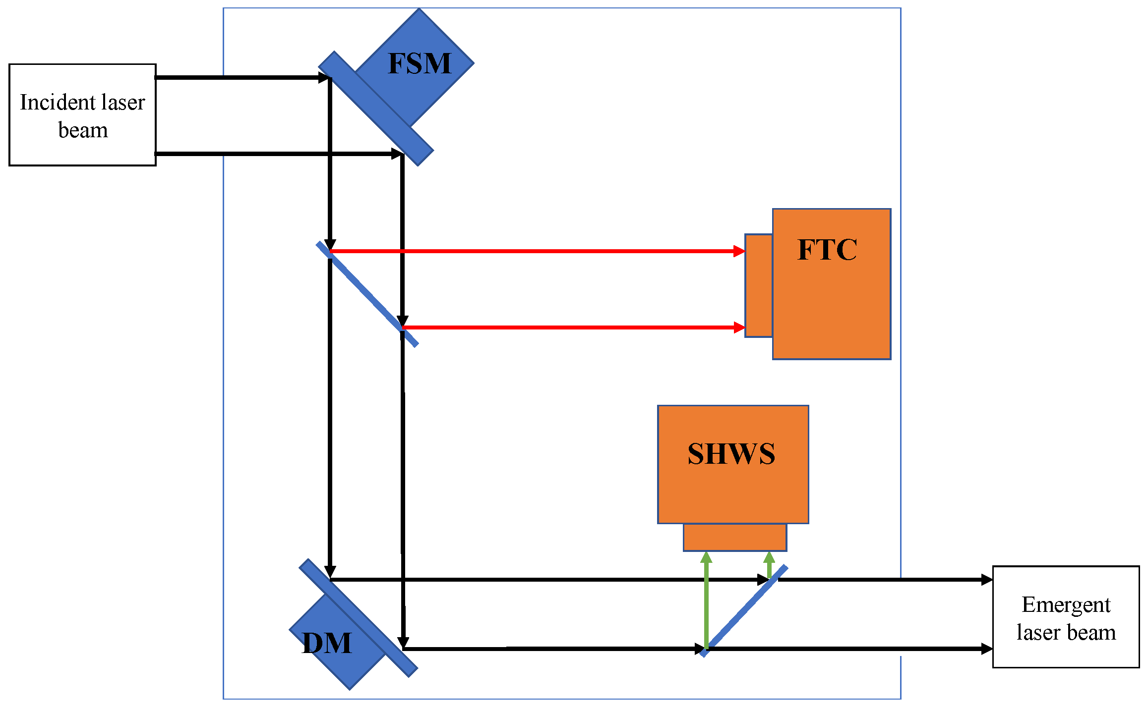
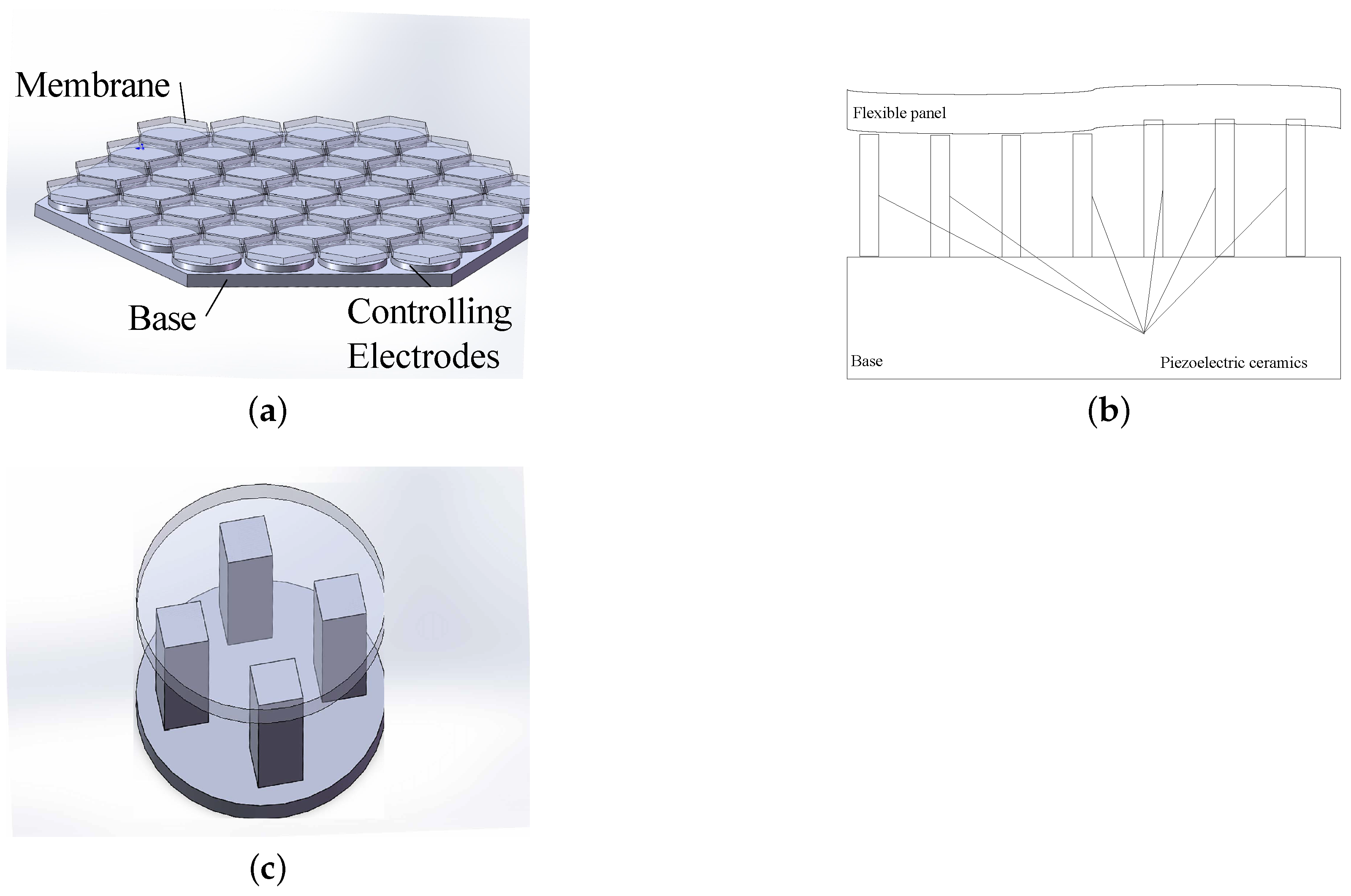
2.1. Proposed Architecture Description

The suggested AO architecture is displayed in Figure 1 which could be embedded into optical communication receiving terminals as a wavefront compensation module. When the system is powered on, an ideal incident laser beam is needed for calibration modeling. After the accomplishment of it, the terminal performs closed-loop compensation. During the procedure of closed-loop compensation, images from SHWS are passed to the wavefront controller which drives FSM and MMDM simultaneously.

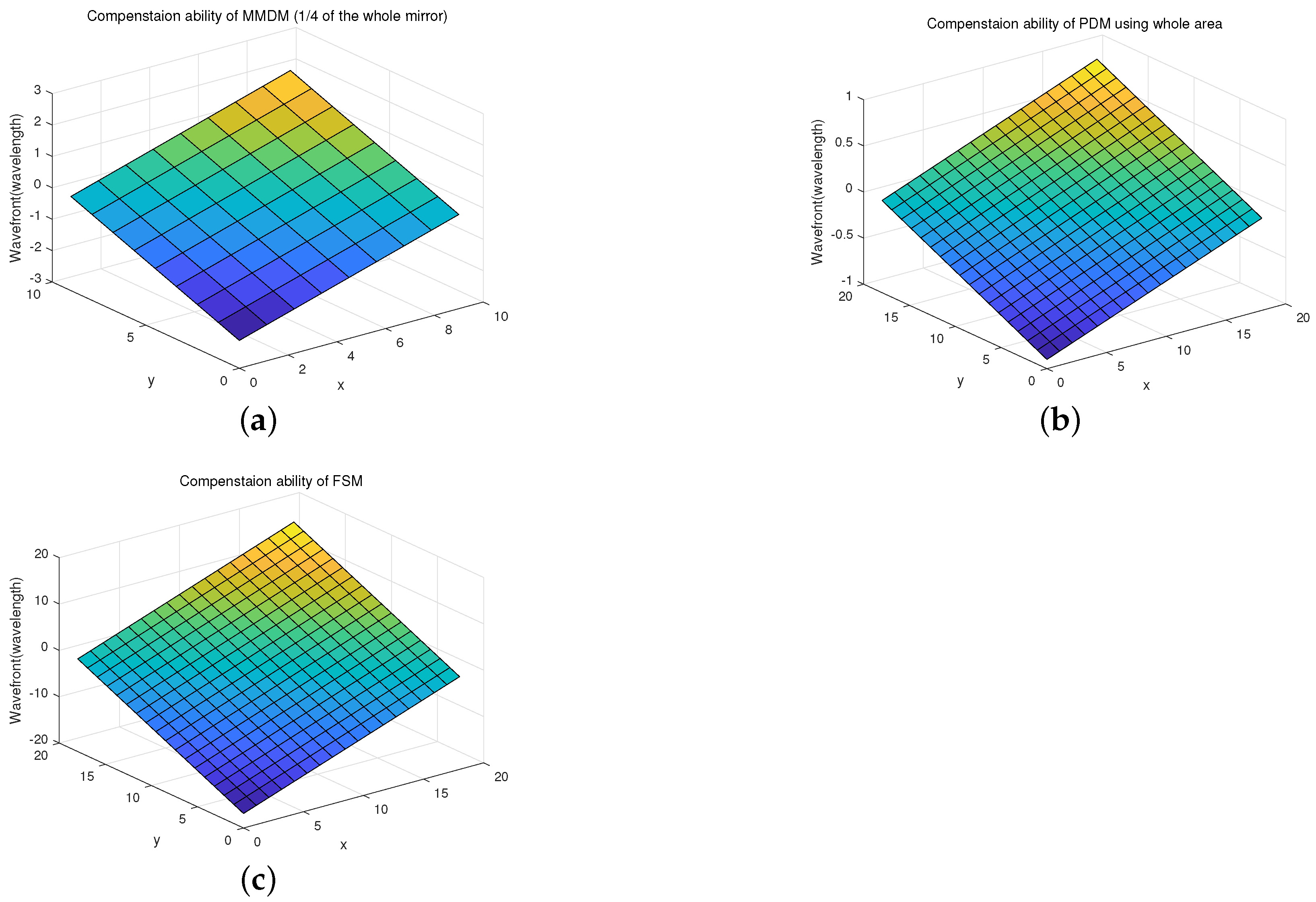
2.2. Theoretical Compensation Ability of FSM and DM Compensating Tilts Aberrations

For MMDM, the reflective surface is a static electricity controlled membrane shown in Figure 2a. Configured by the wavefront reconstructor, controlling voltages are passed to the electrodes which produce electrostatic force pulling and pushing the reflective film to form a desired shape. The advantages of MMDM lie in its cabinet size allowing it to work in a narrow environment. However, due to the absence of a physical connection between the flexible membrane and electrodes, the maximum deflection of a membrane varies from electrode to electrode. Meanwhile an inhomogeneous distribution of the tension on the mirror surface thwarts the stablization of deviation caused by marginal electrodes. Hence, the mirror could scarcely form an inclined plane to compensate tilts aberrations with the whole area. Generally the most suitable use scenario for MMDM is high-frequency compensation. As for the PDM, a brief schematic is displayed in Figure 2b. Unlike MMDM, the flexible surface is physically linked with piezoelectric ceramics. Consequently, even marginal electrodes share nearly the same rigorous mapping relationship between digital voltages configured to the electrode and stretching the measurement of the corresponding piezoelectric ceramics with the centre electrodes. Nevertheless, the physical characteristics of piezoelectric ceramics demand a hysteresis model for better precision depicting the influence of the reflective surface for the spots offsets. Owing to the balanced performance in terms of stroke and spatial resolution, it is widely used in single DM AO systems as the only wavefront corrector. For FSM, a schematic of it supported by piezoelectric ceramics is depicted in Figure 2c. It consists of a rigid non-deformable mirror. Correspondingly, the FSM cannot express any other aberrations except tilts aberrations with two controlling signals which determine the tipping and tilting angle of the mirror. Commonly, FSMs are used to either process low-order aberrations or fine tracing.
On our testbed, the diameter of MMDM is 15 mm and the number of electrodes is 37. As for the PDM, the diameter of it is 30 mm with same 37 electrodes. In addition, the FSM has two electrodes controlling a circular area with a diameter of 19 mm. According to the literature, the maximum deflection of the mirror center is 9.4 μ m. Therefore, by assuming MMDM could form an ideal tilting surface within a 90-degree sector when the center electrode is configured to the maximum stroke, 1 4 of the mirror reaches the extreme compensation scope. Represented in Figure 3a, MMDM could compensate a tilts aberrations of 4.23 wavelength at the cost of sacrificing 3 4 correction area. When electrodes are configured by the same digital voltages, the deformation of the panel shares the same magnitude. This leads to the feasibility of using the whole area to frame an inclined plane to compensate tilts aberrations. The technique documents indicate that the maximum stroke of PDM is 8 μ m. According to the simulation results shown in Figure 3b, the compensation scope of PDM is 1.8 wavelength. Similarly, the FSM can also use the whole surface to compensate tilts aberrations. Due to the non-deformable reflective surface, a literal depiction of its technical parameters focuses on inclination generation capability. According to the literature, the maximum deflection angle of FSM is 5 mrad, as shown in Figure 3c. This means a capability of 33.75 wavelength when compensating tilts aberrations.
As shown in Figure 3, the FSM has a desirable compensation ability for tipping and tilting as well as a swift response rate of 8 mrad within 1ms which is faster than higher spatial resolution wavefront corrcetors. For DMs, MMDM enjoys better local deformation ability. Besides, considering an absence of the hysteresis effect, the control of MMDM would be easier. Therefore, we cascade FSM and DM as the solution for our focused scenario.

3. High-Dynamic Atmospheric Turbulence Compensation Algorithm

In this section, we introduce our Zernike polynomials based method by which we interpret image information acquired from FSM and SHWS to wavefront phase screen so as to evaluate the quality of the incident and emergent laser beam. Secondly, a coupled second-order modeling strategy for FSM and a complete second-order modeling scheme for DM are demonstrated. Both modeling plans map controlling voltages on electrodes to offsets of spots. Subsequently, in view of the calibrated models, we apply an iterative method to solve the models obtaining optimal controlling voltages for electrodes on wavefront correctors. Finally, the workload distribution is illustrated which is the core of the high-dynamic atmospheric turbulence compensation algorithm.

3.1. Zernike Polynomials Based Phase Reconstruction Method

Collected from SHWS, the information of wavefront would be displayed in the coordinates of spots arrayed in every single aperture of the micro lens array shown in Figure 4.
By computing the offsets of the spots, the disturbance of the wavefront can be acquired. Therefore, we adopt the mapping relationship between spots offset and wavefront slopes suggested by [30]. Assume there are totally N spots on the SHWS, and let slope be the vector of partial derivatives of phase. Correspondingly, offset represents the offset vector of spots. Both slope and offset contain 2 × N elements. This process is expressed as
slope = 2 π λ f × offset
where λ stands for wavelength and f indicates focus length of micro lens array on SHWS. Furthermore, following the modal algorithm presented in [31], the coefficients of assigned Zernike terms are fitted by a least-mean-square method, yielding
A = Z T Z 1 Z T slope
where, A denotes the fitted coefficients vector and Z is the wavefront restoration matrix.

3.2. Modeling Strategy

In the context of our testbed, the wavefront reconstructor is a digital signal processor (DSP) which controls a digital-analog-converter (DAC) to produce an analog voltage of 0∼2.226 volts which is subsequently amplified to 0∼187 volts by a high voltage amplifier when controlling DM. When it comes to FSM, the 0∼2.226 volts output of DAC is amplified to 0∼10 volts. Due to the fact that the input of DAC is produced by DSP using a 24-bit data segment among which, there are 12 bits responsible for the voltage level of the output analog. Therefore, controlling voltages are expressed in a digital voltages range from 0 to 4095 within the capability of a 12-bit data segment. Literally, the relationship between the output analog voltages and input digital voltages of DAC follows Equation (3), where V a n a l o g is the level of output analog voltage, V r e f e r e n c e is the reference voltage which is 1.25 volts in our context, and V d i g i t a l represents the digital voltage.
V a n a l o g = 2 V r e f e r e n c e × V d i g i t a l 2 12
When powered on, the initial digital voltages for the DM and FSM are 2048 and 2448, respectively. Furthermore, in order to choose a reasonable stroke of the wavefront correctors, the range of digital voltages are limited to 1600 + 1600 and 400 + 400 for the DM and FSM. Additionally, we ensure the precision of the digital voltages during the process of iteration by normalizing them to 1 ∼1. Letting v i and s i represent the digital voltage and the normalized digital voltage of the ith electrode on DM or FSM, the normalization process is shown in Equation (4), where v i n i t i a l symbolises the digital voltages as our testbed is powered on 2048 for DM and 2448 for FSM. Meanwhile, v n o r m is the normalization radius of the electrodes on DM which is designed to 1600 for DM and 400 for FSM in our experiment.   
s i = ( v i v i n i t i a l ) ÷ v n o r m
Because of the attribute of DMs, the response of DMs is a function with respect to the square of controlling voltages. Nevertheless, ref. [29] points out that in practical testing, measured data are always accompanied with noise. Due to the tension of the continuous membrane introducing reflective jitter and system-level noise, the spots offsets are not exactly proportional to the square of controlling voltages. Hence, we adopt their modeling strategy adding first-order terms and constant terms to the model for more accurate fitting results. Subsequently, by assuming there are totally M electrodes on DM, the model for o f f s e t i which is the ith element in offset is shown as follows
o f f s e t i = j = 1 M a i , j × s j 2 + b i , j × s j + c i , j
where, a i , j , b i , j and c i , j symbolise coefficients of second-order terms, first-order terms, and constant terms, respectively. Additonally, the 37 electrodes are modeled one by one sequentially. During the procedure of modeling, we configure the electrodes for 10 cycles of calibration voltages, and record the spots offsets captured by SHWS. One cycle of calibration voltages contains 34 elements. Therefore, we gain 340 spots offsets vectors expressed as offset 1 offset 340 . Correspondingly, each spots offsets vector corresponds to an calibration voltage vector marked as S f u l l , 1 S f u l l , 340 . Equation (6) depicts the process of single electrode modeling.
offset 1 offset 340 = P D M × S f u l l , 1 S f u l l , 340
where, P D M is the model coefficients matrix for the currently modeled electrode.
However, when modeling the jth electrode, the constant term of it describes the comprehensive effect of all M electrodes. To handle this, we consider the contribution of each electrode on spots offsets as equal. Therefore, the kth calibration voltage vector is supposed to be designed as Equation (7)
S f u l l , k = s j , k 2 s j , k M
Referring to the above complete second-order model, we build a model for FSM containing second-order terms, first-order terms, and constant terms. In addition, considering the fact that the reflective surface of FSM is continuous and flat with tough rigidity, such characteristics would cause FSM electrodes to have a fierce coupling effect and this becomes increasingly evident when the stroke of the wavefront corrector rises. Individually building models for a single electrode and executing a linear summation cannot completely capture the effect brought by the collaboration of the two electrodes thus producing modeling errors. Correspondingly, an application of coupling terms keeps the computational complexity bearable. Meanwhile, it would not pose unaffordable burdens on solving models. The following equation is our constructed model for FSM.
o f f s e t i = a i × s 1 2 + b i × s 2 2 + c i × s 1 s 2 + d i × s 1 + e i × s 2 + f i
where, a i , b i , c i , d i , e i , f i indicate the model coefficients of the ith spots coordinate. s F S M , 1 s F S M , 2 are the called coupling terms with whom the reliability of the model bewriting the cooperation of the two electrodes is guaranteed.

3.3. Computing Controlling Voltages

Due to the nonlinearity of model as well as the overdetermination of the equation set, multiplying a pseudo-inverse of the model coefficients matrix on the left of the detected wavefront value vector could not determine an agreeable vector of controlling voltages. Therefore, the Gauss–Newton method which has the advantages of low computational complexity and excellent convergence performance is adopted.
Consider the following overdetermined equation set with 2 × N equations and M variables
offset T a r g e t = f ( s ) + e
where offset T a r g e t is the information vector collected from SHWS, and f ( s ) is a 2 × N model value vector,
s = s 1 s 2 s M T
symbolises independent variables, while e stands for an error vector.
Furthermore, the equation below is used in order to evaluate the global error of the overdetermined equation set under a certain set of solutions.
F ( s ) = 1 2 × e T e
The Gauss–Newton method solves the following optimization problem.
min s F ( s ) s . t . e = offset T a r g e t f ( s )
By repeatedly computing the step length in Equation (13) and adding it to Equation (10) until it reaches the convergence condition of Equation (11) or iteration chances are exhausted, the final Equation (10) would be denormed and configured to the electrodes of wavefront correctors.
Δ s = J T J 1 J T e
J in Equation (13) is expressed as follows,
J = e 1 s 1 e 1 s M e 2 N s 1 e 2 N s M .
In practical applications, the Gauss–Newton method runs as Algorithm 1
Algorithm 1: A description of the Guass–Newton method
1:
Initializing s to zero vector.
2:
Acquiring o f f s e t T a r g e t from SHWS.
3:
Computing f ( s ) according to model and s .
4:
Computing e in Equation (9).
5:
Checking whether e reaches the convergent criterion. If it does, exiting the algorithm and configuring controlling voltages to electrodes, otherwise computing J in Equation (14).
6:
Computing Δ s in Equation (13) then updating s in Equation (10).
7:
Checking whether it exhausts iteration chances. If it does, exiting the algorithm and configuring controlling voltages to electrodes, otherwise returning back to process 3.

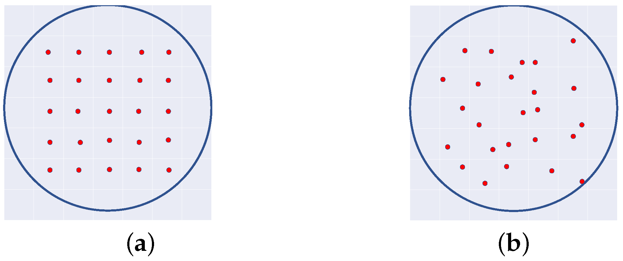
3.4. Capturing Aberrations

In the previous subsection, we apply the Gauss–Newton method to compute controlling voltages for the electrodes of wavefront correctors. However, an input is supposed to be provided as the target of iteration which is the offset T a r g e t in Equation (9). In this subsection, we introduce our method of providing input for the Gauss–Newton method.
For single DM AO architecture, all workloads are put on the only wavefront corrector. Traditional iterative wavefont correction algorithms building on the relationship between controlling voltages and spots offsets linearly combine current spots offsets, wavefront residual of the previous turn and model value as offset T a r g e t . The algorithm captures accurate wavefront aberrations and according to [29], the wavefront residual remains under 1 8 w a v e l e n g t h after compensation. Nevertheless, in double wavefront correctors architecture, distribution of the workload on FSM and DM separately determines the precision of the compensated results.
In order to divide the labor of woofer and tweeter which are the FSM and DM in our context, the Lagrange-multiplier method [23,24] multiplied a multiplier λ to the left of the response matrix of tweeter as shown in Equation (15)
offset = P w o o f e r × s w o o f e r + λ P t w e e t e r × s t w e e t e r
where P w o o f e r and P t w e e t e r are response matrices for the woofer and tweeter, while s w o o f e r and s t w e e t e r are actuator vectors for the woofer and tweeter. The basic solving process are expressed in Equation (16)
P w o o f e r T P w o o f e r λ P w o o f e r T P t w e e t e r λ P t w e e t e r T P w o o f e r λ 2 P t w e e t e r T P t w e e t e r s w o o f e r s t w e e t e r = P w o o f e r T λ P t w e e t e r T offset
However, by marking [ P w o o f e r λ P t w e e t e r ] as P g l o b a l , the irreversibility of P g l o b a l T P g l o b a l determines that a damped least-square method is needed for solving actuator vectors as shown in Equation (17).
s w o o f e r s t w e e t e r = P w o o f e r T P w o o f e r + β 1 λ P w o o f e r T P t w e e t e r λ P t w e e t e r T P w o o f e r λ 2 P t w e e t e r T P t w e e t e r + β 2 1 P w o o f e r T λ P t w e e t e r T offset
where β 1 and β 2 are damping parameter matrices. In Equation (17), λ , β 1 and β 2 are manually set. The empirically selected λ can suppress coupling between the woofer and tweeter. However, Equation (15) is neither a necessary nor sufficient condition for decoupling high and low-order aberrations.
By contrast, in our FSM-DM cascaded AO architecture, the workload of FSM and DM consists of decoupled current spots offsets, decoupled wavefront residual of the previous turn and model value. Model value can be computed with coefficient matrices and current controllilng voltages. Decoupled current spots offsets and decoupled wavefront residual of the previous turn are acquired from current spots offsets and wavefront residual. By changing them to wavefront slopes using Equation (1) the coefficients of Zernike polynomials can be fitted with Equation (2). Subsequently, after separated Zernike coefficients performing the inverse process of Equations (1) and (2) in turn, the decoupled current spots offsets, and the decoupled wavefront residual of the previous turn can be gained. It should be noted that, the current spots offsets are calculated from the current wavefront on SHWS while the wavefront residuals are acquired from the compensated wavefront output of the previous turn on SHWS.
According to [32], consider the 2nd and 3rd order of Zernike polynomials in Cartesian coordinate system marked as Zernike 2 and Zernike 3 , as shown in Equation (18).
Zernike 2 = 2 x , Zernike 3 = 2 y ,
where x and y are coordinate vectors within the normalized area. The formulas above reveal that the 2nd and 3rd of the Zernike polynomials vary monotonically with x and y . They depict the horizontal and vertical tilt of the phase screen which demands barely any capability of local deformation. This fits the deformation capability of FSM shown in Figure 3c which forms a tilt shape with a spatial resolution of two. In contrast, the phase screens described by the fourth and above Zernike polynomials are not a plane, for example, the 4th∼6th order of Zernike polynomials in Equation (19). There are local fluctuations in the phase screen, which require a higher spatial resolution to be expressed. Therefore, the workload allocated to FSM is to compensate the 2nd and 3rd order Zernike aberrations while the rest of the wavefront aberrations belong to the DM.
Zernike 4 = 2 3 ( x 2 + y 2 ) 3 , Zernike 5 = 2 6 x y , Zernike 6 = 6 ( x 2 y 2 )
Assuming the coefficients of Zernike polynomials are,
a = [ a 2 , a 3 , , a 15 ] T
where subscripts symbolise order. Decoupled offsets expressed in o f f s e t D e c o u p l e d , l o w and o f f s e t D e c o u p l e d , h i g h (tilts aberrations and high-order aberrations, respectively) are gained according to the following procedure.
offset D e c o u p l e d , L o w = Z × I L o w × a ÷ 2 π λ f
offset D e c o u p l e d , H i g h = Z × I H i g h × a ÷ 2 π λ f
where, Z is the wavefront restoration matrix which corresponds to 2 nd 15 th order Zernike polynomials, while I L o w and I H i g h are shown as follows
I L o w = 1 1 0 0 , I H i g h = 0 0 1 1
Denoting offset with a subscript containing ‘ l o w ’ as spots offsets caused by low-order aberrations while offset with a subscript containing ‘ h i g h ’ as spots offsets caused by high-order aberrations. Representing iterative target as offset D e c o u p l e d , L o w , T a r g e t and offset D e c o u p l e d , H i g h , T a r g e t , they are set as follows
offset D e c o u p l e d , L o w , T a r g e t = f F S M ( s F S M ) + ( offset D e c o u p l e d , L o w , R e s i d u a l ) + ( offset D e c o u p l e d , L o w , D e t e c t e d )
offset D e c o u p l e d , H i g h , T a r g e t = f D M ( s D M ) + ( offset D e c o u p l e d , H i g h , R e s i d u a l ) + ( offset D e c o u p l e d , H i g h , D e t e c t e d )
where f F S M ( s F S M ) and f D M ( s D M ) illustrate model values, offset D e c o u p l e d , L o w , R e s i d u a l and offset D e c o u p l e d , H i g h , R e s i d u a l are the decoupled wavefront residual of the previous turn, while offset D e c o u p l e d , L o w , D e t e c t e d and offset D e c o u p l e d , H i g h , D e t e c t e d are decoupled current spots offsets.
As we are expected to drive the wavefront correctors eliminating the detected offsets, the target should be set opposite to the decoupled current spots or decoupled wavefront residual.
The above method effectively suppresses the wavefront residual and distributes the workload. Meanwhile, it saves the stroke of DM by passing the pressure of the stroke to FSM.

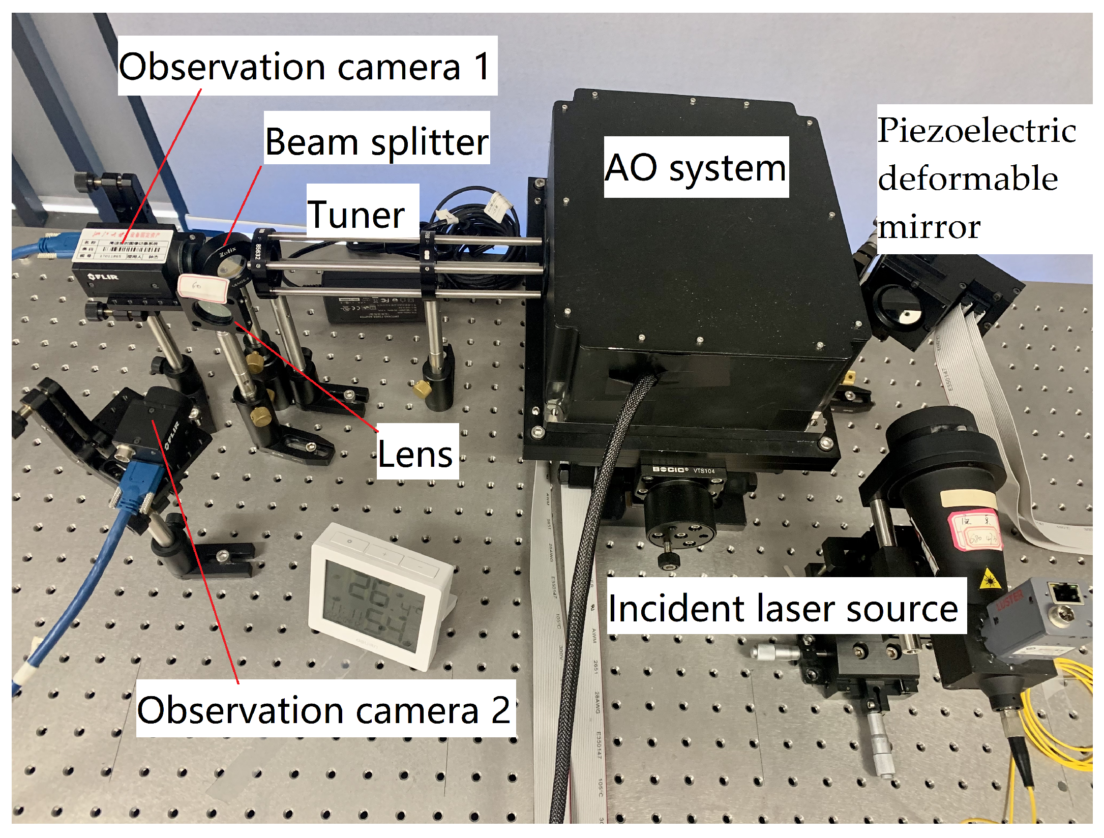
4. Implementation and Experimental Results

In this section, we introduce the implementation of the calibration modeling as well as the simulative performance of our algorithm.

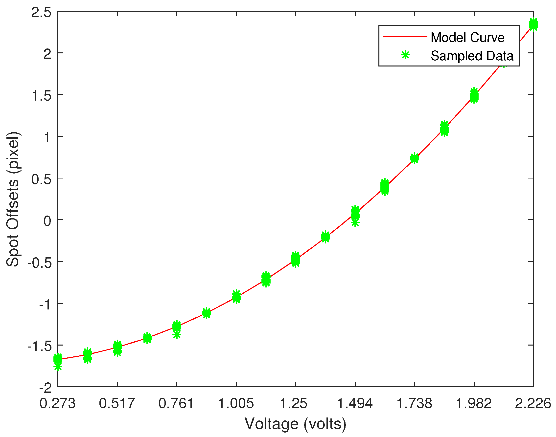
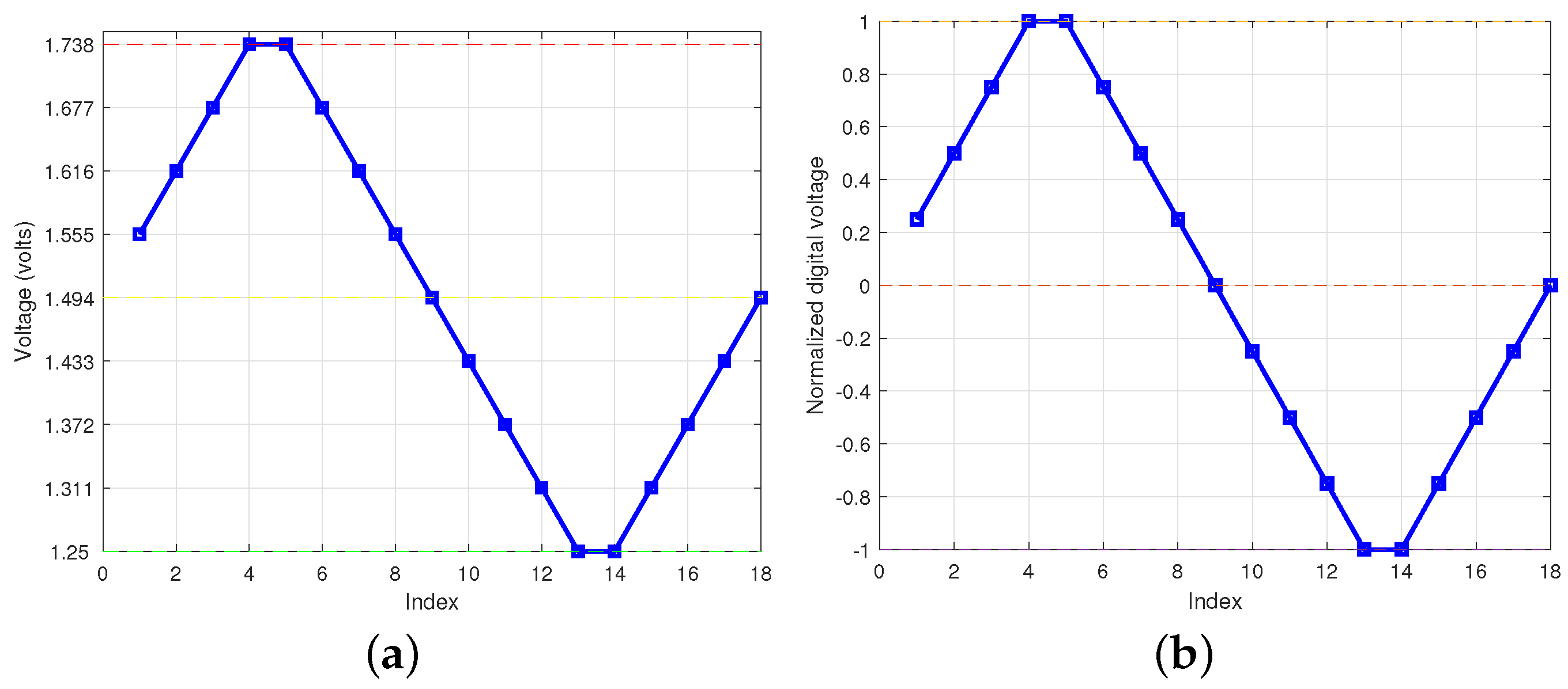
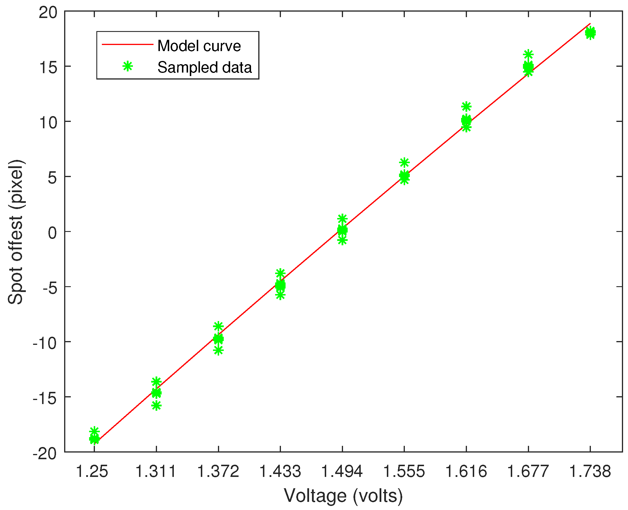
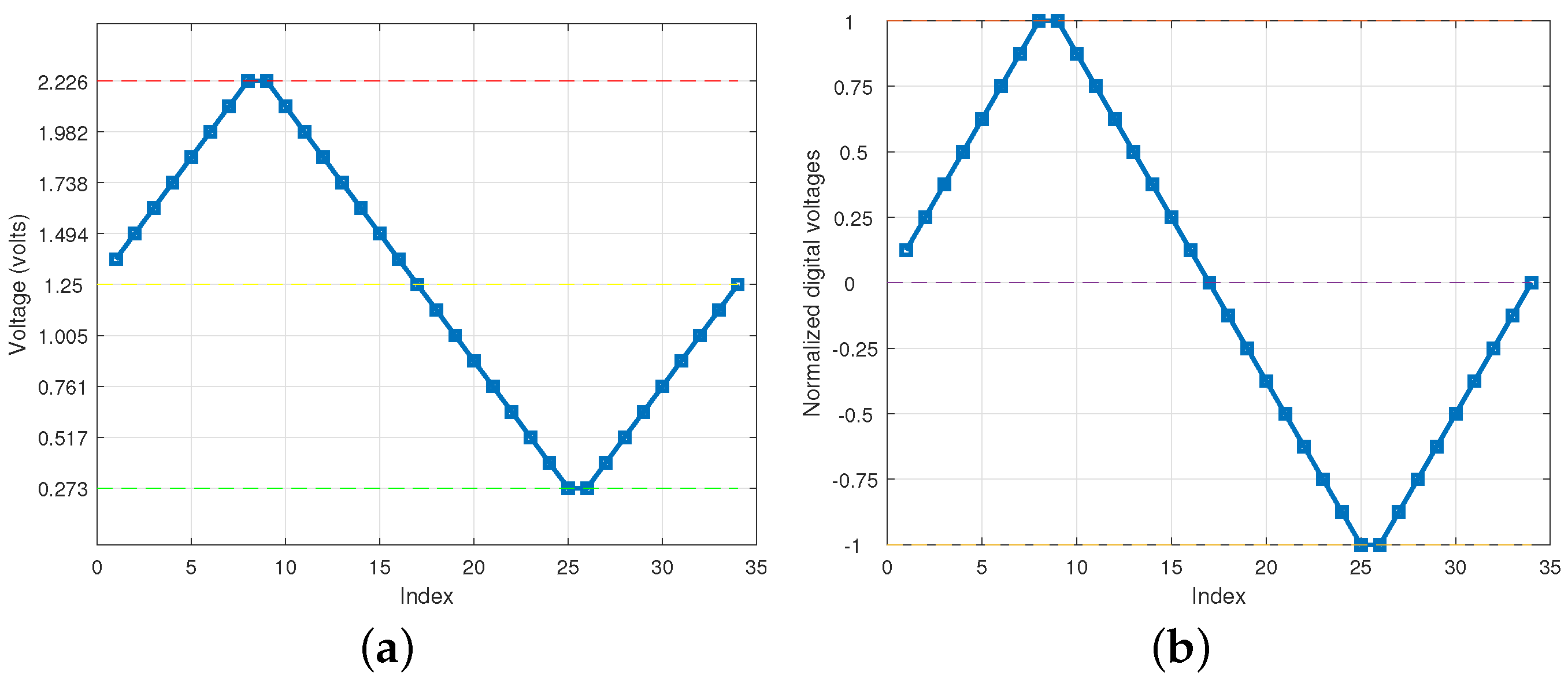
4.1. Calibration Modeling

The modeling procedure is examined on our testbed displayed in Figure 5, from which we gain the coefficient matrices of DM and FSM describing the mapping relationship between spots offsets and controlling voltages. On our testbed, a 800 nm wavelength laser beam with a diameter of 15 mm is used as the ideal incident light. As for the AO system, the internal topology is shown in Figure 1. Within it, the wavefront sensor is a charge coupled device (CCD) camera with a micro lens array covered in the front of it which has a focus of 18.8 mm. Moreover, the effective area of the wavefornt sensor contains 1088 × 1088 pixels whose size is 5.5 μ m, while the size of a single aperture of the micro lens array is 300 μ m which means the wavefont sensor can capture spots in an around 19 × 19 rectangle area. However, in our experiment environment, the detected spots on the wavefront sensor cover a circular area with a diameter of 17 apertures. Additionally, the PDM in front of the light entrance is not drived on the current stage and it is set for a future experiment. On the left of the AO system, devices are depolyed for observing the emitting light.
For DM, the calibration voltages in one period are shown in Figure 6. During the process of modeling the DM, we repeatedly configure the calibration voltages on every electrode for 10 periods. Each calibration voltage produces 20 data samples (two data per period). After receiving the 20 data samples, we use the least square method to solve pre-term coefficients for the current affecting electrode. The calibration voltages take 200 as the step and 2048 as center, traversing the voltage range of ± 1600 . According to Equation (3), a digital voltage ranging from 448 to 3648 can be linearly interpreted to an analog voltage ranging from 0.273 volts to 2.226 volts.
Figure 7 displays the favorable fitting result of the first electrode for the x coordinate of the 111st spot. It indicates that a maximum modeling error of 0.05 pixels exists in the system which is kept under an acceptable threshold.
Different from the modeling structure of the DM, the structure of FSM contains coupling terms depicting the collaborative effects of electrodes on spots offsets. This leads to the requirement that when modeling, the two electrodes should be modeled together. Therefore, the horizontal electrode is sequentially configured with a period of calibration voltages. Whenever the horizontal electrode is configured with a calibration voltage, the vertical electrode is configured with a period of calibration voltages in turn. Furthermore, due to the large maximum stroke of FSM, the used range of it is limited to ± 400 in digital voltages, as displayed in Figure 8.
Figure 9 shows the fitting result of the fitting condition of the model for the spot offsets of the first spot. As is demonstrated in the figure, a maximum modeling error of 0.9 pixels shows up which is still within the acceptable range.

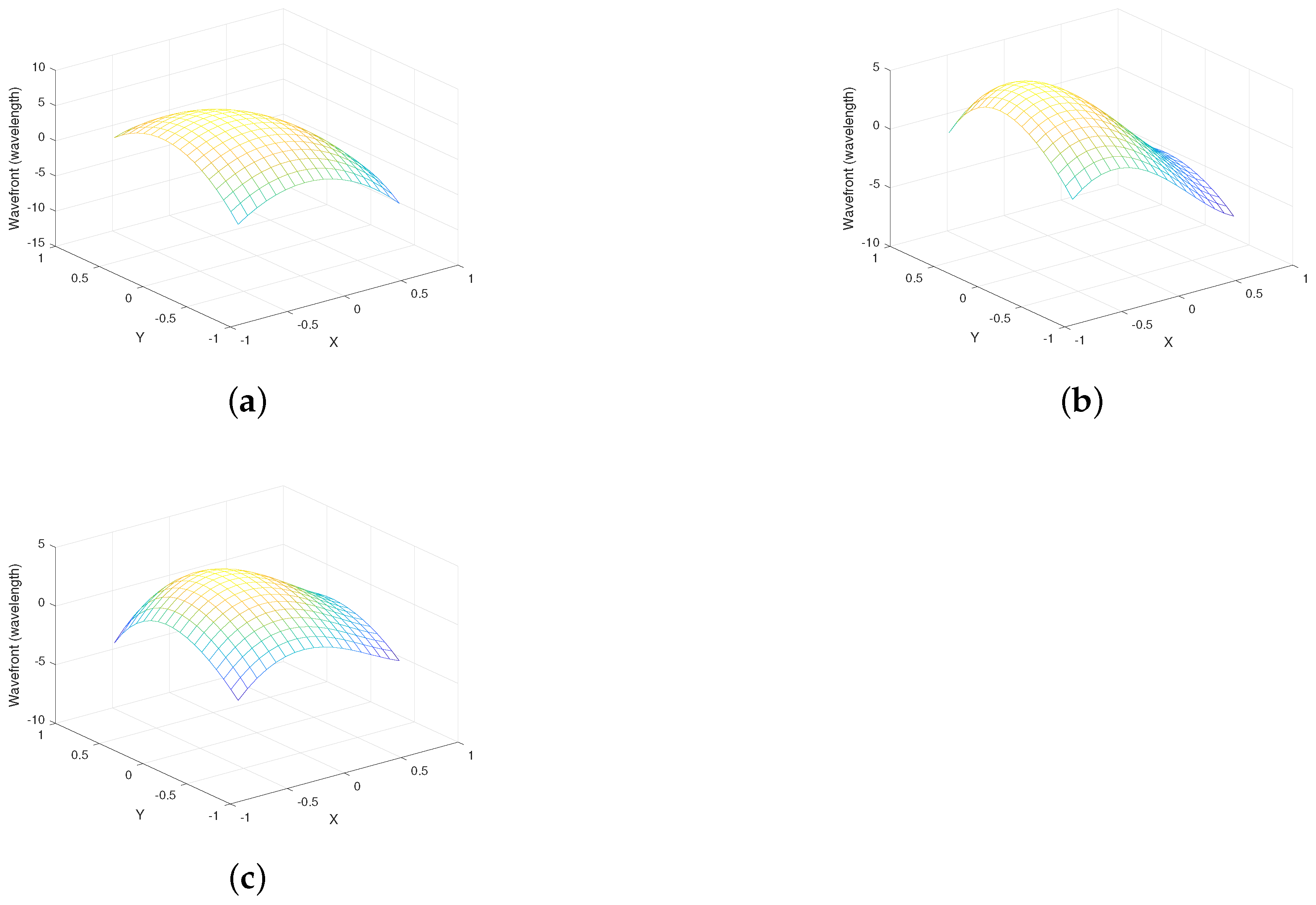
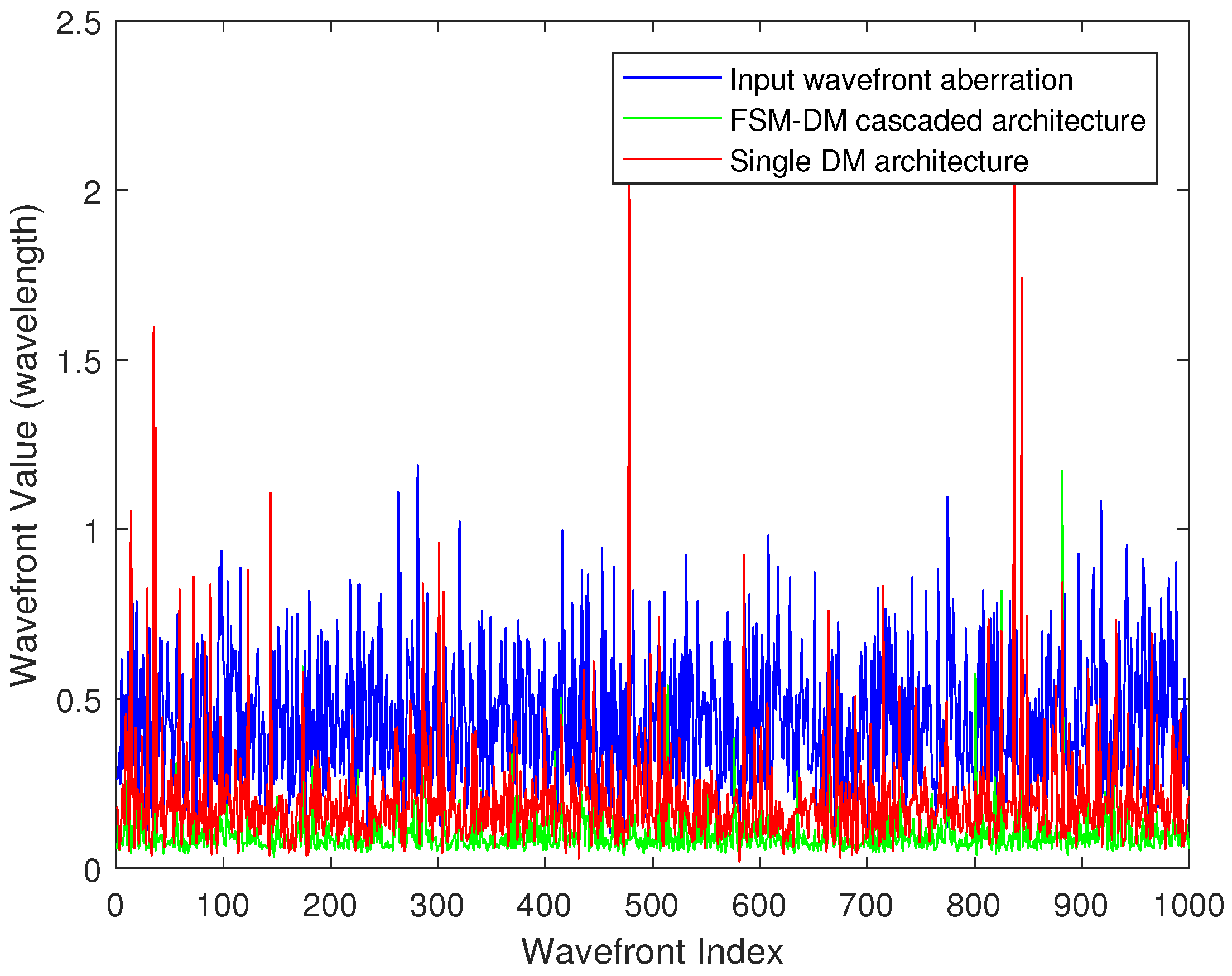
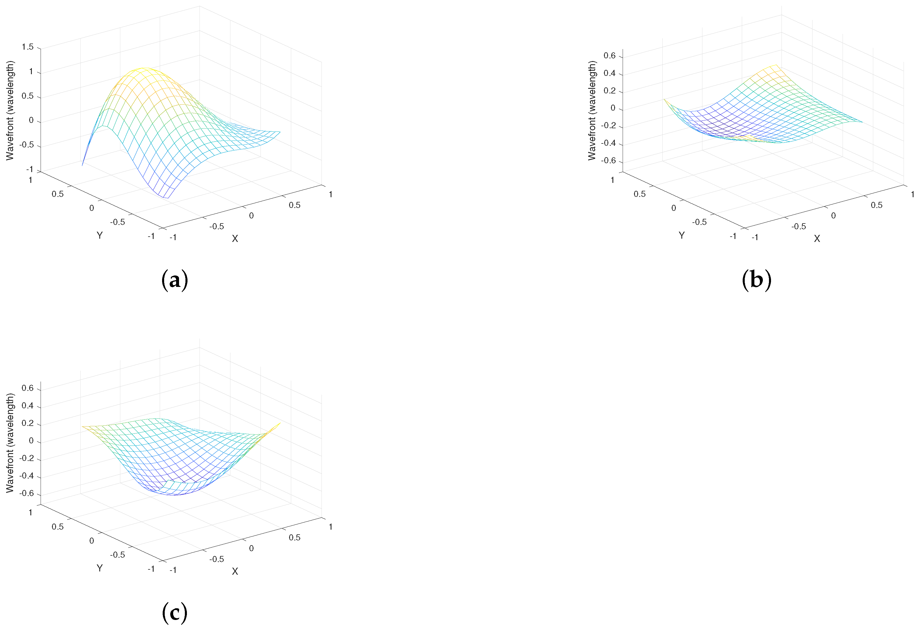
4.2. Simulation Results

Firstly, we examine the Zernike mode decomposition method by driving FSM-DM cascaded AO architecture and single DM architecture approaching our generated phase screen. The result presented in Figure 10 illustrates that when approaching a phase screen containing tilts aberrations, FSM-DM cascaded AO architecture can form a surface shape that is closer to the generated phase screen than the single-DM AO architecture. The PV of Figure 10a is 15.76 wavelength. As for Figure 10b,c, the PV values are 10.99 wavelength and 6.75 wavelength, respectively. Furthermore, due to the response rate of the FSM, the FSM-DM cascaded AO architecture is bound to have a swifter response towards tilts aberrations.
Secondly, to illustrate the merits of FSM-DM cascaded AO architecture against single DM AO architecture, we produced a single phase screen as the input wavefornt according to the Kolmogorov theory [32]. Subsequently, generated phase screen is interpreted to spots offsets which is the direct information we can gain from the wavefront of our sensor. Finally, we observe the phase screen before compensation, phase screens compensated by FSM-DM cascaded AO architecture, and single DM architecture. The result is shown in Figure 11.
Figure 11a shows the simulative input wavefront of the system where a peak phase value of 1.13 wavelength can be generated while the valley phase value is −0.953 wavelength. After the compensation of FSM-DM cascaded AO architecture with the proposed algorithm, the convergent phase plane reaches a peak phase value of 0.196 wavelength and a valley phase value of −0.158 compared to single DM AO architecture with the traditional algorithm whose reconstructed phase plane claims a peak phase value of 0.360 wavelength and a valley phase value of −0.302 wavelength. In addition, although both the suggested and traditional architecture can compensate wavefont aberrations, the reconstructed phase planes demonstrate that the results produced by raised architecture with raised algorithms are more gentle which reflects the necessity of an FSM.
In addition, by analysing the iterative procedure of compensating a single wavefront input, Figure 12 reveals that for a wavefront input of 0.53 wavelength, both FSM-DM cascaded architecture and single DM AO architecture converges using the iterative compensation algorithm within one iteration. Nevertheless, as for the convergence level, single DM architecture converges to 0.12 wavelengths after compensation compared to the results of our proposed architecture which is approaching 0.09 wavelengths.
Another verification for the consecutive compensating capability of our architecture with the algorithm is conducted. Firstly, a series of discrete phase screens according to Kolmogorov theory [32] are produced. Additionally, in order to simulate a dynamic atmospheric turbulence disturbed phase screen, we perform interpolation using a parallel temporal filter following [33] and produce 1000 distorted wavefront inputs in total. During the process, Zernike polynomials are also used to mathematically represent phase screens and change them to spots offsets. The results are shown in Figure 13.
The figure consists of three curves representing input wavefront aberrations, wavefront residuals compensated by single DM architecture, and wavefront residuals compensated by FSM-DM cascaded architecture. The blue curve represents the wavefront value when the laser beam has not been compensated by any AO system, which is also the quality of optical communication without the AO system in FSO communications. It fluctuates from around 1 5 to 4 5 wavelength which in our context is 1.6 μ m to 6.4 μ m. By contrast, considering the red curve in Figure 13, it represents the compensation performance of traditional AO architecture which contains only one DM. The curve fluctuates around 1 6 1 10 wavelength with sharp glitches which occur because the model of DM cannot depict the overwhelmingly large tilts aberrations within the effective arguments range leading to a divergent result. This fact also demonstrates the advantage of FSM deployed in front of the DM with which the probability of divergence caused by parameter range limits are fully supressed. As shown in Figure 13, apart from the above curves, a green curve illustrates the stable tendency of wavefront residuals under 1 16 wavelength which is also displayed. Although, there are glitches, the reasons for their occurence lies in the coupling of tilts aberrations with high-order aberrations in the DM model. A calibration modeling strategy truthfully reflects the mapping relationship of spots offsets with voltages configured on the electrodes, however, tilts aberrations and high-order aberrations are coupled in the DM model. This demands the DM shoulder a part of the workload for tilts aberrations when conducting wavefront compensation. When generating random wavefront input using the DM model, the proportion of the tilt aberration of certain groups of inputs will be relatively high. As this part of the tilt aberrations are distributed to the workload of FSM, the glitch appears in the compensation of the remaining workload by the DM.

5. Conclusions

In conclusion, this paper clarifies the use of Zernike mode decomposition to decompose wavefronts into 2nd, 3rd and 4th∼15th orders which are compensated by FSM and DM, respectively. The decomposition ensures the compensation capability of FSM-DM cascade AO architecture. Meanwhile, modeling strategies of FSM and DM and the iterative compensation algorithm guarantee the precision of the compensation. In addition, the performance of the algorithm has been simulatively verified. For compensating a static input wavefront, the wavefornt residuals are better supressed around 1 16 wavelength than 1 6 wavelength for single DM AO architecture. Conversely, for consecutively compensating the Kolmogorov theory-based dynamic atmospheric turbulence disturbed incident laser beam, the algorithm reaches a convergence level under 1 16 wavelength better than 1 10 to 1 6 for the single AO architecture when glitches are not counted. This study intends to provide a guideline to design the AO architecture for future FSO communications.

Author Contributions

Conceptualization, investigation and methodology—J.Z. and S.Y.; experimentation, data acquisition and analysis—H.M. and X.Y.; writing-original draft preparation—H.M. and J.Z.; writing-review and editing—J.Z., G.L. and P.X. All authors have read and agreed to the published version of the manuscript.

Funding

This research was funded by the Key Project of Science and Technology of Hainan (No. ZDKJ2019003) and the Major Key Project of PCL (PCL2021A03-1).

Institutional Review Board Statement

Not applicable.

Informed Consent Statement

Not applicable.

Data Availability Statement

The data presented in this study are available on request from the corresponding author. The data are not publicly available due to privacy issues.

Conflicts of Interest

The authors declare no conflict of interest.

References

  1. Khalighi, M.A.; Uysal, M. Survey on Free Space Optical Communication: A Communication Theory Perspective. IEEE Commun. Surv. Tutor. 2014, 16, 2231–2258. [Google Scholar] [CrossRef]
  2. Tian, Y.; Zhong, J.; Lin, X.; Xiao, P.; Yang, H.; Zhong, Y.; Kang, D. High-dynamic wavelength tracking and millimeter-level ranging inter-satellite laser communication link with feedback-homodyne detection. Appl. Opt. 2019, 58, 5687–5694. [Google Scholar] [CrossRef] [PubMed]
  3. Zhu, X.; Kahn, J.M. Free-space optical communication through atmospheric turbulence channels. IEEE Trans. Commun. 2002, 50, 1293–1300. [Google Scholar] [CrossRef]
  4. Andrews, L.C.; Phillips, R.L. Society of Photo-optical Instrumentation Engineers. In Laser Beam Propagation through Random Media; SPIE: Bellingham, WA, USA, 2005. [Google Scholar]
  5. Weyrauch, T.; Vorontsov, M. Free-space laser communications with adaptive optics: Atmospheric compensation experiments. J. Optic. Commun. Rep. 2004, 1, 355–379. [Google Scholar] [CrossRef]
  6. Tyson, R.K. Bit-error rate for free-space adaptive optics laser communications. J. Opt. Soc. Am. A 2002, 19, 753–758. [Google Scholar] [CrossRef] [PubMed]
  7. Gregory, M.; Troendle, D.; Muehlnikel, G.; Heine, F.; Meyer, R.; Lutzer, M.; Czichy, R. Three years coherent space to ground links: Performance results and outlook for the optical ground station equipped with adaptive optics. In Proceedings of the Free-Space Laser Communication and Atmospheric Propagation XXV, San Francisco, CA, USA, 2–7 February 2013; Volume 8610, pp. 17–29. [Google Scholar] [CrossRef]
  8. Roberts, W.T.; Antsos, D.; Croonquist, A.; Piazzolla, S.; Roberts, L.C., Jr.; Garkanian, V.; Trinh, T.; Wright, M.W.; Rogalin, R.; Wu, J.; et al. Overview of Ground Station 1 of the NASA space communications and navigation program. In Proceedings of the Free-Space Laser Communication and Atmospheric Propagation XXVIII, San Francisco, CA, USA, 13–18 February 2016; Volume 9739, pp. 82–99. [Google Scholar] [CrossRef]
  9. Petit, C.; Vedrenne, N.; Michau, V.; Artaud, G.; Issler, J.-L.; Samain, E.; Toyoshima, M.; Akioka, M.; Kolev, D.; Munemasa, Y.; et al. Adaptive optics results with SOTA. In Proceedings of the 2015 IEEE International Conference on Space Optical Systems and Applications (ICSOS), New Orleans, LA, USA, 26–28 October 2015; pp. 1–7. [Google Scholar] [CrossRef]
  10. Ezhov, V.; Vasilieva, N.; Ivashkin, P.; Galstian, A. Toward a locally adaptive optical protection filtering for human eyes and technical vision sensors. Appl. Opt. 2020, 59, B1–B9. [Google Scholar] [CrossRef]
  11. Ma, J.; Li, Y.; Yu, Q.; Yang, Z.; Hu, Y.; Chu, J. Generation of High-Quality Tunable Airy Beams with an Adaptive Deformable Mirror. Opt. Lett. 2018, 43, 3634–3637. [Google Scholar] [CrossRef]
  12. Booth, M. Adaptive optical microscopy: The ongoing quest for a perfect image. Light Sci. Appl. 2014, 3, e165. [Google Scholar] [CrossRef]
  13. Ruppel, T.; Dong, S.; Rooms, F.; Osten, W.; Sawodny, O. Feedforward Control of Deformable Membrane Mirrors for Adaptive Optics. IEEE Trans. Control Syst. Technol. 2013, 21, 579–589. [Google Scholar] [CrossRef]
  14. Dayton, D.; Pierson, B.; Spielbusch, B.; Gonglewski, J. Atmospheric structure function measurements with a Shack–Hartmann wave-front sensor. Opt. Lett. 1992, 17, 1737–1739. [Google Scholar] [CrossRef]
  15. Wang, Y.; Chen, X.; Cao, Z.; Zhang, X.; Liu, C.; Mu, Q. Gradient cross-correlation algorithm for scene-based Shack-Hartmann wavefront sensing. Opt. Express 2018, 26, 17549–17562. [Google Scholar] [CrossRef] [PubMed]
  16. Nam, J.; Thibos, L.N.; Bradley, A.; Himebaugh, N.; Liu, H. Forward light scatter analysis of the eye in a spatially-resolved double-pass optical system. Opt. Express 2011, 19, 7417–7438. [Google Scholar] [CrossRef] [PubMed]
  17. Zhao, S.M.; Leach, J.; Gong, L.Y.; Ding, J.; Zheng, B.Y. Aberration corrections for free-space optical communications in atmosphere turbulence using orbital angular momentum states. Opt. Express 2012, 20, 452–461. [Google Scholar] [CrossRef] [Green Version]
  18. Dalimier, E.; Dainty, C. Comparative analysis of deformable mirrors for ocular adaptive optics. Opt. Express 2005, 13, 4275–4285. [Google Scholar] [CrossRef] [PubMed]
  19. Chen, X.; Wang, C.; Zheng, L.; Cai, J.; Ding, Y. Measurement of interactive matrix and flat-surface calibration of OKO 109-channel deformable mirror using ZYGO-GPI interferometer. In Proceedings of the Optical Metrology and Inspection for Industrial Applications VII, Online, 11–16 October 2020; Volume 11552, pp. 363–366. [Google Scholar] [CrossRef]
  20. Ma, J.; Chen, K.; Chen, J.; Li, B.; Chu, J. Closed-loop correction and ocular wavefronts compensation of a 62-element silicon unimorph deformable mirror. Chin. Opt. Lett. 2015, 13, 042201. [Google Scholar]
  21. Vdovin, G. Closed-loop adaptive optical system with a liquid mirror. Opt. Lett. 2009, 34, 524–526. [Google Scholar] [CrossRef] [PubMed]
  22. Ran, B.; Yang, P.; Wen, L.; Du, R.; Yang, K.; Wang, S.; Xu, B. Design and analysis of a reactionless large-aperture fast steering mirror with piezoelectric actuators. Appl. Opt. 2020, 59, 1169–1179. [Google Scholar] [CrossRef]
  23. Zou, W.; Qi, X.; Burns, S.A. Wavefront-aberration sorting and correction for a dual-deformable-mirror adaptive-optics system. Opt. Lett. 2008, 33, 2602–2604. [Google Scholar] [CrossRef] [Green Version]
  24. Zou, W.; Qi, X.; Burns, S.A. Woofer-tweeter adaptive optics scanning laser ophthalmoscopic imaging based on Lagrange-multiplier damped least-squares algorithm. Biomed. Opt. Express 2011, 2, 1986–2004. [Google Scholar] [CrossRef] [Green Version]
  25. Yang, S.; Ke, X. Experimental study on adaptive optical wavefront correction with dual mirrors in free space optical communication. Optik 2021, 242, 167146. [Google Scholar] [CrossRef]
  26. Hu, S.; Xu, B.; Zhang, X.; Hou, J.; Wu, J.; Jiang, W. Double-deformable-mirror adaptive optics system for phase compensation. Appl. Opt. 2006, 45, 2638–2642. [Google Scholar] [CrossRef] [PubMed]
  27. Liu, W.; Dong, L.; Yang, P.; Lei, X.; Yan, H.; Xu, B. A Zernike mode decomposition decoupling control algorithm for dual deformable mirrors adaptive optics system. Opt. Express 2013, 21, 23885–23895. [Google Scholar] [CrossRef] [PubMed]
  28. Kong, L.; Cheng, T.; Yang, P.; Wang, S.; Yang, C.; Zhao, M. Decoupling control algorithm based on numerical orthogonal polynomials for a woofer-tweeter adaptive optics system. Opt. Express 2021, 29, 22331–22344. [Google Scholar] [CrossRef] [PubMed]
  29. Yu, W.; Zhong, J.; Chen, G.; Mao, H.; Yang, H.; Zhong, Y. Wavefront correction algorithm based on a complete second-order DM-SHWS model for free-space optical communications. Appl. Opt. 2021, 60, 4954–4963. [Google Scholar] [CrossRef]
  30. Zhu, L.; Sun, P.; Bartsch, D.; Freeman, W.R.; Fainman, Y. Adaptive control of a micromachined continuous-membrane deformable mirror for aberration compensation. Appl. Opt. 1999, 38, 168–176. [Google Scholar] [CrossRef]
  31. Southwell, W.H. Wave-front estimation from wave-front slope measurements. J. Opt. Soc. Am. 1980, 70, 998–1006. [Google Scholar] [CrossRef]
  32. Roddier, N. Atmospheric wavefront simulation and Zernike polynomials. Opt. Eng. 1990, 29, 1174–1180. [Google Scholar]
  33. Zhang, Y.; Zhong, J.; Yu, W.; Chen, G.; Guo, P. A hybrid spatial-temporal laser beam wavefront emulator with flexible resolution. In Proceedings of the IEEE International Conference on Space Optical Systems and Applications, Portland, OR, USA, 14–16 October 2019. [Google Scholar]
Figure 1. Proposed AO architecture.
Network 02 00018 g001
Figure 2. (a) Schematic section of the micromachined membrane deformable mirror. (b) Schematic section of the piezoelectric deformable mirror. (c) Schematic section of the fast steering mirror.
Network 02 00018 g002
Figure 3. (a) Theoretical compensation ability of 1 4 MMDM for tilts aberrations. (b) Theoretical compensation ability of PDM for tilts aberrations. (c) Theoretical compensation ability of FSM for tilts aberrations.
Network 02 00018 g003
Figure 4. (a) Spots distribution on SHWS without distortion. (b) Spots distribution on SHWS with distortion.
Network 02 00018 g004
Figure 5. Photograph of the setup.
Network 02 00018 g005
Figure 6. (a) Calibration voltages for DM constructing models in one period. (b) Normalized calibration voltages for DM constructing models in one period.
Network 02 00018 g006
Figure 7. The fitting curve of the first electrode for the x coordinate of the 111st spot.
Network 02 00018 g007
Figure 8. (a) Digital calibration voltages for FSM constructing models in one period. (b) Normalized calibration voltages for FSM constructing models in one period.
Network 02 00018 g008
Figure 9. The fitting curve of both electrodes for the x coordinate of the 1st spot.
Network 02 00018 g009
Figure 10. (a) A generated phase screen. (b) FSM-DM cascaded architecture approaching the generated phase screen. (c) Single DM architecture approaching the generated phase screen.
Network 02 00018 g010
Figure 11. (a) Wavefront before compensation. (b) Wavefront compensated by proposed FSM-DM cascaded AO architecture with suggested algorithm. (c) Wavefront compensated by single DM AO architecture with traditional algorithm.
Network 02 00018 g011
Figure 12. The variation of the wavefont RMS value when compensating a single wavefront input with proposed AO architecture and single DM AO architecture.
Network 02 00018 g012
Figure 13. Compensation results of the wavefront RMS value by FSM-DM cascaded architecture and single DM architecture.
Network 02 00018 g013
Publisher’s Note: MDPI stays neutral with regard to jurisdictional claims in published maps and institutional affiliations.

