Automated SILAR System for High-Precision Deposition of CZTS Semiconductor Thin Films

 ,
, 
Abstract
1. Introduction
2. Materials and Methods
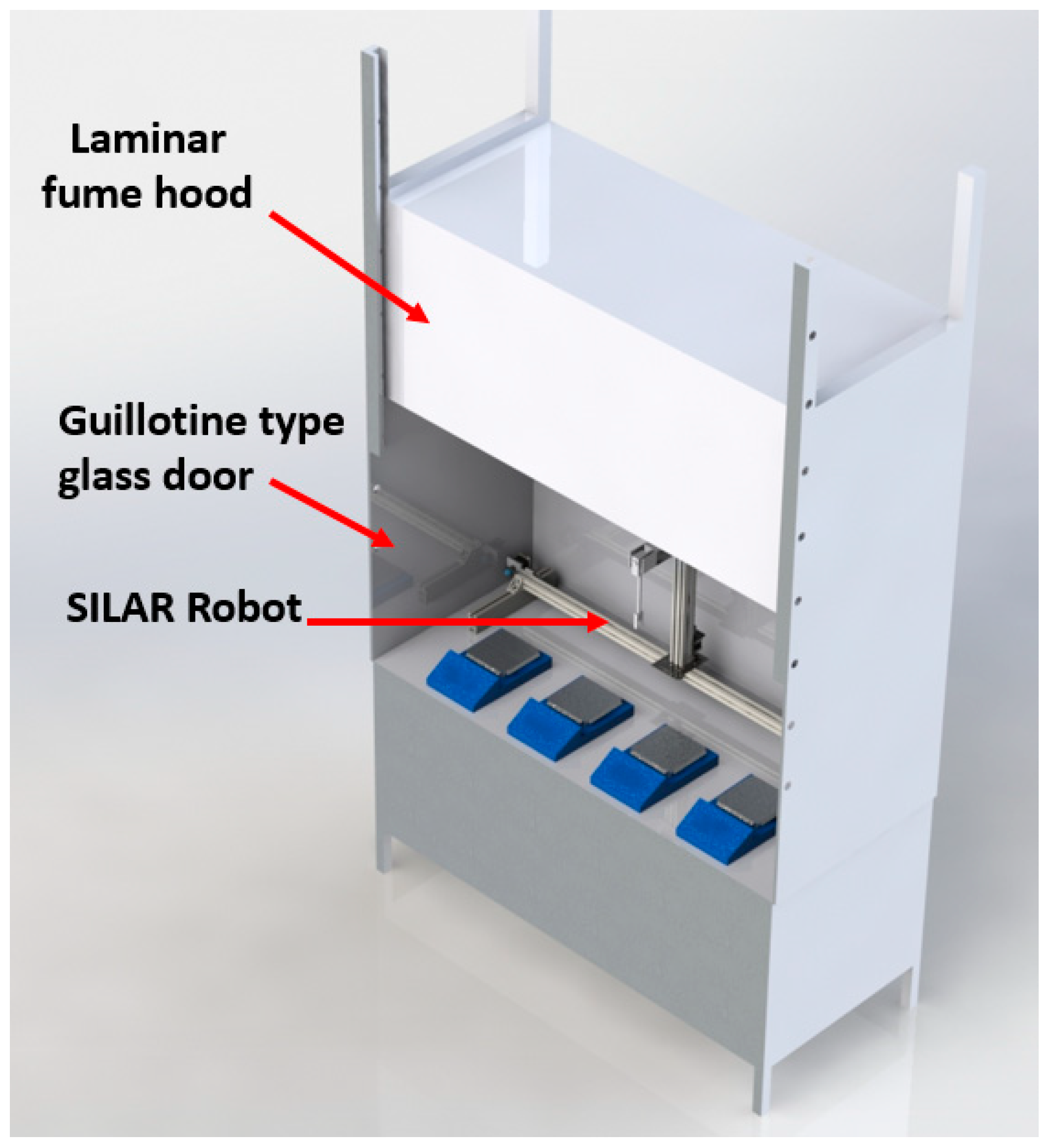
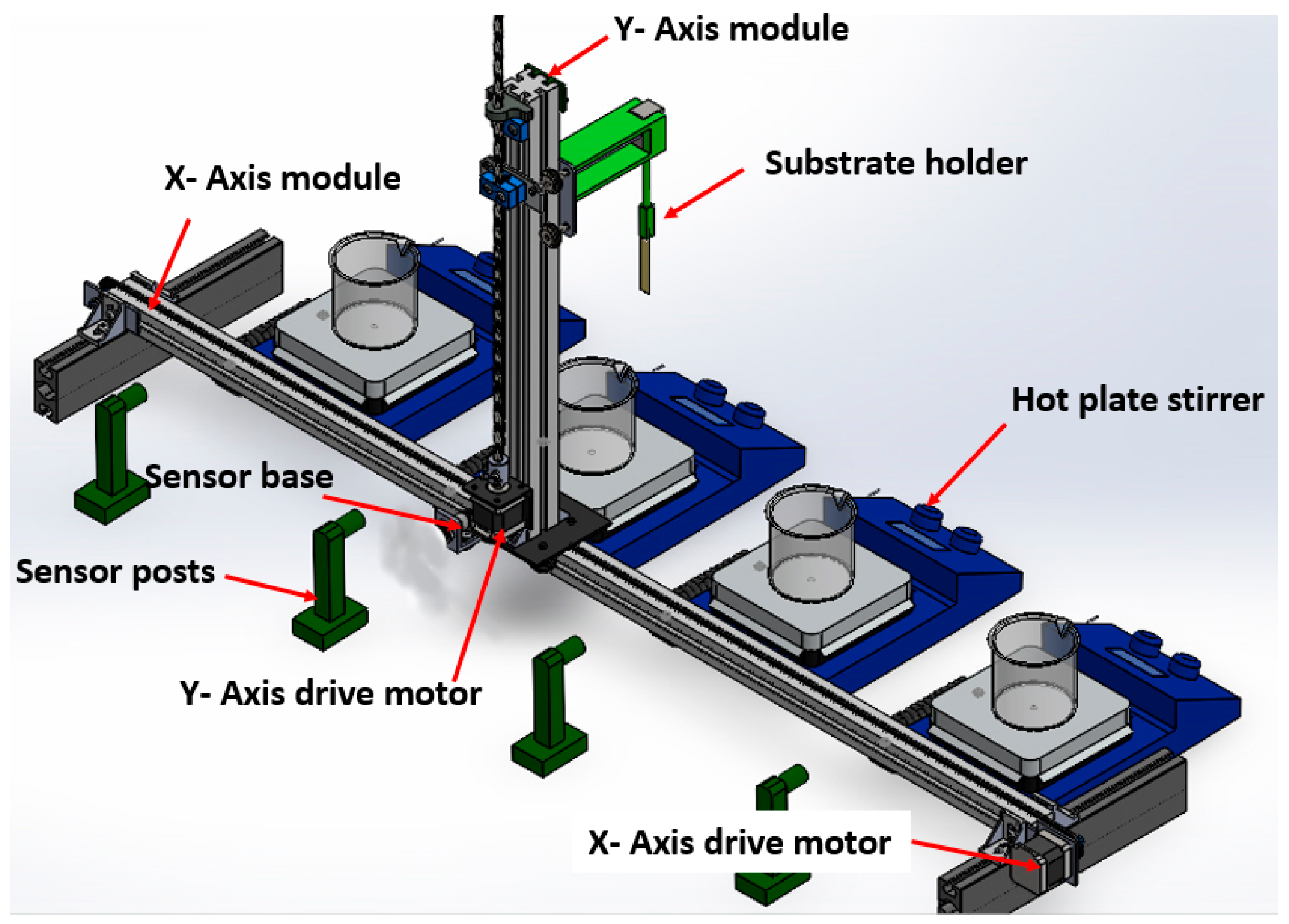
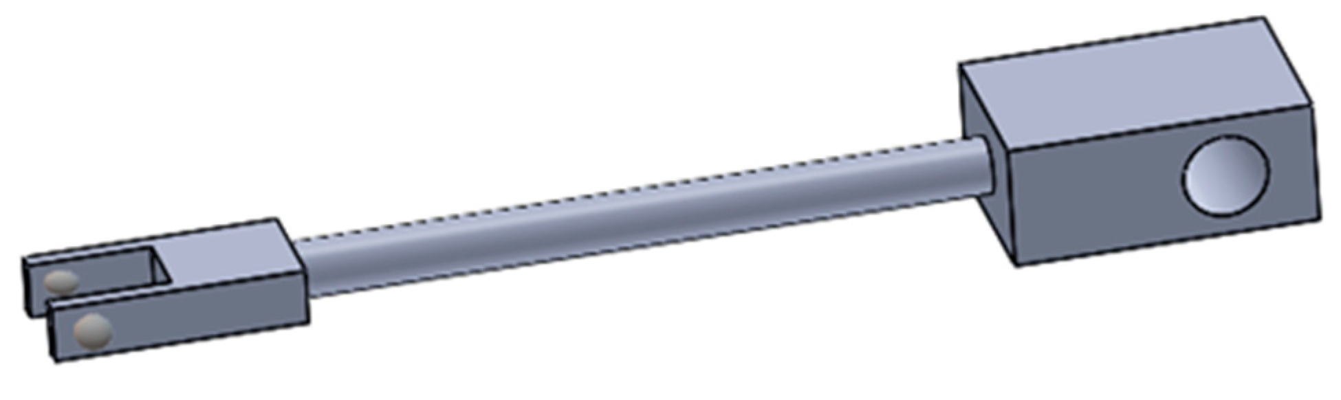
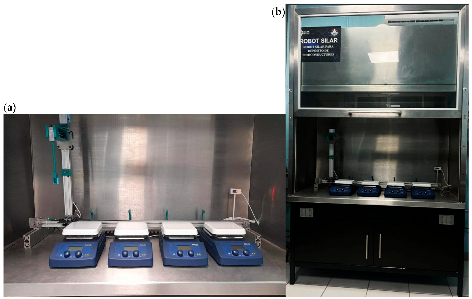
2.1. Design and Assembly of the Mechanical Elements
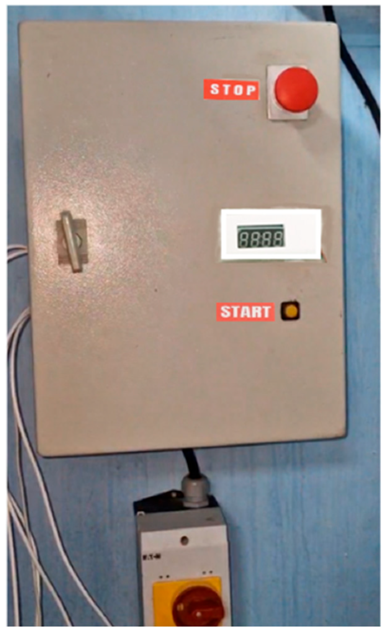
2.2. Electrical and Electronic Circuitry
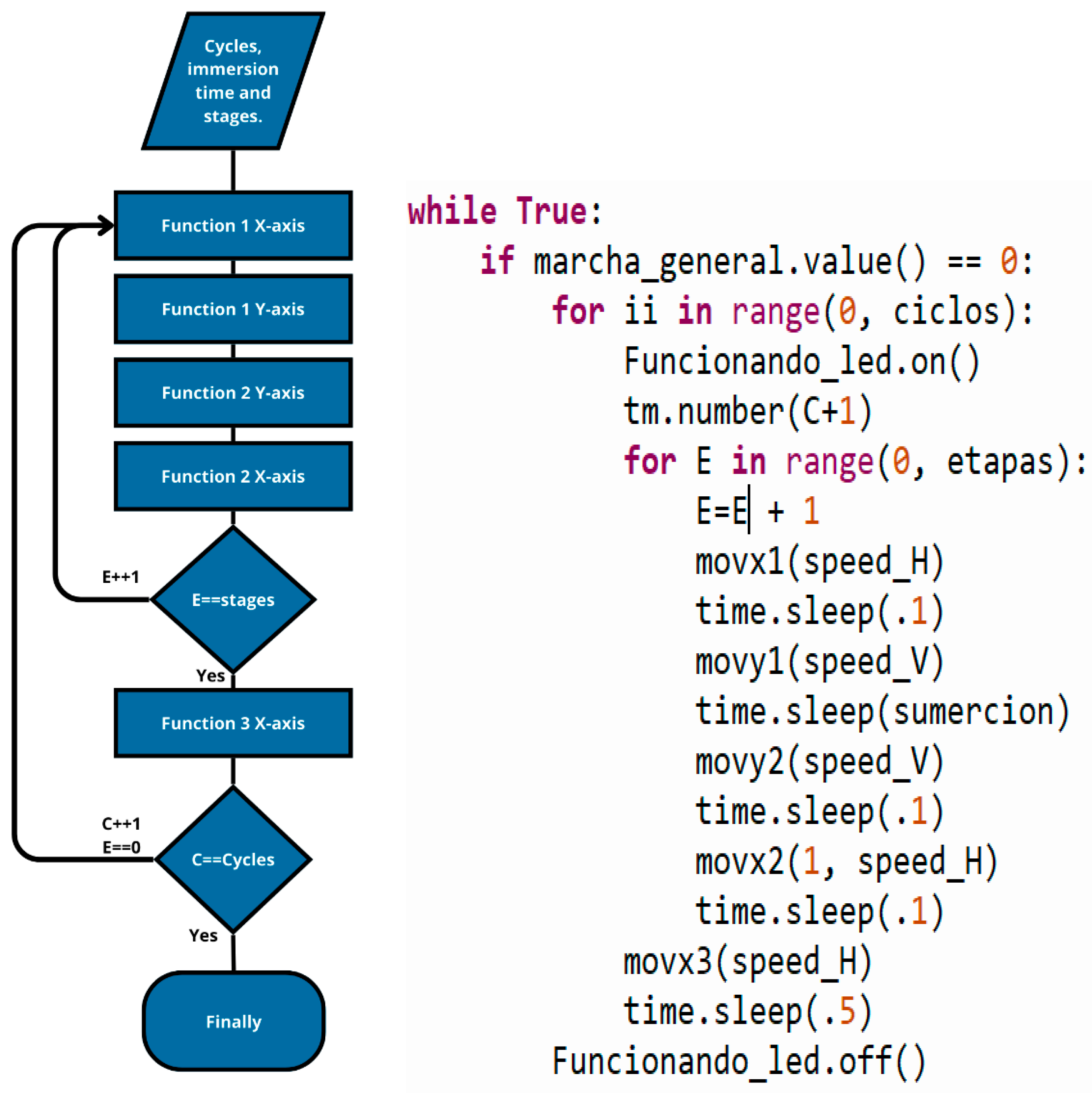
2.3. Automation and Communication Between the Interface and the System
- On the X-axis, three main functions are implemented:
- Function 1: Activates the X-axis motor to move the arm to the right until the follower sensor is triggered. Motor speed is precisely controlled using a PWM signal previously defined in the program.
- Function 2: Moves the arm slightly to deactivate the follower sensor, allowing Function 1 to be executed again. The motor is activated for 1 s and then automatically deactivated.
- Function 3: Moves the arm leftward to return it to the starting (home) position. The motor continues running until the X-axis micro switch is triggered, signaling the system to stop the movement.
- On the Y-axis, the following functions are implemented:
- Function 1: Activates the motor to move the arm downward for submersion. The motor continues running until the lower micro switch is triggered, at which point it stops automatically. Then a timer starts to record the submersion duration.
- Function 2: Activates the motor to move the arm upward, returning it to the initial position. The motor stops once the upper micro switch is triggered.
2.4. Deposition and Characterization of CZTS Thin Film
2.4.1. Substrate Cleaning
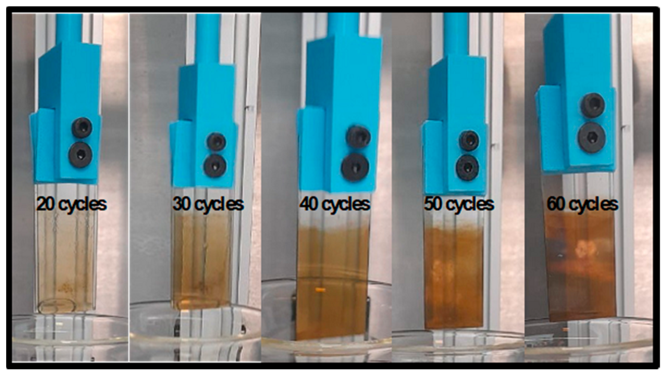
2.4.2. Deposition of CZTS Thin Film
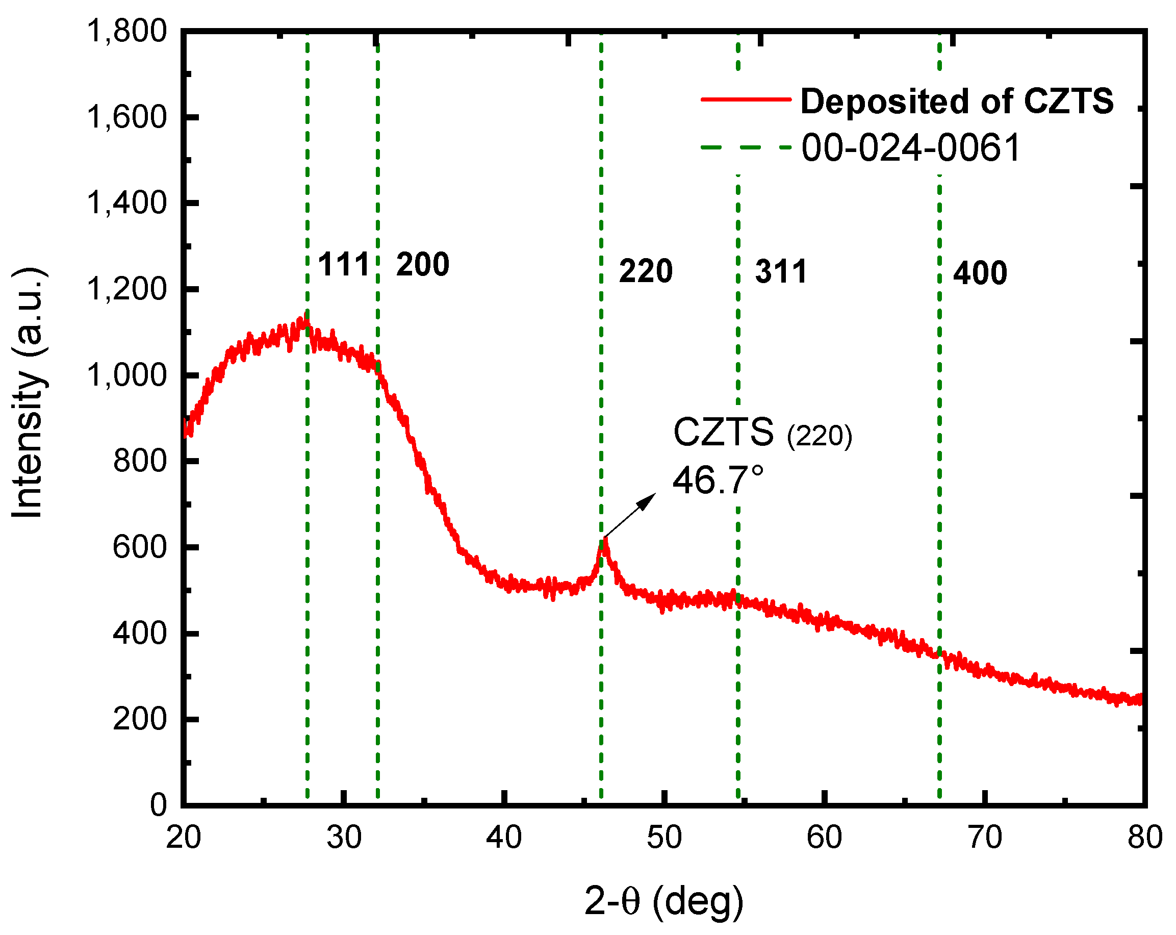
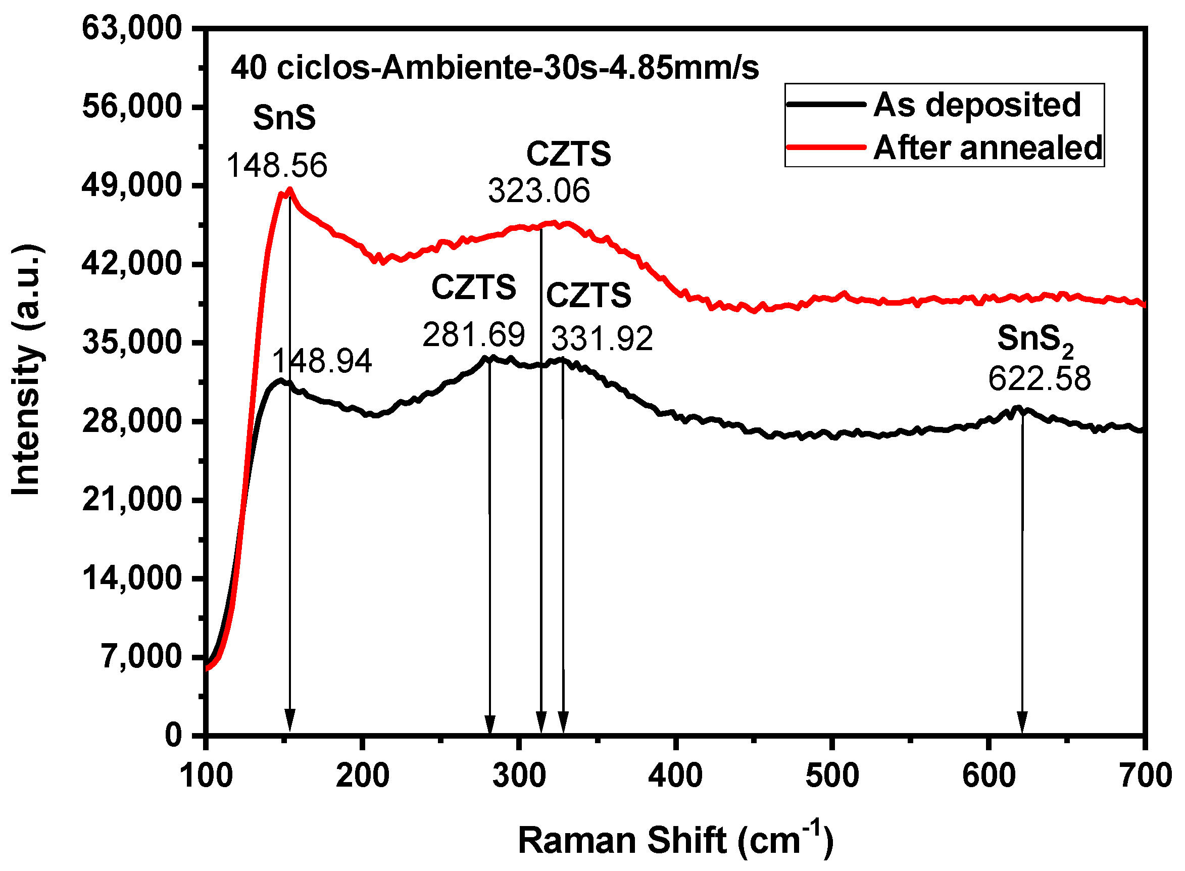
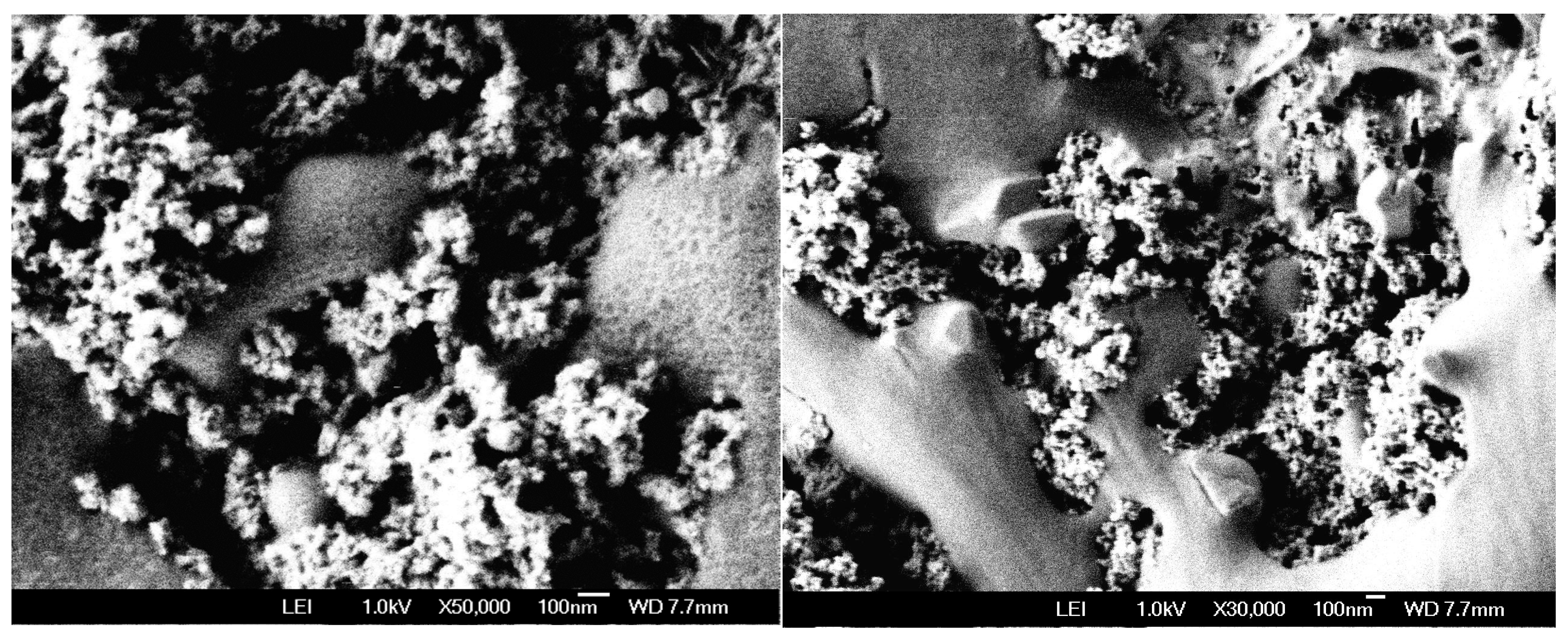
3. Results
4. Conclusions
Author Contributions
Funding
Institutional Review Board Statement
Informed Consent Statement
Data Availability Statement
Acknowledgments
Conflicts of Interest
References
- Capitaine, J.A.C. Automation of Carbon Nanostructure Synthesis by the Ultrasonic Spray Pyrolysis Method. Master’s Thesis, Monterrey Institute of Technology and Higher Education, Monterrey, Mexico, 2022. Available online: https://hdl.handle.net/11285/651117 (accessed on 20 June 2025).
- Muñoz, B.C.; Hernández Bedoya, S.F. Automation and Control of an Aerosol-Assisted Chemical Vapor Deposition (AACVD) System Using an Arduino Programming Board and Precision Sensors [Ponencia, Universidad Tecnológica de Pereira]. Universidad Tecnológica de Pereira. Available online: https://media.utp.edu.co/vicerrectoria-de-investigaciones/archivos/PONENCIA%20-%20ESTUDIO%20DE%20MATERIALES%20Y%20DESARROLLO%20DE%20TECNOLOGIAS%20PARA%20CALENTAMIENTO%20SOLAR.pdf (accessed on 20 June 2025).
- Reynoso, E.A.J.; Chávez-Cervantes, N.; Talamantes-Nieto, B. Automated fabrication of compact thin films in the development of Grätzel-type solar cells. J. Technol. Innov. 2017, 4, 36–42. [Google Scholar]
- Soonmin, H. Recent Advances in the Growth and Characterizations of SILAR-Deposited Thin Films. Appl. Sci. 2022, 12, 8184. [Google Scholar] [CrossRef]
- Gao, X.; Wang, X.Y. Synthesis and optical properties of ZnO nanocluster porous films deposited. Appl. Surf. Sci. 2004, 229, 275–281. [Google Scholar] [CrossRef]
- Altieri, W.M.; Sadafi, R.; Felix, S.; Boulfrad, S.; Lopes, R.; Prodanovic, S.; Kalantari, K.; Spanos, S.; Doeblinger, M.; Lichon, C.; et al. Development of an automated SILAR method for the sustainable fabrication of BiOI/TiO2 photoanodes. Energy Adv. 2024, 3, 2564–2574. [Google Scholar] [CrossRef] [PubMed]
- Valdez Martínez, J.; Martínez, M.A.; Camacho-Rangel, M.; Rodríguez, M.J.; Baca-Escobar, M.; Villarreal, T.J.; Baca-Escobar, B.E. Automation of the successive ionic layer adsorption and reaction (SILAR) process. Rev. Mex. Ing. Química 2020, 19, 1351–1361. [Google Scholar] [CrossRef]
- Azpeitia, H.J.; Martínez, M. Sistema de transporte para la deposición de películas de materiales iónicos por inmersión y método de operación. Jóvenes Investig. 2016, 1, 42–46. [Google Scholar]
- Suryawanshi, M.P.; Shin, S.W.; Ghorpade, U.V.; Gurav, K.V.; Hong, C.W.; Patil, P.S.; Moholkar, A.V.; Kim, J.H. Improved solar cell performance of Cu2ZnSnS4 (CZTS) thin films prepared by sulfurizing stacked precursor thin films via SILAR method. J. Alloys Compd. 2016, 671, 509–516. [Google Scholar] [CrossRef]
- Kaza, J.; Pasumarthi, M.R.; Avadhani, P.S. Superstrate and substrate thin film configuration of CdS/CZTS solar cell fabricated using SILAR method. Opt. Laser Technol. 2020, 131, 106413. [Google Scholar] [CrossRef]
- Kumar, K.G.; Bhargav, P.B.; Prakash, D.G.; Kaushik, R.; Mathew, E.R.; Shriram, M.K.; Veerathangam, K. Investigations on SILAR coated CZTS thin films for solar cells applications. Phase Transit. 2021, 94, 556–566. [Google Scholar] [CrossRef]
- Garzón Ramos, D.; Martínez, M.A.; Rodríguez, D.; Guzmán, G.D.; Castro, V. Sistema SILAR de producción para películas semiconductoras aplicadas en sensores de humedad. In Proceedings of the 16 Convención Científica de Ingeniería y Arquitectura, Havana, Cuba, 26–30 November 2012. [Google Scholar]
- Sen Gupta, A.K.; Adnan, A.; Bhattacharjee, S.; Das, N.K.; Matin, M.A.; Quamruzzaman, M. SnapFib: An Easy Build Arduino-based Tabletop Prototype for Thin Film Deposition by Successive Ionic Layer Adsorption and Reaction Method. Mendeley Data, V4. 2022. Available online: https://data.mendeley.com/datasets/3pccd4yp8m/4 (accessed on 20 June 2025).
- Júnior, S.L.; Segundo, I.R.; Freitas, E.; Vasilevskiy, M.; Carneiro, J.O.; Tavares, C.J.M. Use and misuse of the Kubelka-Munk function to obtain the band gap energy from diffuse reflectance measurements. Solid State Commun. 2022, 341, 114573. [Google Scholar]
- Chamekh, S.; Khemiri, N.; Kanzari, M. Effect of annealing under different atmospheres of CZTS thin films as absorber layer for solar cell application. SN Appl. Sci. 2020, 2, 1507. [Google Scholar] [CrossRef]
- Touati, R.; Rabeh, M.B.; Kanzari, M. Effect of post-sulfurization on the structural and optical properties of Cu2ZnSnS4 thin films deposited by vacuum evaporation method. Thin Solid Film. 2015, 582, 198–202. [Google Scholar] [CrossRef]
- Lakhe, M.G.; Bhand, G.; Rohom, A.; Londhe, P. Electrochemical Synthesis and Characterization of Cu2ZnSnS4 Thin Films. J. Mater. Sci. Eng. 2016, 5, 1000261. [Google Scholar] [CrossRef]
- Suryawanshi, M.P.; Shin, S.W.; Ghorpade, U.V.; Gurav, K.V.; Hong, C.W.; Agawane, G.L.; Vanalakar, S.A.; Moon, J.H.; Yun, J.H.; Patil, P.S.; et al. Moholkar, Improved photoelectrochemical performance of Cu2ZnSnS4 (CZTS) thin films prepared using modified successive ionic layer adsorption and reaction (SILAR) sequence. Electrochim. Acta 2014, 150, 136–145. [Google Scholar] [CrossRef]
- Buldu, D.G.; Cantaş, A.; Turkoglu, F.; Akca, F.; Meriç, E.; Özdemir, K.M.; Tarhan, E.; Ozyuzer, L.; Aygun, G. Influence of sulfurization temperature on Cu2ZnSnS4 absorber layer on flexible titanium substrates for thin film solar cells. Phys. Scr. 2018, 93, 024002. [Google Scholar] [CrossRef]
- Zhang, X.; Fu, E.; Zheng, M.; Wang, Y. Fabrication of Cu2ZnSnS4 Thin Films from Ball-Milled Nanoparticle inks under Various Annealing Temperatures. Nanomaterials 2019, 9, 1615. [Google Scholar] [CrossRef] [PubMed]
- Chaudhari, J.J.; Joshi, U.S. Optimization of Cu2ZnSnS4 thin film absorber layer growth without sulphurization using triethanolamine as complexing agent for thin film solar cells applications. J. Mater. Sci. Mater. Electron. 2018, 29, 7048–7056. [Google Scholar] [CrossRef]
- Vázquez-González, P.J.; Paniagua-Chávez, M.L.; Zebadua-Chavarria, L.A.; Mota-Grajales, R.; Meza-Avendaño, C.A.; Campos-González, E.; Escobosa-Echavarría, A.; Hu, Y.; Pérez-Ramos, A.E.; Manuel-Matuz; et al. Comprehensive Structural, Chemical, and Optical Characterization of Cu2ZnSnS4 Films on Kapton Using the Automated Successive Ionic Layer Adsorption and Reaction Method. Nanomaterials 2025, 15, 85. [Google Scholar] [CrossRef] [PubMed]


| Parameter | |||||
|---|---|---|---|---|---|
| Number of cycles | 20 | 30 | 40 | 50 | 60 |
| Immersion time of the solution | 30 s | 30 s | 30 s | 30 s | 30 s |
| Immersion of rinsing time | 30 s | 30 s | 30 s | 30 s | 30 s |
| Precursor temperature | Room | Room | Room | Room | Room |
| Rinse temperature | Room | Room | Room | Room | Room |
| Dip speed | 31.8 m/s | 31.8 m/s | 31.8 m/s | 31.8 m/s | 31.8 m/s |
| Deposited Time | 48 m | 72 m | 96 m | 120 m | 144 m |
| Cycles | Thickness |
|---|---|
| 40 | 1.49 µm |
| 50 | 1.54 µm |
| 60 | 1.61 µm |
Disclaimer/Publisher’s Note: The statements, opinions and data contained in all publications are solely those of the individual author(s) and contributor(s) and not of MDPI and/or the editor(s). MDPI and/or the editor(s) disclaim responsibility for any injury to people or property resulting from any ideas, methods, instructions or products referred to in the content. |
© 2025 by the authors. Licensee MDPI, Basel, Switzerland. This article is an open access article distributed under the terms and conditions of the Creative Commons Attribution (CC BY) license (https://creativecommons.org/licenses/by/4.0/).
Share and Cite
Vázquez-González, P.J.; Paniagua-Chávez, M.L.; Mota-Grajales, R.; Hernández-Gutiérrez, C.A. Automated SILAR System for High-Precision Deposition of CZTS Semiconductor Thin Films. Micro 2025, 5, 32. https://doi.org/10.3390/micro5030032
Vázquez-González PJ, Paniagua-Chávez ML, Mota-Grajales R, Hernández-Gutiérrez CA. Automated SILAR System for High-Precision Deposition of CZTS Semiconductor Thin Films. Micro. 2025; 5(3):32. https://doi.org/10.3390/micro5030032
Chicago/Turabian StyleVázquez-González, Perla J., Martha L. Paniagua-Chávez, Rafael Mota-Grajales, and Carlos A. Hernández-Gutiérrez. 2025. "Automated SILAR System for High-Precision Deposition of CZTS Semiconductor Thin Films" Micro 5, no. 3: 32. https://doi.org/10.3390/micro5030032
APA StyleVázquez-González, P. J., Paniagua-Chávez, M. L., Mota-Grajales, R., & Hernández-Gutiérrez, C. A. (2025). Automated SILAR System for High-Precision Deposition of CZTS Semiconductor Thin Films. Micro, 5(3), 32. https://doi.org/10.3390/micro5030032